Lecturer
|

|
Memory Products 64M..2G Bit DRAM

|

|
- Memory test and fault diagnosis for yield enhancement
- Reliability studies for product qualification
- Verification of digital and analog circuits
Important Events

|
18.-21.11.2025 PRODUCTRONICA weltleitmesse für innovative elektronikfertigung, München |

|
electronica 10.-13.11.2026 components / systems / applications München |

|
embedded world Conference 10.-12.3.2026, Nürnberg, Germany |

|
Allgäuer Hochschulmesse, 2026, Kempten |
References
|
CMOS: Circuit Design, Layout, and Simulation, Revised Second Edition, R. Jacob Baker, Wiley, ISBN 978-0-470-22941-5, Revised 2nd Edition, 2008. CMOS: Mixed-Signal Circuit Design, Second Edition, Baker, Wiley 2009 CMOSedu.com Data Conversion Handbook (Analog Devices) Walter Kester 64 Euro Data Conversion Handbook pdf Analog Dialogue University Program Online Teaching Material |

|
References
|
EE247 Analog-Digital Interface Integrated Circuits Instructor: Haideh Khorramabadi http://inst.eecs.berkeley.edu/~ee247/fa09/index.html on Wayback machine archive.org Murmann, Stanford EE315B - VLSI Data Conversion Circuits https://www.stanford.edu/group/murmann_group/cgi-bin/mediawiki/index.php/Boris_Murmann |
|
Course Description EE247
Architectural and circuit level design and analysis of integrated analog-to-digital and digital-to-analog interfaces in modern CMOS and BiCMOS VLSI technology.
Analog-digital converters: Nyquist and over-sampled, digital-analog converters, sample/hold amplifiers, continuous-time and switched-capacitor filters.
Low power mixed signal design techniques.
Data communication systems including interface circuitry.
CAD tools for analog design for simulation and synthesis.
References
|
CMOS Analog Circuit Design Philip Allen, Douglas Holberg http://www.aicdesign.org/ https://aicdesign.org/2016-short-course-notes-2/ 2nd Edition of the book has data converters. Some editions don't have data converters. |
|
Analog Digital Interface Circuits
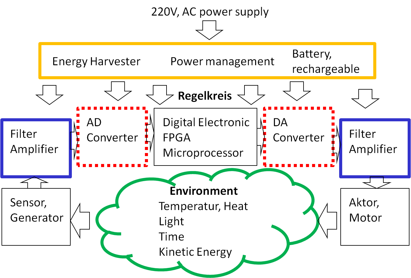
- Naturally occuring signals are analog
- Why are data converters and digital signal processing used?
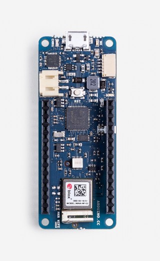
Example Arduino MKR WIFI 1010
Analog Calibration
|
|
Arduino ADC, DAC project
Minimum value of ADC: 0
Maximum value of ADC 1021
Minimum voltage: 30 mV
Maximum voltage: 3.31 V
Sampling rate: 289.28 Hz
Minimum value of ADC: 0
Maximum value of ADC 1021
Minimum voltage: 30 mV
Maximum voltage: 3.31 V
Sampling rate: 289.28 Hz
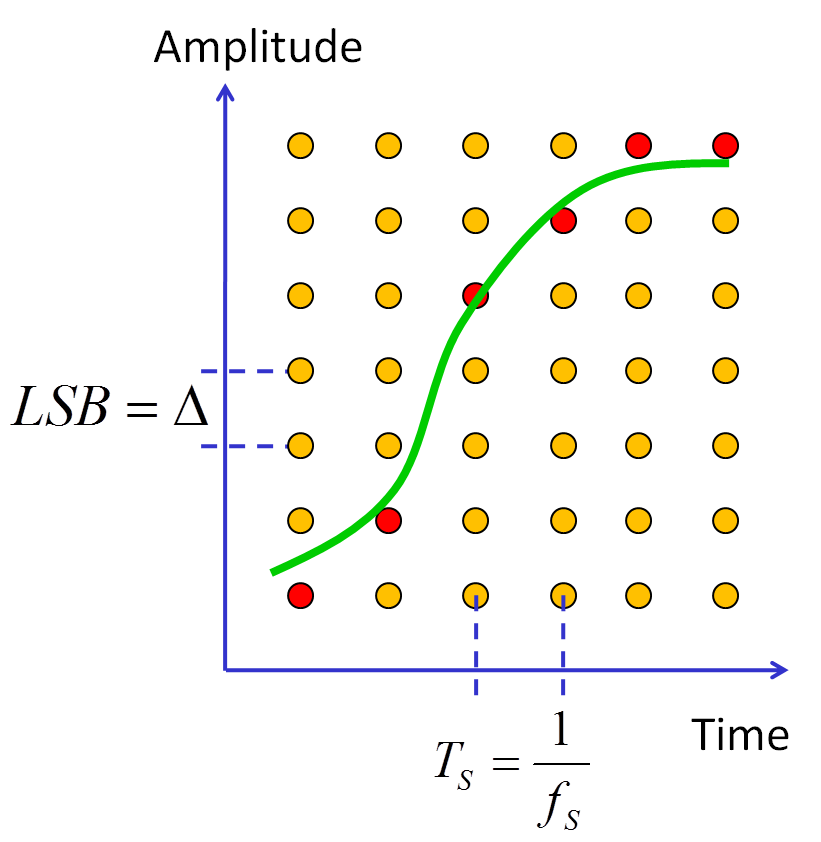
Properties of digital signals
Properties:
|
|
The green analog curve is discretized in time and level resulting in the red points.
The smallest difference in level is called delta Δ or LSB (least significant bit).
The smallest difference in time is called sampling time (ts).
The smallest difference in level is called delta Δ or LSB (least significant bit).
The smallest difference in time is called sampling time (ts).
Data converter application: software defined radio SDR

A tuneable filter provides a limited bandwidth to an ADC.
The radio protocol (WiFi, Bluetooth, FM, AM, digital-TV,LTE)
is realized in the digital signal processing block.
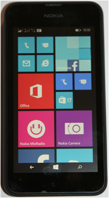
Data converter application: Mobile phone
|
Filters Number of data converters: HSDP, LTE, UMTS, WLAN, bluetooth motion, pressure, proximity sensor speaker, microphone display control |
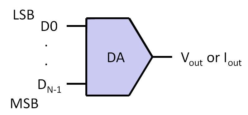
Digital to analog converter metric
|
 \[ \Delta = \frac{V_{ref}}{2^N} \]
\[ N = log_2 \frac{V_{ref}}{\Delta} = ld \frac{V_{ref}}{\Delta} \]
\[ V_{max} = V_{ref}- \Delta \]
\[ \Delta = \frac{V_{ref}}{2^N} \]
\[ N = log_2 \frac{V_{ref}}{\Delta} = ld \frac{V_{ref}}{\Delta} \]
\[ V_{max} = V_{ref}- \Delta \]
|
\[ V_O = V_{ref} \sum_{i=0}^{N-1} \frac{D_{i}}{2^{N-i}} \] \[ V_O = \Delta \sum_{i=0}^{N-1} D_{i} \cdot 2^{i} \]
Attention: Vref, Vmax, VFS
Analog devices Data Converter book sometimes states VFS = Vref
Baker (Equation 28.8) and Texas Instruments Understanding Data converters define VFSR = Vmax
In some circuit architectures Vref = Vmax
Watch out and act accordingly.