Interface Electronics
Laboratory 03: ADC DAC Analysis
Lab03 GroupA, ***910 A, ***726 P
|
|
Laboratory Goals
The objectives of this laboratory session are as follows:
- Simulation of an ideal ADC connnected to a DAC.
- Data analysis of the output of the ideal ADC DAC with ramp signal as an input including DNL, INL and LSB.
- Data analysis of the output of the ideal ADC DAC with sine signal as an input including DNL, INL, FFT data processing and SNR.
- Simulation a data converter with a real 4-bits R2R DAC.
- Data analysis of the data converter with a real 4-bits R2R DAC with ramp signal as an input including DNL, INL and LSB.
- Data analysis of the data converter with a real 4-bits R2R DAC with sine signal as an input including FFT data processing DNL, INL and SNR.
- LTspice data extraction.
Simulation and Analysis of 4-bits ADC DAC With Ramp Input Signal
The following ideal 4-bits ADC DAC was simulated in LTspice:
Simulation and Analysis of 4-bits ADC DAC With Ramp Input Signal
| The following figure shows the simulated citcuit: |
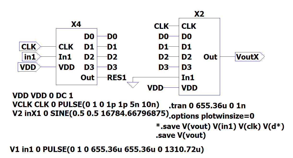 figure 1
|
Simulation and Alaysis of 4-bits ADC DAC With Ramp Input Signal
| The following figure was obtained from the simulation. It shows the ramp input signal to the ADC and the digitalized output from the DAC. |
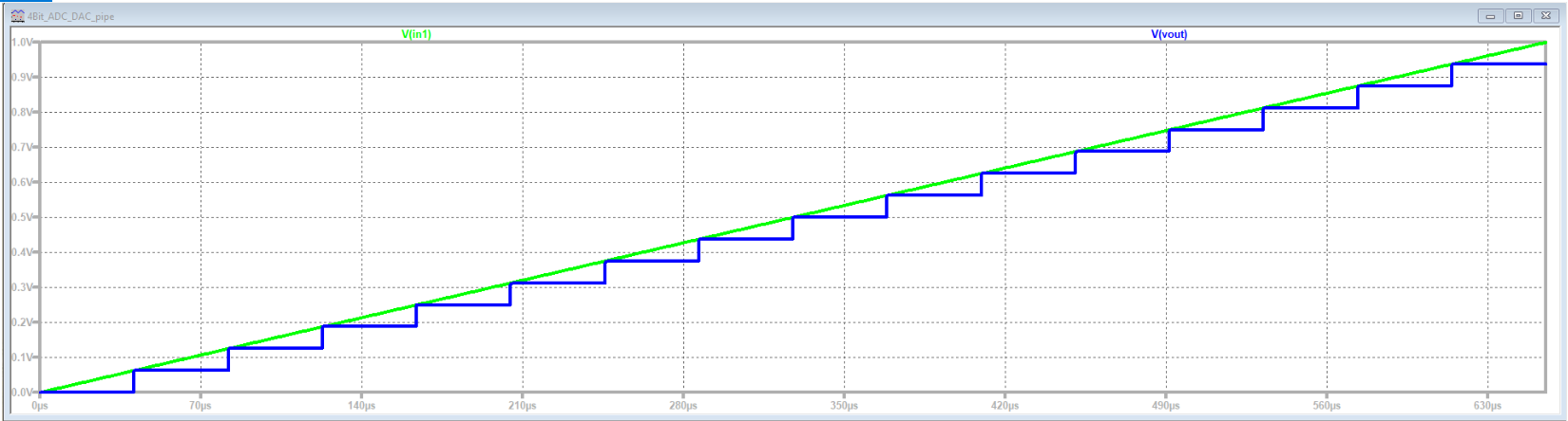 figure 2
|
Simulation and Analysis of 4-bits ADC DAC With Ramp Input Signal
- Since LTspice provides huge amount of simulated data which might contains some distubances, there was a need to analyse the simulated values using
some other ways.
- Luckly,the LTspice generates a raw file with the simulated values, these values can be read, extracted, filtered and analysed using a provided
JavaScrip tool (Read Raw File). This tool allows us to read the LTspise raw file and apply a filter to the data with previously specified time steps.
- The start time for the analysis was zero, the stop time was 655.36us which is the stop time of the simulation and the time step was 40.96us,
this time step was calculated by dividing the total time by the number of steps obtained from the simulation. The LTspice raw file should be uploaded to JavaScript tool and specifiying the time.
Simulation and Alaysis of 4-bit ADC DAC With Ramp Input Signal
| The following two figures show the data analysis of the ramp input singal. The upper figure shows the ideal and the extracted output of the ADC DAC . As the data converter is ideal, it is obvious that the extracted output is identical to the ideal one. While the lower curve shows the INL and DNL errors. As it is also clear that there is no errors since the data converter is ideal. |
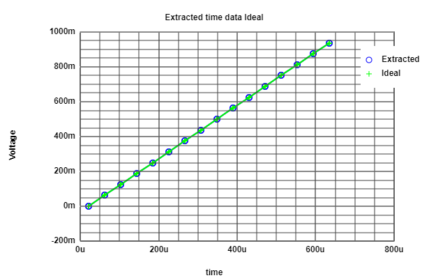 figure 3
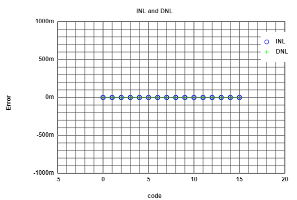 figure 4
|
Simulation and Alaysis of 4-bits ADC DAC With Ramp Input Signal
- A histogram curve was also obtained from the analysed data. For the Historgam, more time step was needed, so that the time step was changed in the JavaScript tool to 512us. The upper firue shows the obtained Historgam curve.
- Since this curve is obtained from ideal ADC DAC data converter, it is an ideal curve, so that diffirent time steps cannot be seen. While the lower curve to the right hand shows the Historam with the extracted data, as it is obvious that some errors are presented since the histogram curve in this case is not useful.
|
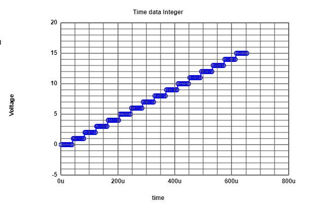 figure 5
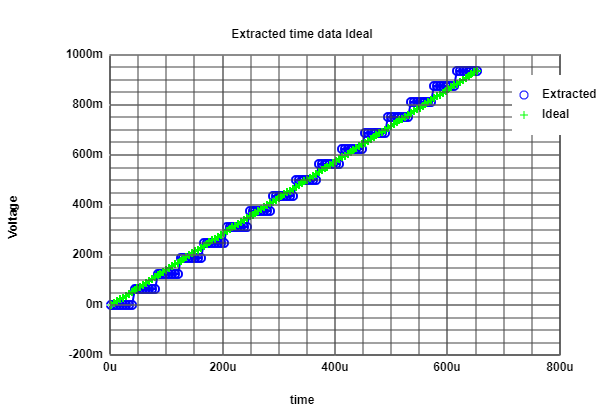 figure 6
|
Simulation and Alaysis of 4-bit ADC DAC with Sine Input Signal
- The same previously mentioned 4-bits ADC DAC but with sine input signal was also simulated and analysed using the provided JavaScript tool.
- The following two figures were obtained from the simulation. The upper curve shows the sine input to the ADC and the digitalized outpu. While lower curve shows the FFT analysis obtained from LTspice.
|
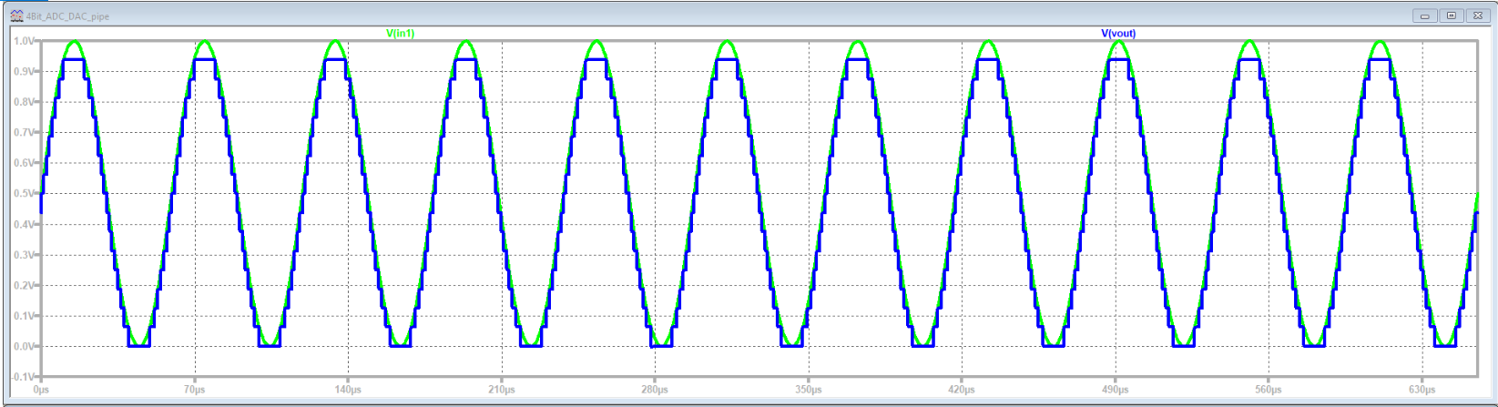 figure 7
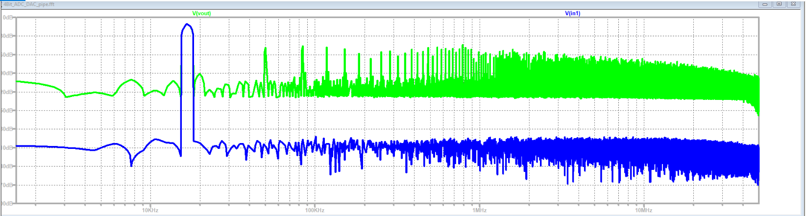 figure 8
|
Simulation and Alaysis of 4-bits ADC DAC with Sine Input Signal
| The follwing two figures where obtained from the JavaScript tool after analysing the LTspice raw file. From the upper figure shows the extracted data of the sine input. While the lower figure shows the typical curve of the sine function of the DNL and the INL. |
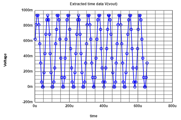 figure 9
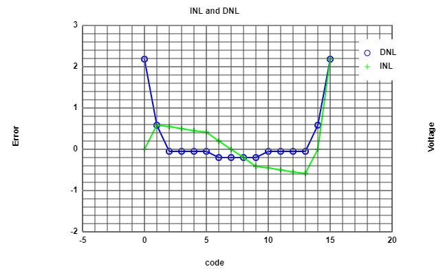 figure 10
|
Simulation and Alaysis of 4-bits ADC DAC with Sine Input Signal
After analysing the extracted data from LTspice using the provided JavaScript tool, another JavaScript tool was also provided to do the FFT anaysis. The following figures were obtained from the FFT analysis
the left hand side figure shows the analysis results with 10-bits, while the right hand side figure shows the anaylsis with 4-bits.
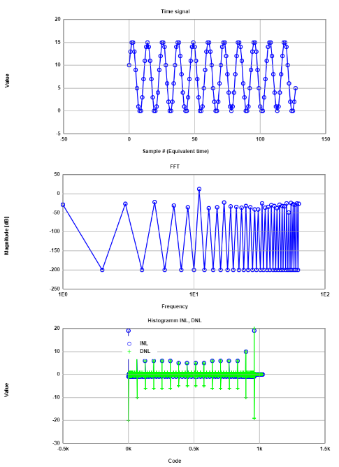 figure 11
|
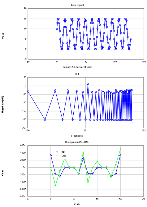 figure 12
|
From the previous figures of DNL and INL, we can see that the figure to the left hand side does not present real DNL and INL values, while the figure to the right hand side shows the real values since the number of bits of this data converter is 4-bits.
Simulation and Alaysis of 4-bit ADC DAC with Sine Input Signal (Singal to Noise Ratio)
| In the following table shows the SNR which was obtained from the FFT analysis: |
| Frequency (Hz) |
Sinal magnitude (dB) |
Total signal noise (dB) |
| 11 |
11.87 |
-13.89 |
| 5 |
-21.56 |
-14.7 |
| 17 |
-23.64 |
-15.3 |
| 55 |
-24.16 |
-15.9 |
| 61 |
-25 |
-16.47 |
| 51 |
-25.62 |
-17.04 |
| 33 |
-25.67 |
-17.68 |
| 63 |
-26.33 |
-18.31 |
| 3 |
-6.86 |
-18.96 |
| 57 |
-27.66 |
-19.59 |
| 1 |
-28.4 |
-20.21 |
| From this table, the number of bits can be calculated by subtracting the total signal noise from the singal noise and then dividing the result by 6, the result is 4 bits. |
Simulation and Alaysis of a Data Converter with a Real DAC
A ADC with a real R2R DAC was simulated. Two circuits were simulated. One with right DAC resistor values (the circuit to the left hand side), and another DAC with filled errors (the circuit to the right hand side) where the values of R6 and R10 were changed; R6 was changed from 1 Ohm to 1.3 Ohm, and R9 was changed from 2 Ohm to 1.5 Ohm
Simulation and Alaysis of a Data Converter with a Real DAC
| The following figure shows the simulated data converter with real R2R DAC and correct resistos values. |
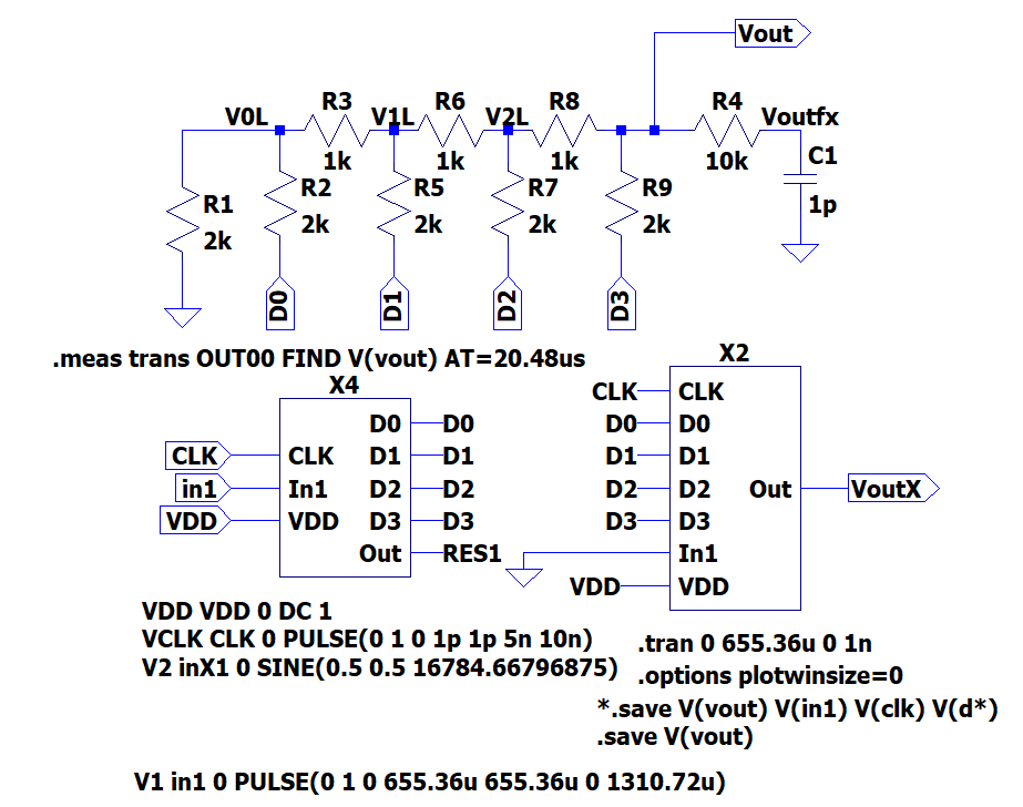 figure 13
|
Simulation and Alaysis of a Data Converter with a Real DAC
| The following figure shows the simulated data converter with real R2R DAC and correct resistos values. |
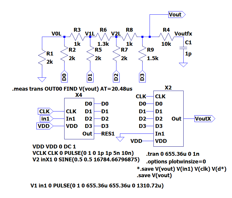 figure 14
|
Simulation and Alaysis of a Data Coverter With a Real DAC With Ramp Input Signal
| The following figures were obtained from the simulation of a ramp input signal. The upper figure shows the output ramp signal of the data converter without filling errors, while the lower figure shows some errors: |
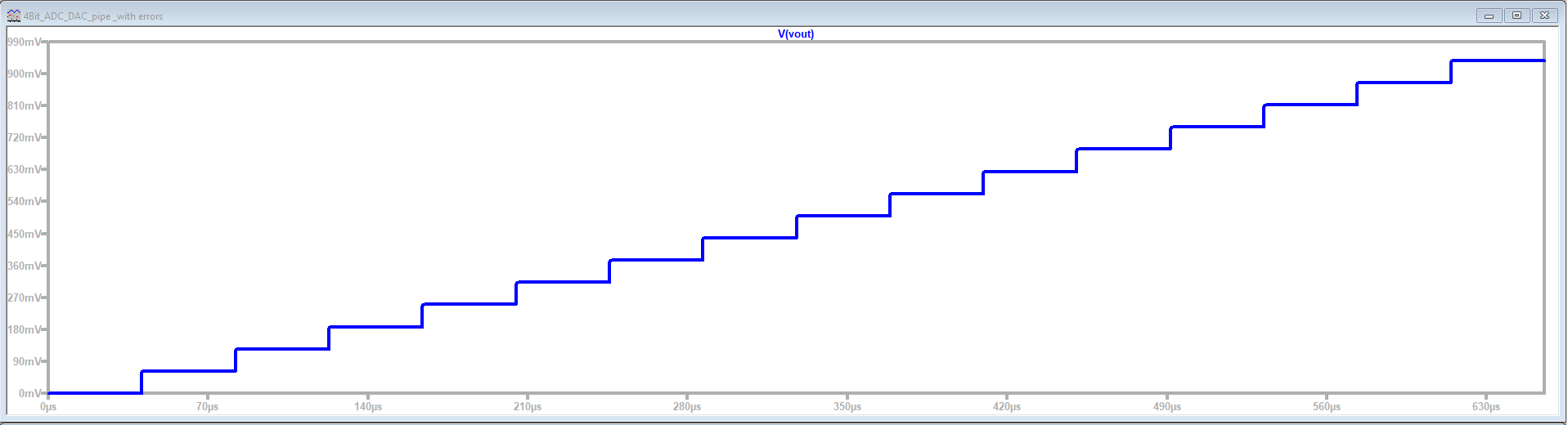 figure 15
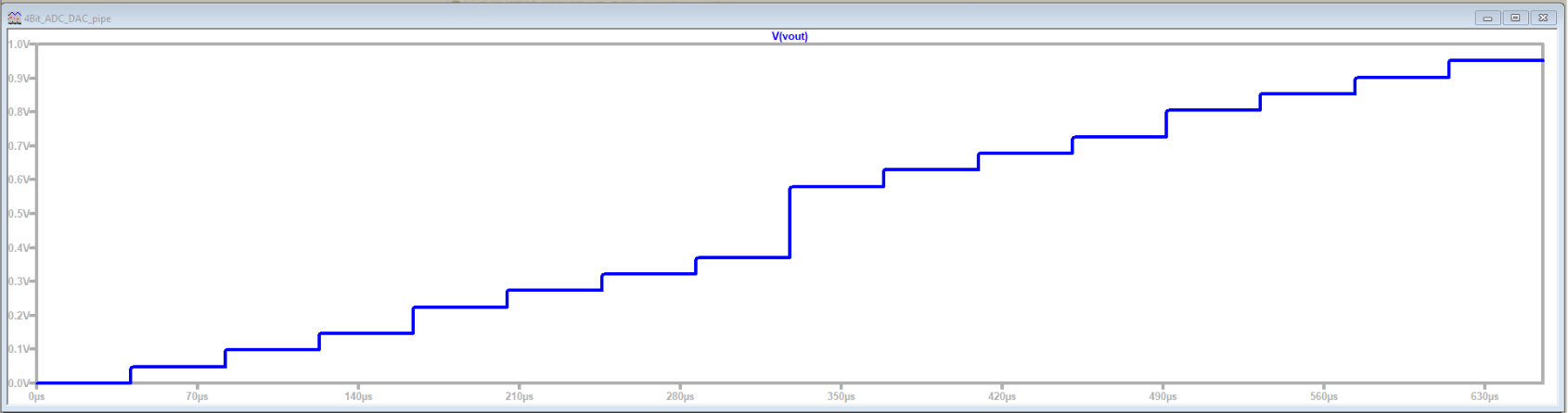 figure 16
|
Simulation and Alaysis of a Data Coverter With a Real DAC With a Sine Input Signal
| The following curves were obtained from the simulation of a sine input signal. The upper figure shows the output sine signal of the data converter
without filling errors, while the lower figure shows some errors presented as big jumps in the center of the waveform. |
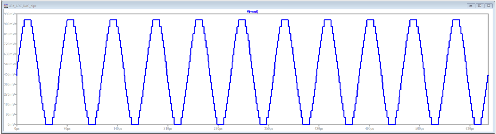 figure 17
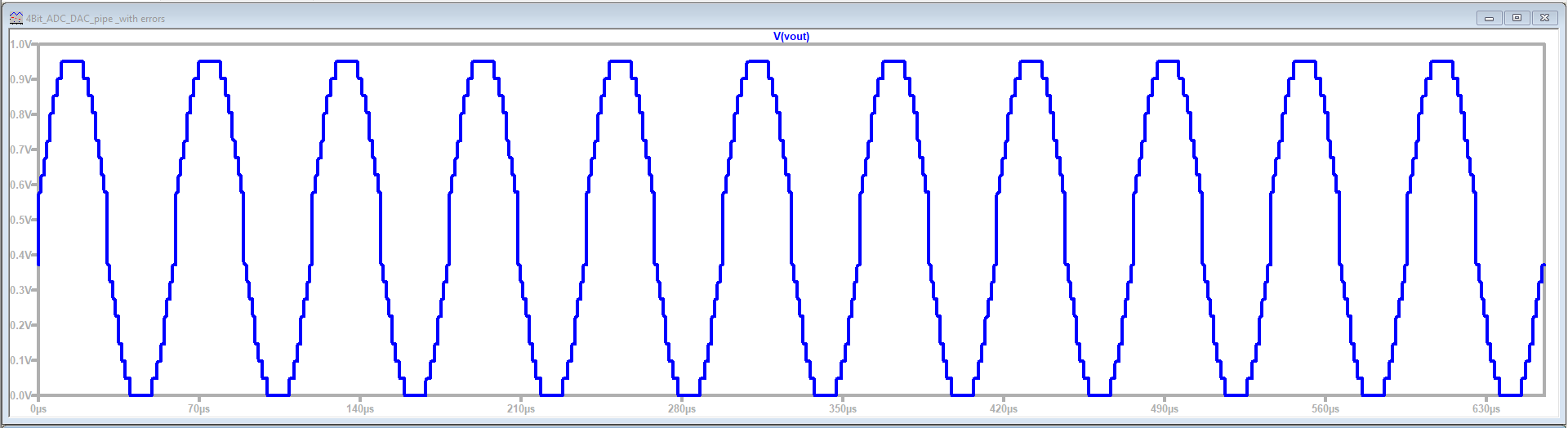 figure 18
|
Simulation and Alaysis of a Data Coverter With a Real DAC With a Sine Input Signal
| The following curves were obtained from the FFT analysis of the simulated values with filling errors. |
figure 19
|
The above DNL INL figure shows that some values are bigger than one and smaller that -1 indicating the errors in the simulated values.
Simulation and Analysis of a Data Coverter With a Real DAC With a Sine Input Signal (Signal to Noise Ratio)
The following table, SNR were obtained from the FFT analysis:
| Frequency (Hz) |
Sinal magnitude (dB) |
Total signal noise (dB) |
| 11 |
12.09 |
-6.75 |
| 33 |
-11.33 |
-8.6 |
| 3 |
-16.04 |
-9.47 |
| 7 |
-16.71 |
-10.37 |
| 51 |
-16.76 |
-11.51 |
| 55 |
-18.18 |
-12.56 |
| 15 |
-20.43 |
-13.33 |
| 5 |
-20.86 |
-14.18 |
| 29 |
-22.75 |
-14.83 |
| 317 |
-22.76 |
-15.59 |
| 9 |
-23.53 |
-16.35 |
From this table, the number of bits can be calculated, subtracting the total signal noise from the singal noise and then dividing the result by 6, the result is 3 bits which means that one bit is missing due to the occured errors.
LTspice Log Error
| The following curve was obtained from the simulation of the ramp input signal. It shows the LTspice Error Log for a specified time.
This time can be speficied by the user. The command (.meas) was used. |
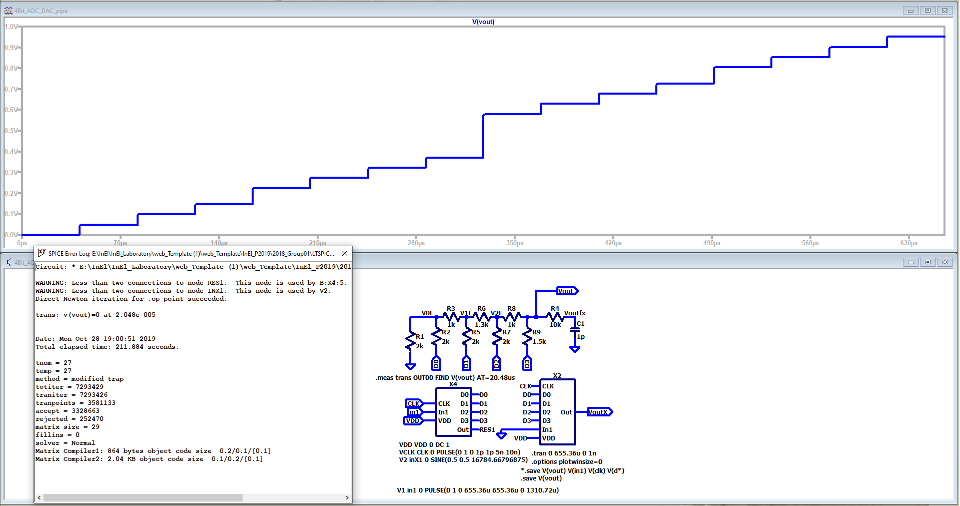 figure 20
|
Challenges and Difficulties
While implementing this laboratory session, some challenges and difficulties were faced. These challenges and difficulties are listed below:
- The simulation was a bit slow, which needed some time.
- The analysis needed some time to read, extract and filter the data after providing the raw file
- The FFT analysis of the simulated data was not understandable. The reason might be the lake of knowledge in analysing the FFT analysis.
- A lot of time was spent on editing the webpage raw code. Since some points were not clear enough and some research was needed to be able to complete the report.
But dispite of this, there was still a problem inserting an LTspice schematics.
The main two challenges of this laboratory session were the time needed and the lake of knowldge analysing the simulated data and editing the webpage code.
Leassons Learned and Time Spent
The following lessons were learned out of this laboratory session:
- Simulation using LTspice.
- Data extraction from LTspice.
- Data analysis using the JavaScript tool.
- DNL, INL and LSB calcuations.
- Edition of the raw html code for the webpage.
The time spent working on this laboratory was around 25 hours distributed between the lab session, implemnting the simulations, analysing the data and working on the report.
Most of the time was spent of editing the code of the web page
Conclusion
From this laboratory session, we conclude the following:
- During this lab, an ideal ADC DAC was simulated with given data steps The simulated data was read, extracted, filtered and analysed using a provided JavaScript tool (Read Raw File).
- A data converter with a real R2R DAC was also simulated with given data steps. Also, the simulated data was read, extracted, filtered and analysed.
- Two input signals were applied to the ideal ADC DAC as well as to the data converter with the R2R DAC including a sine and a ramp waveforms.
- Correct values of resistors in the real R2R DAC were simulated. In addition to wrong values for the comparative purpuses.
- Calculating DNL and INL was done during the analysis. In addition to FFT analysis
- Using a html webpage to publish the laboratory´s report was successfully achieved.
- Extracting data from LTspice using (Excute .meas script) prodived from LTspice tools was also done.
Clarification
The work on this lab session including the simulation implementation and work on the report was done in group.
The simulation was done in cooperation between the two group members as well as the web report creation.