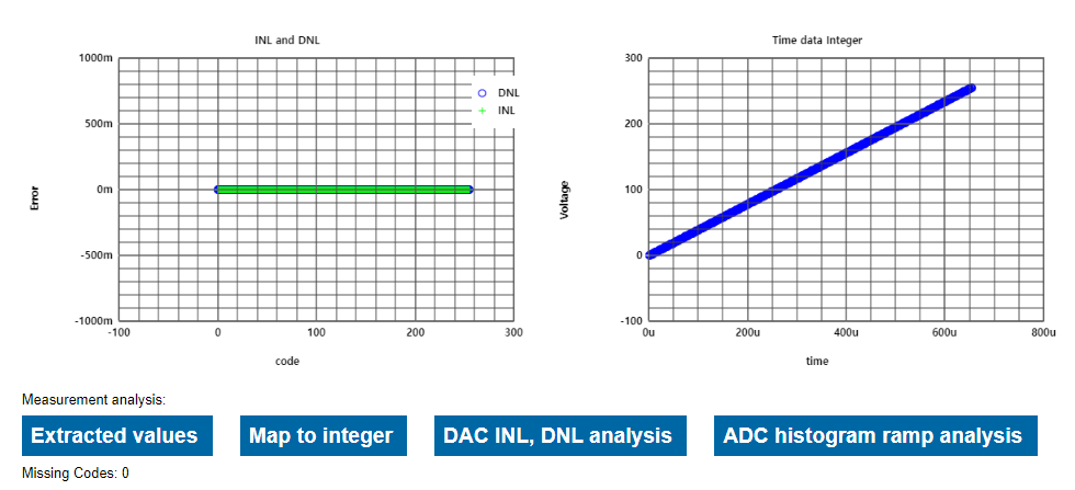
8 bit R2R DAC built in LTSPICE but Vout had no ramp so increased the period of pulse input for D,4,5,6,7.
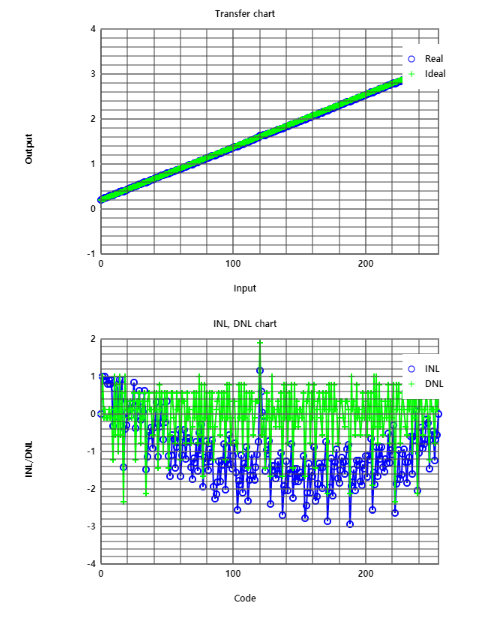
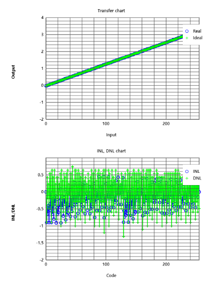
INL,DNL in ADC historgam range 0 and also missing code 0.
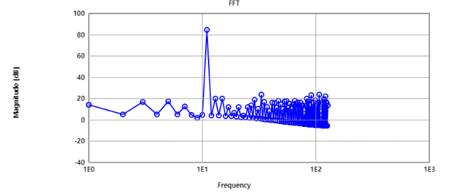
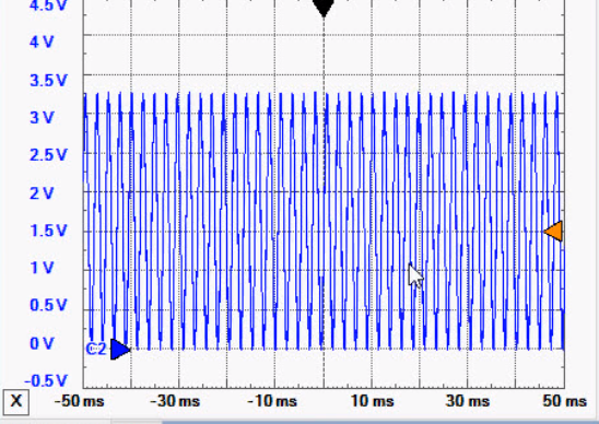
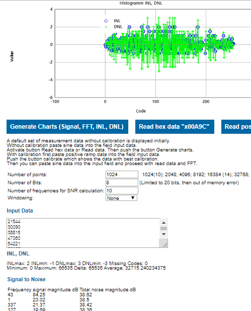
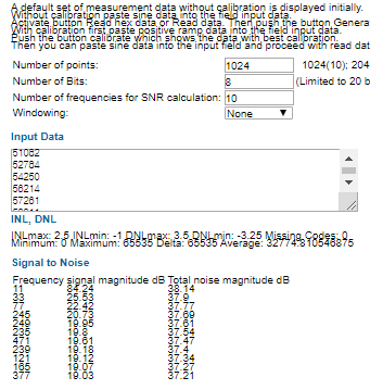
Sine test
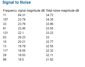
Siganl magnitude is 84.31dB, total noise is 34.72.
SNR=84.31 - 34.72 =49.59dB.
ENOB= 49.59-1.76/6.02 = 7.94.
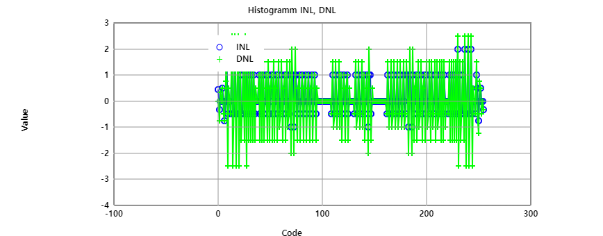
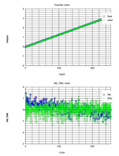
INL,DNL in historgam range -2~2 and missing codes are 140.
Changed more samples per code(step time)but there are always some missing codes.
Experiment #2 Breadboard R2R DAC
Setting
Set up a real 8bit R2R DAC on a bread board.
Resistor values measured by multi tester.
R1=200.2 R2=200.5 R3=200 R4=199.8 R5=200.1 R6= 199.9 R7=199.7 R8=200.4 R9=199.7
R10=99.5 R11=100.2 R12=100 R13=99.9 R14=99.8 R15=99.8 R16=99.8.
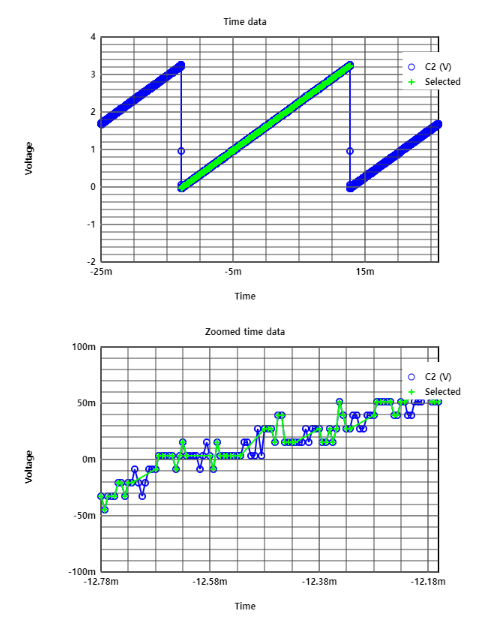
Binary counter pattern
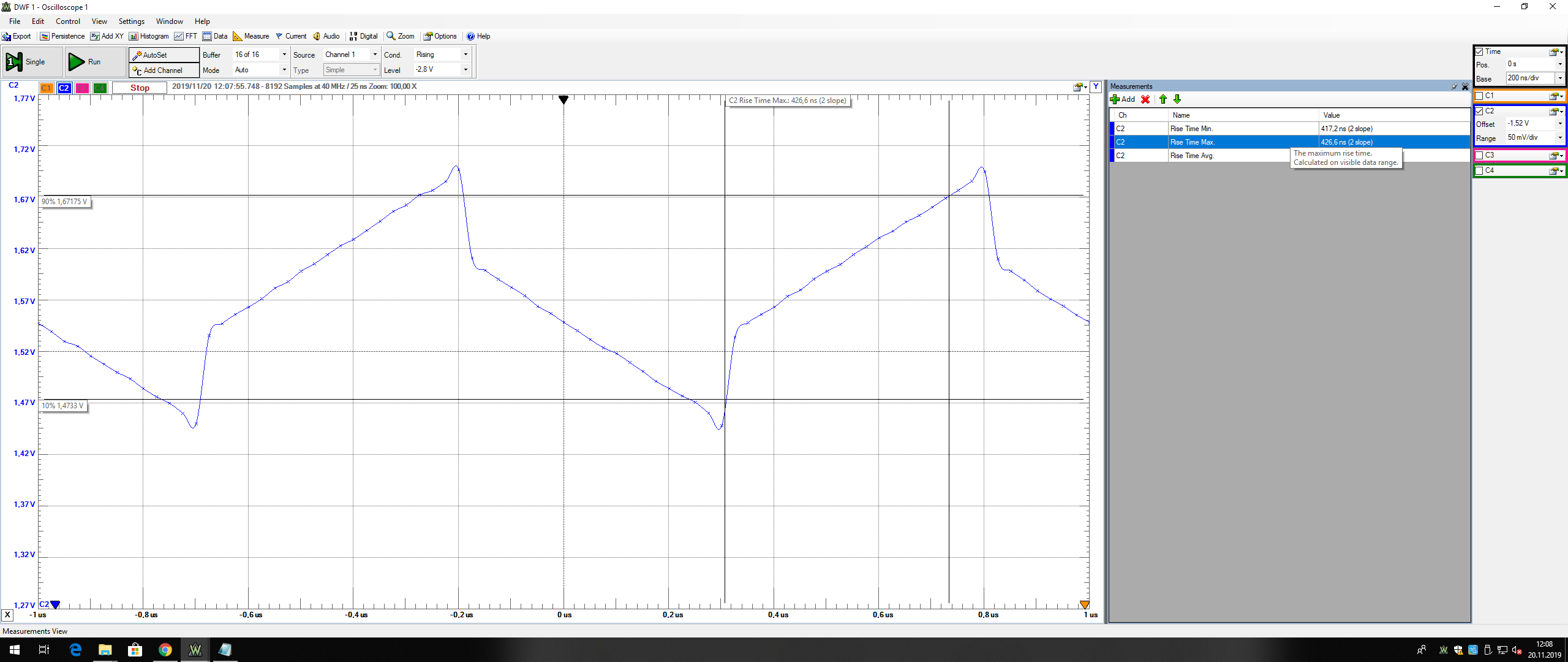
Low frequency 10kHz should be considered since it was difficult to have a good sawtooth curve more than 10kHz.
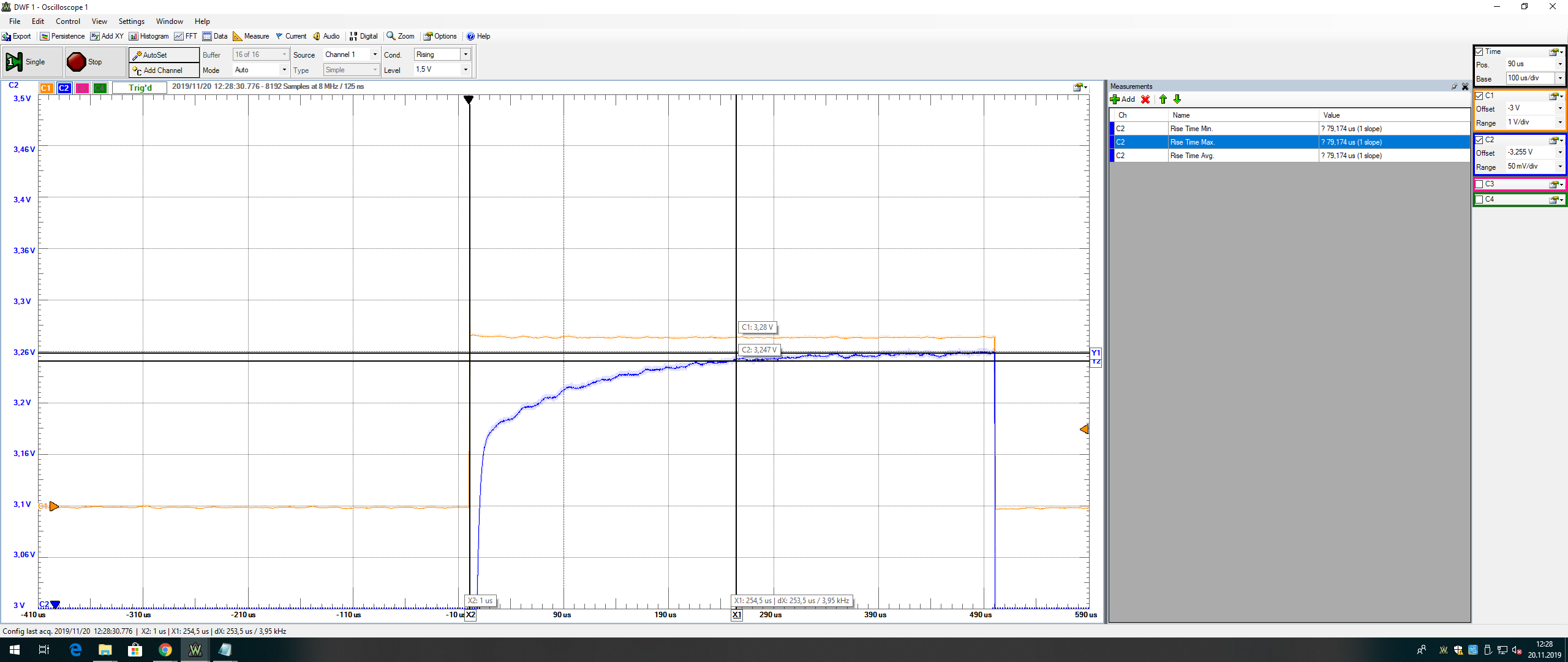
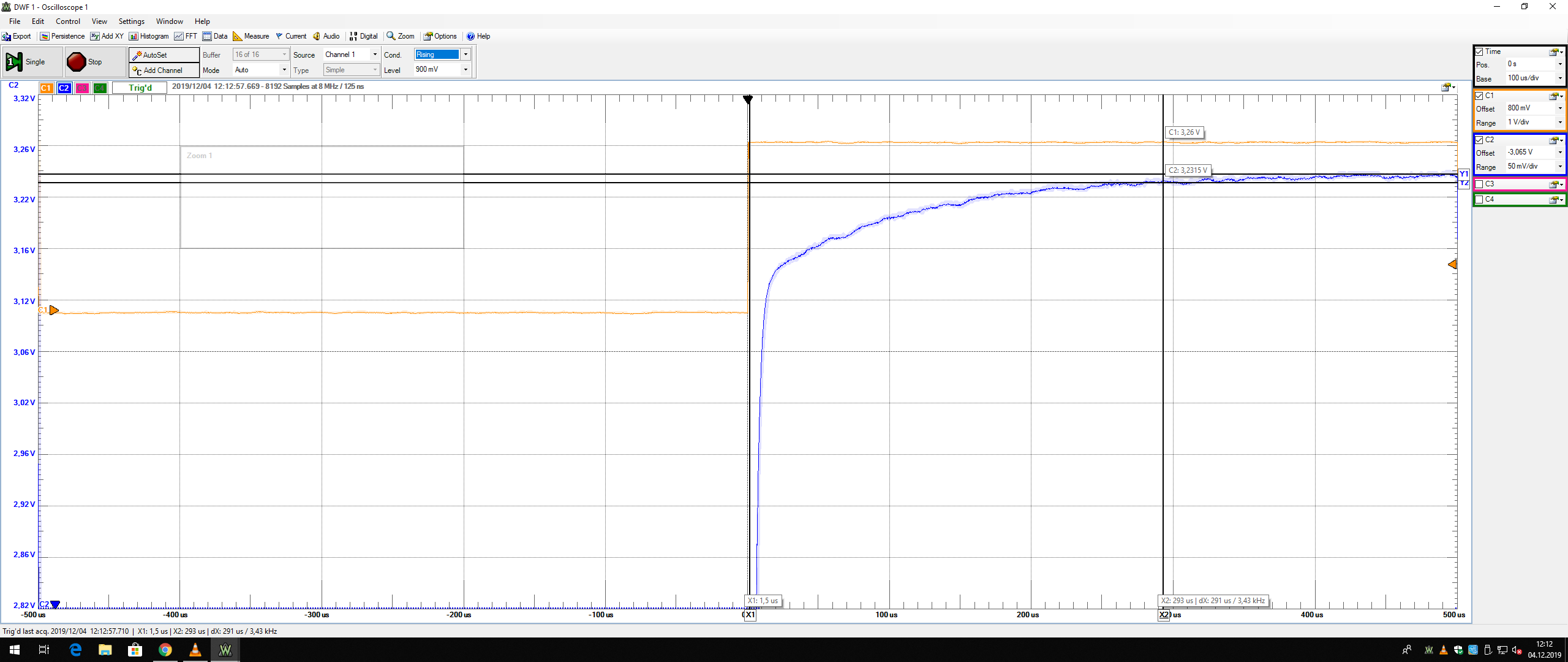
Offset voltage:-3.255V, Maxium voltage:3.26V, LSB=3.25V/256=12mV, Settling time:253.5us, Noise Vout: appox. 3.25V.
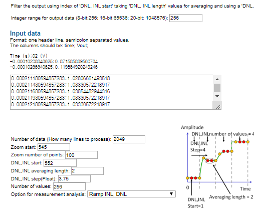
Measurement of INL,DNL
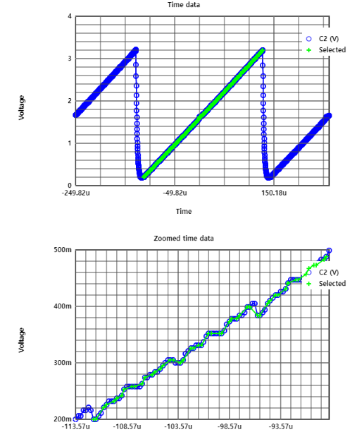
10kHz is the best frequency since higer frequency has the small number of data
and it was very hard to meausre DNL,INL and the values are too high.
10kHz frequency seems to be better than 1Mhz.
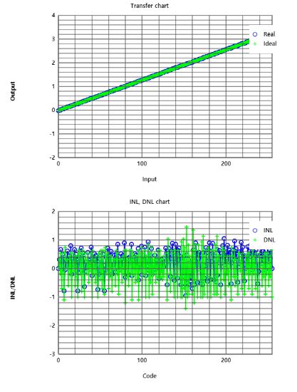
At 10kHz INL,DNL range is from -1 ~ 1 /at 1MHz, INL,DNL range is from -3 ~ 2
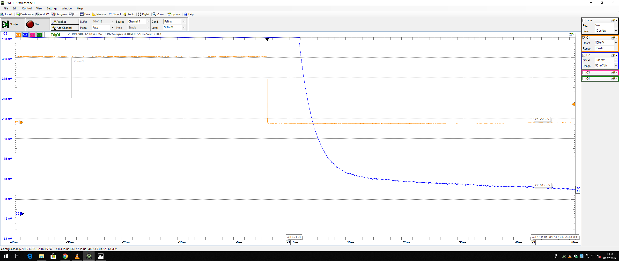
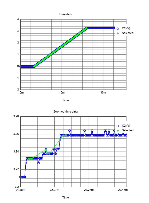
Experiment #3 Settling time of R2R DAC
-Signal voltage level here is 0v to 3.3v due to electronic explorer level of logic bit
-now for measuring Rise time we have to trigger for rise time. Our step size is 3.3/256 =15mV
-For this we have to zoom in for seeing the reaching level.
-similarly for measuring Fall time we have to trigger for fall time
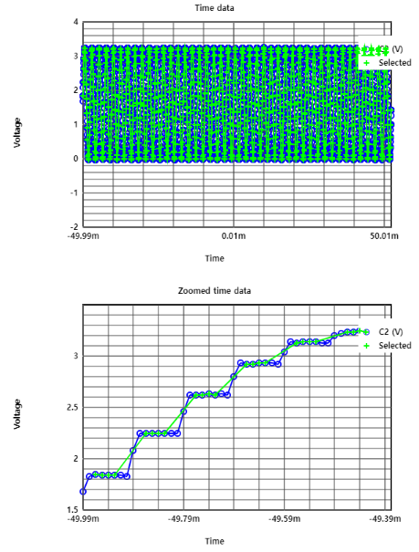
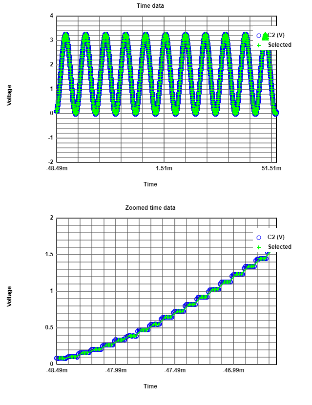
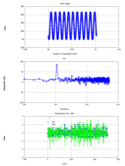
Experiment #4 Sine measurement of R2R DAC
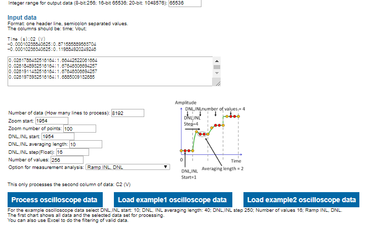
-For 43 period of sine signal we export data
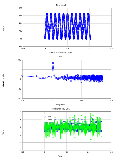
-after processing osciloscope data we have to process around eight thousand values
-after zooming we can see INL and DNL , we have to choose so that 4 values are remain per sample
-As we have positive and negative both value for sine measurement, we will now map it to positive integer data
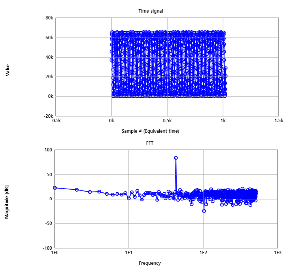
-Now we will go for FFT processing
-After FFT Processing we can see our nice signal without FFT
-From INL DNL we can see bit from 0 to 256
-DNL goes somewhere from -3 to +3. So there is a possibility to lose some bit
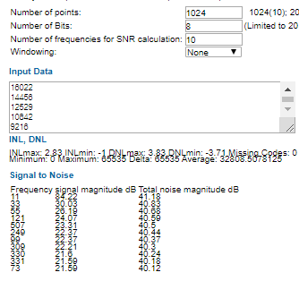
Experiment #5 Sine measurement of digital calibrated R2R DAC
Ramp calibration
Before the calibration INL,DNL range -1.5~ 1.5, missing code 189.
After the calibration INL,DNL range -1.5~1.5, missing code 190.
There is no development for INL,DNL and it does not seem to achieve good result.
Sine calibration
The calibrated sine signal deteriorated worse.
Total noise and harmonic values were getting higer.
As it is above, the signals are not impoved.