It started with the measurement of the ohmic resistances
with the help of a digital multimeter.
The results of that measurement is shown in table 1.
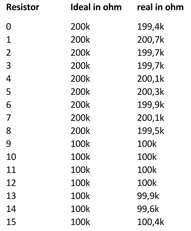
Table 1
After these resistors had been measured,
they were mounted on a so-called bread board.
The construction how it looks is shown in the following picture.
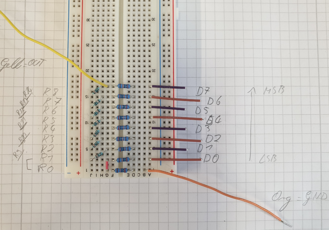
Figure 1
In order to simulate a real development process,
a model of the 8-bit DAC was generated using the LTSpice software.
With this model it is possible to detect possible errors at an
early stage and to correct them without material costs.
The process to develop the LTSpice model was as follows:
- Build 8-Bit DAC in LTSpice
- From this a symbol was created
- Then two 4-bit ADC's are linked and connected to the finished DAC symbol.
The developed model is seen in figure 2.
The reason for this approach was to visualise a possibility of comparison
between an analogue input and an analogue output signal.
This makes it possible to graphically determine the quality of the simulated DAC.
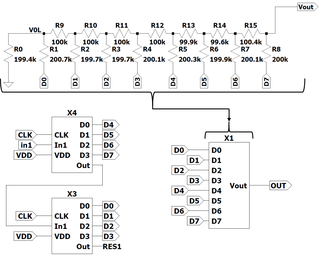
Figure 2
The next step was to subject the generated LTSpice model to a
so-called ramp test, in which a ramp selected by us serves as the input signal.
This ramp can be seen in the following picture.
The result is that the ideal ramp in green and the measured ramp in blue are largely congruent.
As you can see in Figure 4.
This made it possible to use the resulting output signal to determine
and evaluate the INL and DNL using Professor Vollrath's FFT website.
(https://personalpages.hs-kempten.de/~vollratj/InEl/FFT_Javascript_2017_Calibration.html)
The result of the INL, DNL process is shown in Figure 5.
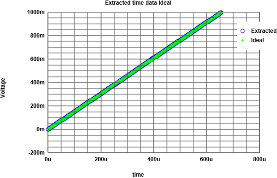
Figure 4
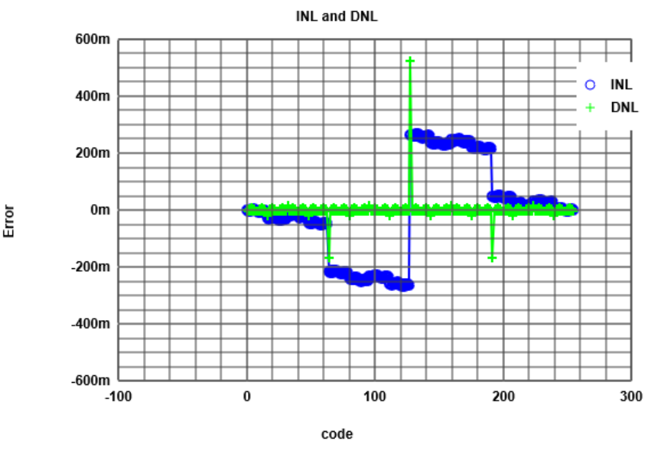
Figure 5
Looking at the INL and DNL it can be seen that the INL contains three significant jumps.
The reason for the two negative jumps, which are about half as large as the positive jump in the middle,
is an increase in the resistance value compared to the optimum value in the middle of the transducer.
We explicitly assume the cause to be the component deviation of R5, which represents the value D4.
The large jump, which can be seen centrally in the graph,
refers to the deviation from R8, which reflects D7 and at the same time represents the MSB.
Globally, this INL analysis is satisfactory as it is never available via ˝ LSB.
This means for the conversion the full bit width without losses is available.
In addition, Figure 6 shows an FFT analysis of the output signal.
With this analysis the so-called Signal to noise ratio (SNR) can be read from the generated Table 2.
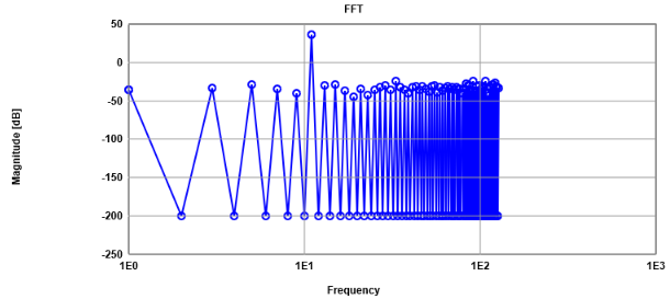
Figure 6

Table 2
The Signal to noise ratio at the Frequency 11 is: 36.12-(-13.45) = 49.57dB
This distance is very good and sufficient for our purposes.
So, we could start with the next point.
In order to verify our simulation, we examined the setup using a development board,
that provides both an oscilloscope and various signal generators.
In order to examine the signals, the output signal of the DAC was connected to the digital oscilloscope
(on Scope 2DC) with outdoor cabling wires. The input of the digital analogue converter
was connected to the digital output 1 of the board (ScopeDC1) with a wiring harness.
This structure is shown in the following figure.
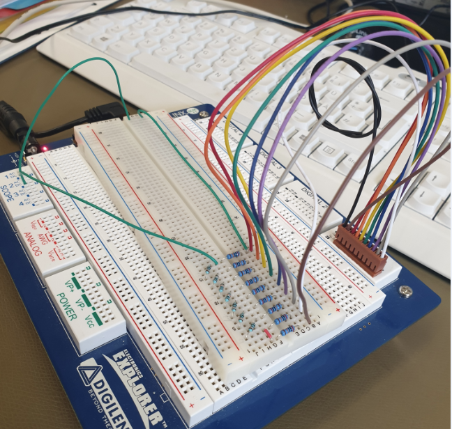
Figure 7
The corresponding software of the development board was started and adapted to our needs.
This enabled us to use all oscilloscope data and signal generators.
For example, the implementation of a digital bus system (DI0...DI7).
Real data Measurment of our DAC
The measurement of the offset voltage resulted in a value of -7.5mV.
For this measurement we don´t provide any picture,
because it is quiet easy to measure it. You switch on the DAC and give a zero vector as an input.
The output voltage you could measure then, is the so-called offset voltage.
This value is not so bad, because it is lower than one LSB level.
The measurement of the LSB can be seen in Figure 8: and shows a voltage of nearly 11.7mV
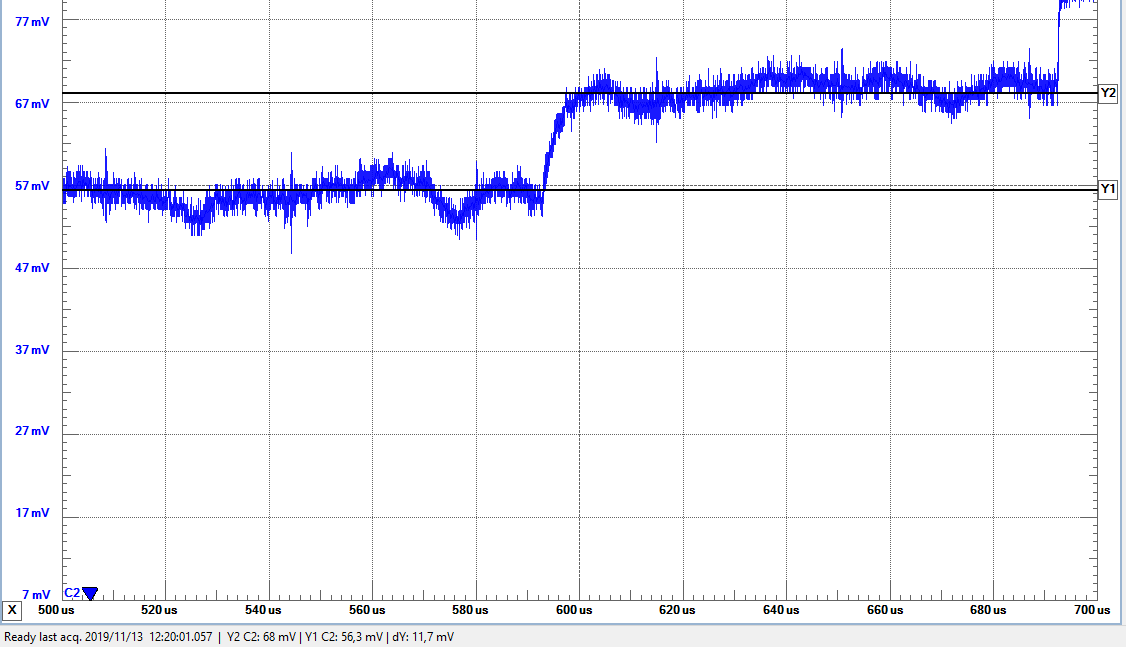
Figure 8
Because we are using a 8-Bit DAC, 256 values are expected.
The maximum voltage can be calculated as follows.
V_max = 256*LSB+V_offset = 2.9945V.
To determine the parameters of the DAC, the maximum voltage V_max, the LSB, the offset voltage,
the full-scale setteling time (t_set_full) and the mid-scale setteling time (t_set_mid) were measured,
t_set_full is the time the DAC needs to jump from 0 (00000000) to 255 (11111111).
t_set_mid is the time it takes the DAC to jump from 127 (01111111) to 128 (10000000).
The results of this measurement are as follows: V_max = 3.235V; t_set_full = 15us; t_sett_mid = 17.5us.
The difference between the measurement and the calculated value for V_max l is due to measurement inaccuracies.
The following pictures shows these values.
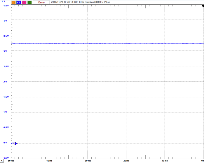
Figure 9 (V_max)
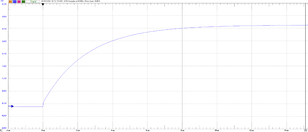
Figure 10 (t_set_full)
Full settling time rise = 15 us
Full settling time fall = 12.9us
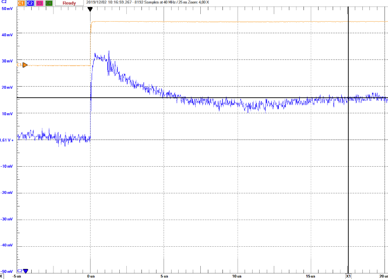
Figure 11 (t_set_mid)
Mid settling time rise = 17.5us
Mid settling time fall = 13.3us
All these values are acceptable.
If the clock frequency is increased, the settling time increases. This has the consequence that
from a frequency of 45kH the desired value is no longer reached when jumping from 0 to 255.
Evaluation of measured data
In order to investigate the frequency dependence of the built-up DAC, different frequencies
of the signal were applied to the R2R DAC and those measured with the oscilloscope.
The data were read and processed with the help of the Read-oscilloscope-webpage of Professor Vollrath
(https://personalpages.hs-kempten.de/~vollratj/InEl/ReadOsci.html).
We have made measurements at the following frequencies:
F = 10MHz; F = 1MHz; F = 100kHz; F = 10kHz
The pictures show the FFT analysis, at a frequency of 10kHz (Figure 12) and 10MHz (Figure 13).
Immediately it is noticeable that the INL at the frequency of 10MHz is much higher than at a frequency of 10kHz.
This has to do with the settling-time. If the frequency is too high, the DAC no longer follows with the conversion.
This results in a code loss. For this reason, we have chosen a frequency of 10kHz.
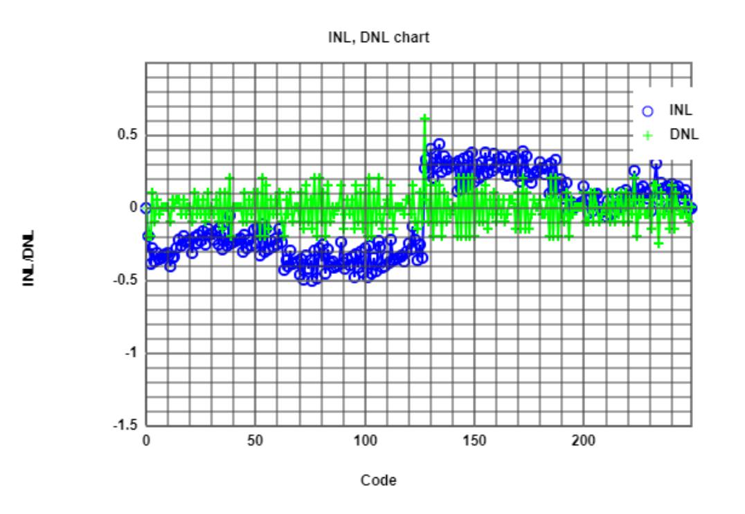
Figure 12 (f=10kHz)
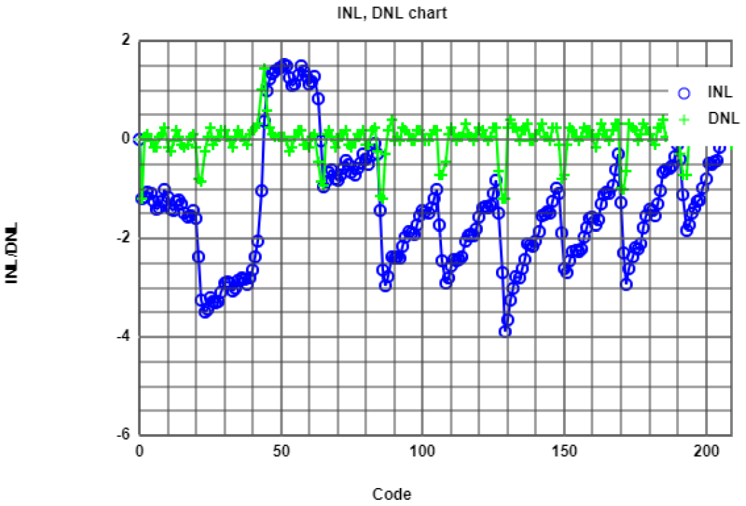
Figure 13 (f=10MHz)
|
Improving the 8-Bit R2R DAC by changing a resistor
As you can see on the picture of the INL and DNL analysis of the 10kHz signal (Figure 12),
the largest INL value is in the middle of the graph. This is because the MSB is set at
exactly this time. A deviation of the resistance in this branch will result in this spice.
For this reason, we have decided to exchange this resistance (R8).
The initial value was 199,5kOhm and was replaced by a resistor with the value of 200,0kOhm.
With this change it is possible to push the INL to a maximum of roughly 0.2 LSB. This you can see in figure 14.
Figure 14
|
|
Real data Measurment of our improved DAC
After the implementation of the improvement, a digital sinusoidal signal was now converted.
The digital sinusoidal signal with 43 periods was available for downloading by Professor Vollrath under the link
(https://personalpages.hs-kempten.de/~vollratj/InEl/10Bit_Sine43Periods.csv)
The signal can be seen in the following picture.
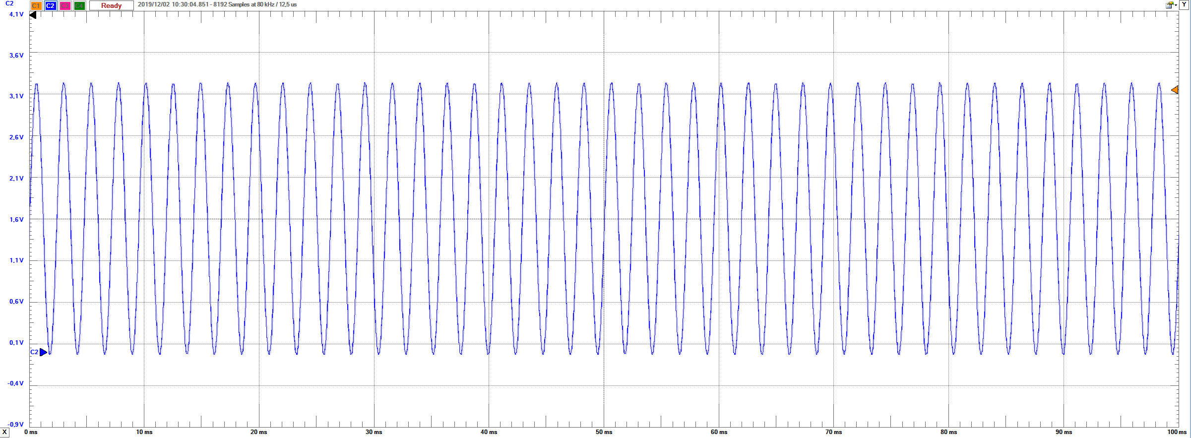
Figure 15
The measured oscilloscope data were converted with the Read_Osci webpage.
The generated values were then converted and examined with the FFT_Analysis of the sine function tool.
(https://personalpages.hs-kempten.de/~vollratj/InEl/FFT_Javascript_2017_Calibration.html)
When you are looking at the FFT plot, the sinusoidal frequency is clearly visible.
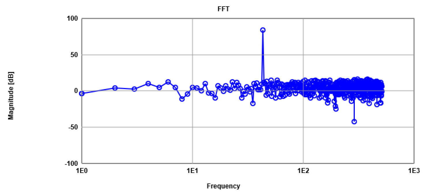
Figure 16
The following table shows the frequency of our digital sinusoidal signal.
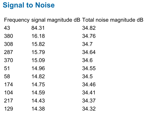
Table 3
The signal to noise ratio is 84.31 - 34.82 = 49.49 dB.
So, this one is very good.
Improving the 8-Bit R2R DAC by digital calibration
The digital calibration did not show any improvement in our case.
On the contrary, the increase of the INL via ˝ LSB is clearly visible in the next picture.
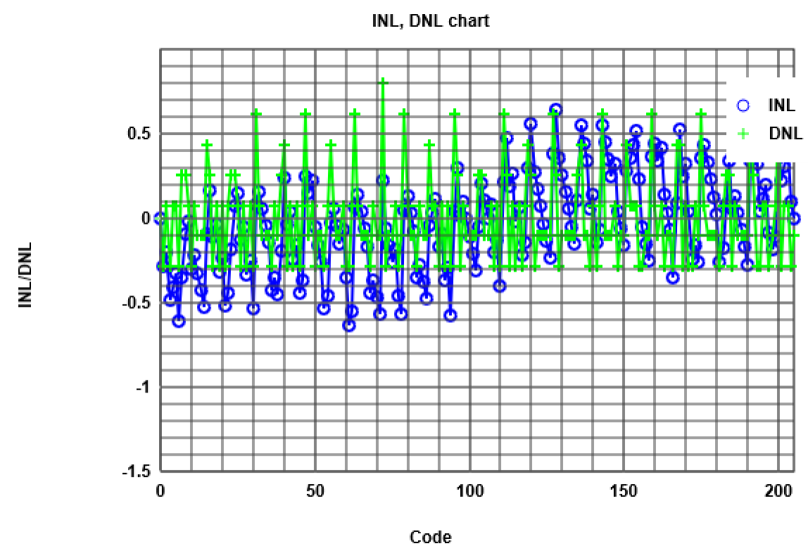
Figure 17
In our case we are not currently sure, if the calibration is correctly done.
The INL should decrease by implementing digital calibration.
Time was the limiting factor. For this reason we were not able to repeat the digital calibration.
Luckily our INL and DNL without calibration is also acceptable.
Conclusion and Time
Conclusion
- This laboratory was perfect to see the difference between real world applications compared to theoretical apps.
- Furthermore, it was fantastic to built up our own DAC from skretch.
- Moreover, we learnt a lot how real devices act in a circuit and how sensible the DAC reacts with little tolerances of components.
- One drawback was, to get used to the digital oscilloscope software.
- To sum up the conclusion, we are still satisfied with our results.
Time
- The time required to do this laboratory was enormously.
Also many additional hours had to be spent in the laboratory to perform all measurements,
so that the deadline of the laboratory report was not endangered.
- To sum up, we can say that this laboratory was very
time-consuming for our group, in detail more than thirty-five hours.
|
|
|