R2R DAC LTSPICE Simulation - 600K
In Lab 04 we are going to examine an R2R DAC. The charm of this DAC type is that only two different types of resistors are needed.
During lecture we called them "R" and "2R" which also gives this DAC type its name.
To get started we set up an 8 bit R2R DAC on a bread board.
In parallel we create a schematic in LTSPICE to observe the behaviour of our DAC.
R2R DAC on a bread board - 600K
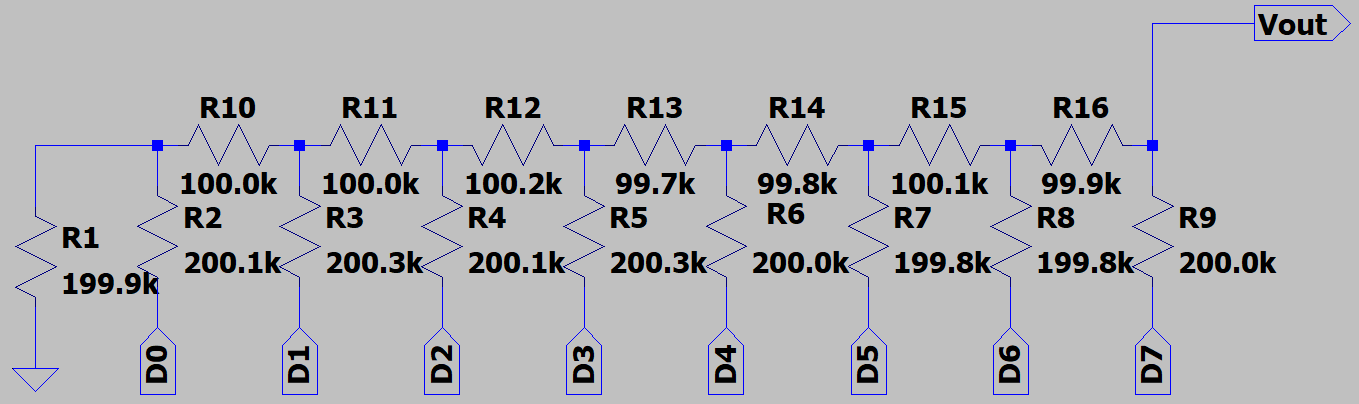
The two types of resistors we use are 100k (R) and 200k(R). In the picture we can see the result.
The nine darkblue resistors placed between the two parts of the breadboard are the 2R resistors.
The white and brown cables symbolize the data pins D0 to D7 starting from right to left (LSB to MSD).
The completely on one side of the breadboard placed lightblue ones are the R resistors.
The black cable will be used for a connection to ground later in the lab.
.PNG)
Set up of an 8 bit R2R DAC on a bread board
R2R DAC in LTSPICE - 600K
The R2R DAC build on the bread board is now modeled in LTSPICE.
To be able to make a more realistic simulation the before measured resistance values are used for the resistors.
Schematic of R2R DAC in LTSPICE
In the past we were working with a LTSPICE model of an ADC.
After we created a symbol out of the R2R DAC we put the ADC and DAC together in one LTSPICE schematic. The schematic is shown in the picture underneath.
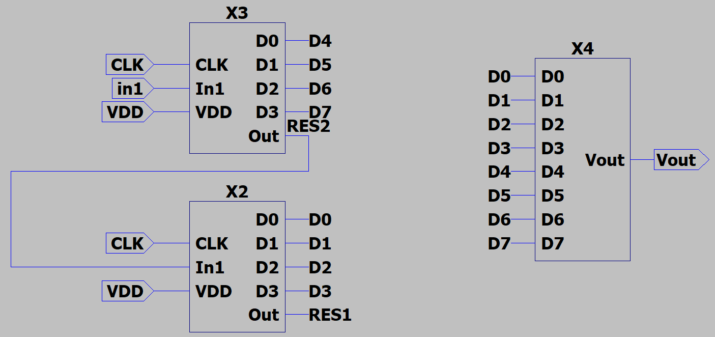
Schematic of R2R DAC symbol and an ADC used in past lectures in LTSPICE
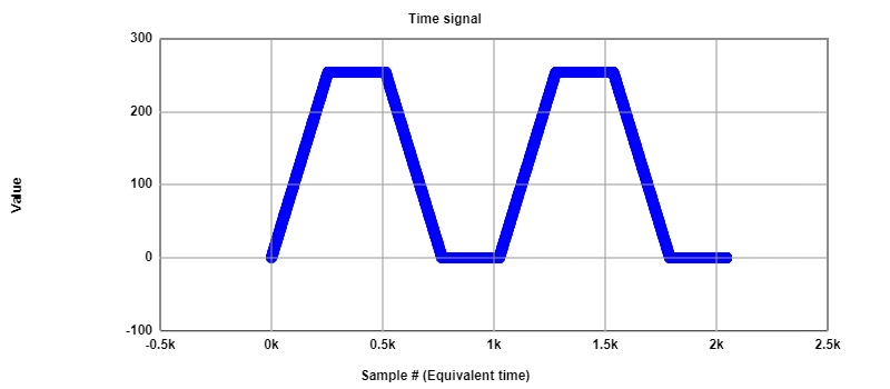
Simulation with a ramp input signal - 600K
The complete duration of the simulation 655.36 us. The result of the simulation is shown in the picture underneath.
For further analysis the output V(out) displayed in the picture is saved in a log file.
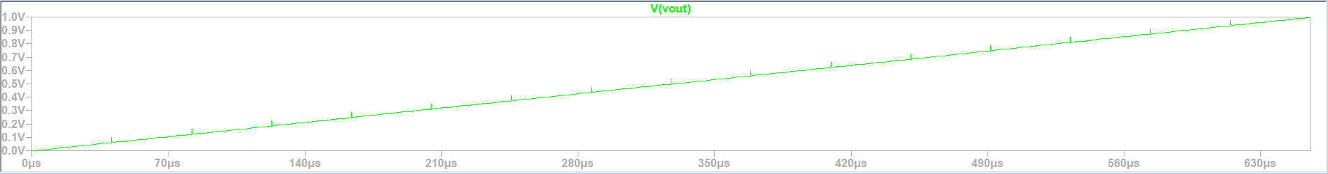
Simulation in LTSPICE with a ramp input signal
The logged values will be used for further analysis. With the help of the "ReadRawFile"-Tool we will take a look at the INL and DNL error.
The filter in the tool will be configured as follow:
Start time: 0
Stop time: 655.36 E-6
Time step: 2.56 E-6
We want to analyze to complete simulation. To do that the start and stop time is set over the whole duration of the simulation.
The step size is 2.56 us. To analyze the DAC we want to have a measurement point at each of the 256 levels of voltage.
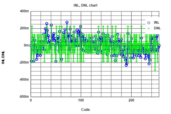
The graph of the ideal and real curve doesn't give us further information. At least we can say that we can't see a difference with such a resolution.
The graph of the INL and DNL error gives us more things to discuss about.
Most of the time the INL and DNL error is less than 0.05 which is a really good result.
From code 60 to approximatelly 127 the INL error is higher than at the start. After that reagion the INL error switches to same level but in negative values.
For nearly the last 60 code the error is again very low for INL and DNL.
I would assume that our DAC is not very good for signals at the D3 to D6 cause of the higher error occurencies in the middle.
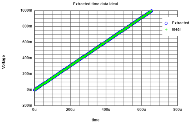
Real and ideal curve of the simulation. |
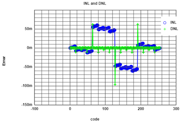
INL and DNL error of the simulation. |
Simulation with a sine input signal - 600K
This simulation with a sine input signal is done with the same schematic as the simulation with the ramp input.
In the picture of the simulation output (V(out)) we can see eleven periods.
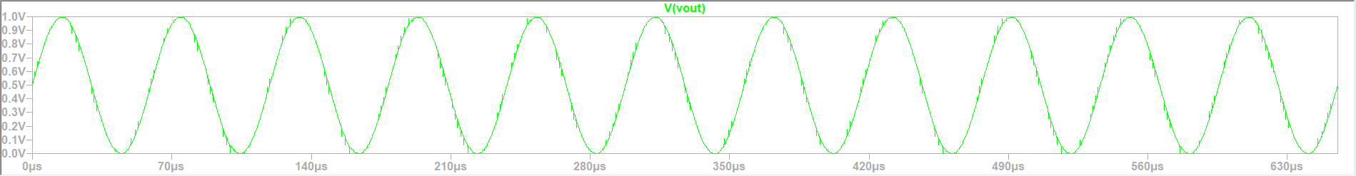
Simulation in LTSPICE with a sine input signal
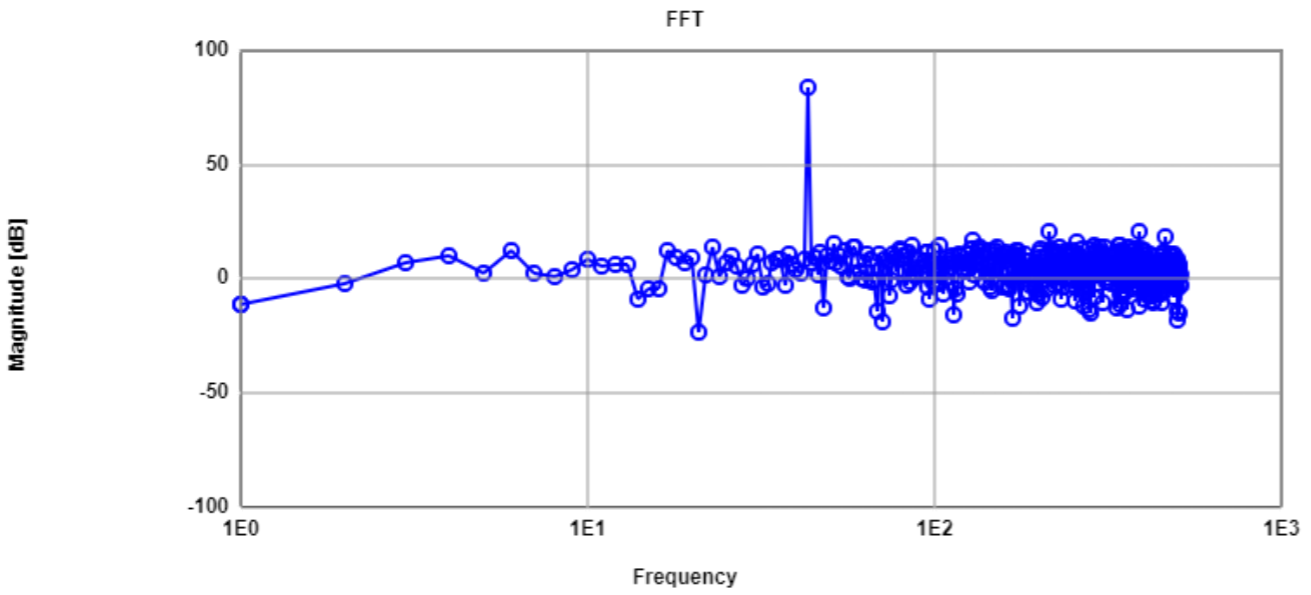
For the FFT analysis we used the "FFT analysis"-Tool. The first step was to use the "ReadRawFile"-Tool to filter the values.
We used the same filter configuration as in the ramp simulation analysis. After mapping the points to 256 integer values we inserted the them into the "FFT analysis"-Tool.
The FFT analysis wasn't satisfying. It looked extremely different to any other FFT I saw from a sine signal. I decided that a discussion/analysis about it would be useless.
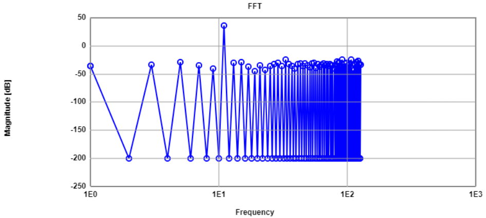
FFT of sine input signal simulation. |
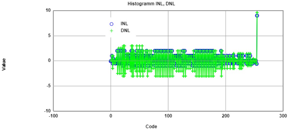
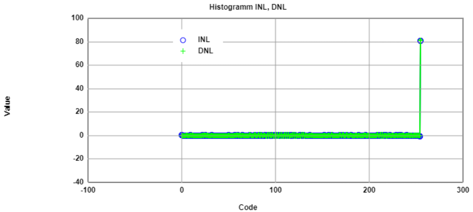
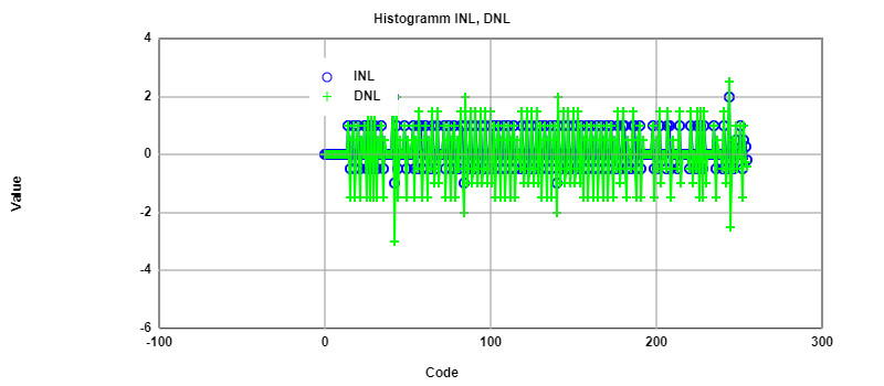
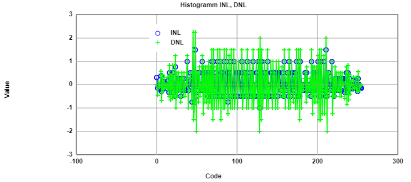
Histogramm of INL and DNL error. |
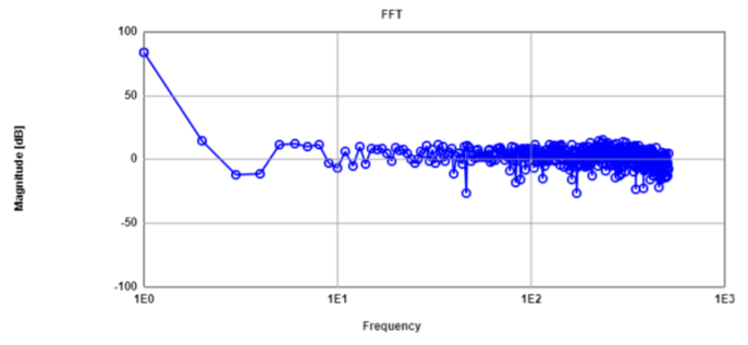
This time I changed the filter configuration of the "ReadRawFile"-Tool. The start and stop time are remaining the same, but to get more points I changed the step size.
The new configuration for the filter is as following:
Start time: 0
Stop time: 655.36 E-6
Time step: 0.36 E-6
By changing the step size to 0.36 us we get more points per code. The total amount of points is now 2048.
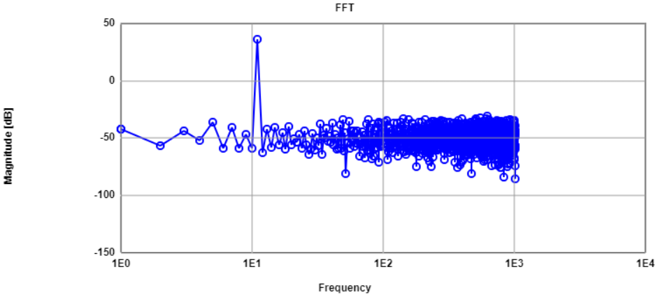
After inserting those filtered values to the "FFT analysis"-Tool we get the FFT as displayed in the left picture underneath.
We already know the following out of our simulation with a sine signal input:
8 bit ADC connected to an 8 bit DAC
complete measurement time: 655.36 E-6
amplitude of output sine signal: 500 mV
number of periods: 11
What we can read out of the FFT:
signal magnitude at frequency 11: 36.12 dB
total noise magnitude at frequency 11: -13.67 dB
We miss the view of harmonics.
INL and DNL error looks really bad. We assume the reason lies in bad configuration and input values of the FFT tool.
What we calculate with approximated equations out of the lectures:
signal magnitude:
\(20 \log{\frac{0,5}{\sqrt{2}}} = -9 dB\)total noise:
\(-9 dB - 6.02 \times 8 dB -1.76dB = -58 dB\)noise distribution (cause of the 2048 bins):
\(-58 dB -10 \log{256} dB = -82 dB\)
FFT of sine input signal simulation. |
Histogramm of INL and DNL error. |
R2R DAC Breadboard - 419L
Test setup
The setup on the breadboard is the same as in the simulation in LTspice. Only extra wires for the oscilloscope are necessary.
In the figure below all wires are connected. The red circle shows the real output digits of the pattern generator.
On the right hand side of the resistor network, LSB is located and on the third wire from the left side the MSB. The two left wires from the output block are ground connections.
Channel one of the scope is connected to the output of the DAC. The output is situated between the two left resistors.
The second channel is used as trigger of the osziloscpoe. It is conneced to MSB / D7 of the DAC.
A further explaination of the resistor network can be found in chapter "R2R DAC LTspice Simulation".
.jpg)
Breadboard connection with pattern generator and osziloscope
Ramp test
To analyse the connected DAC a standard ramp test is done. Therefore the digital outputs zero to seven are selected as bus.
First the oscilloscope and the pattern generator have to be started. This is shown in the picture below. The necessary windows are surounded red.
Necessary program windows
After selecting this windows the following windows occure. On the left side you see the oscilloscope, on the right side the pattern generator.
Both need to be configured separatly. The configuration is dependend on the tasks and have to be changed frequenty.
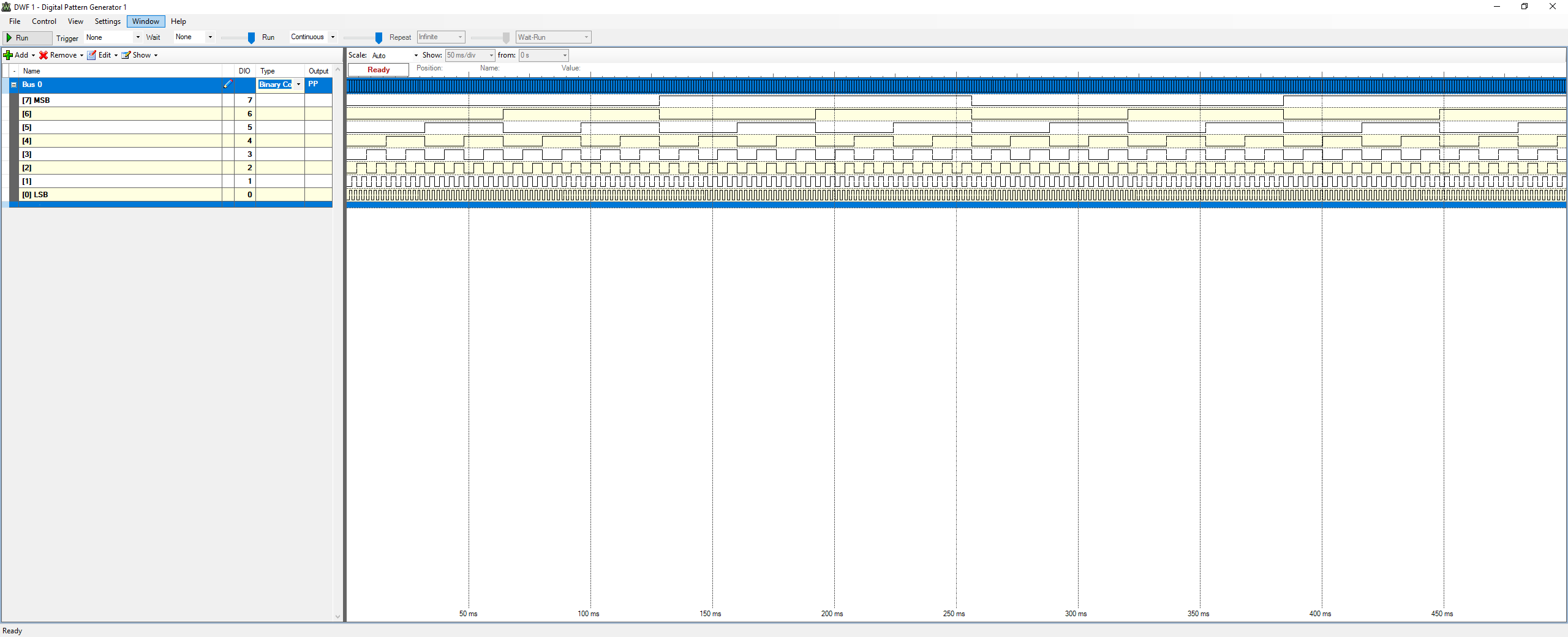
oscilloscope and pattern generator
A ramp can be generated by a binary counter pattern. As result a rising ramp is fed into the DAC.
In the following picture the measured signal on the osziloscope is shown. The steps of the DAC are only visible if you zoom further into the picture.
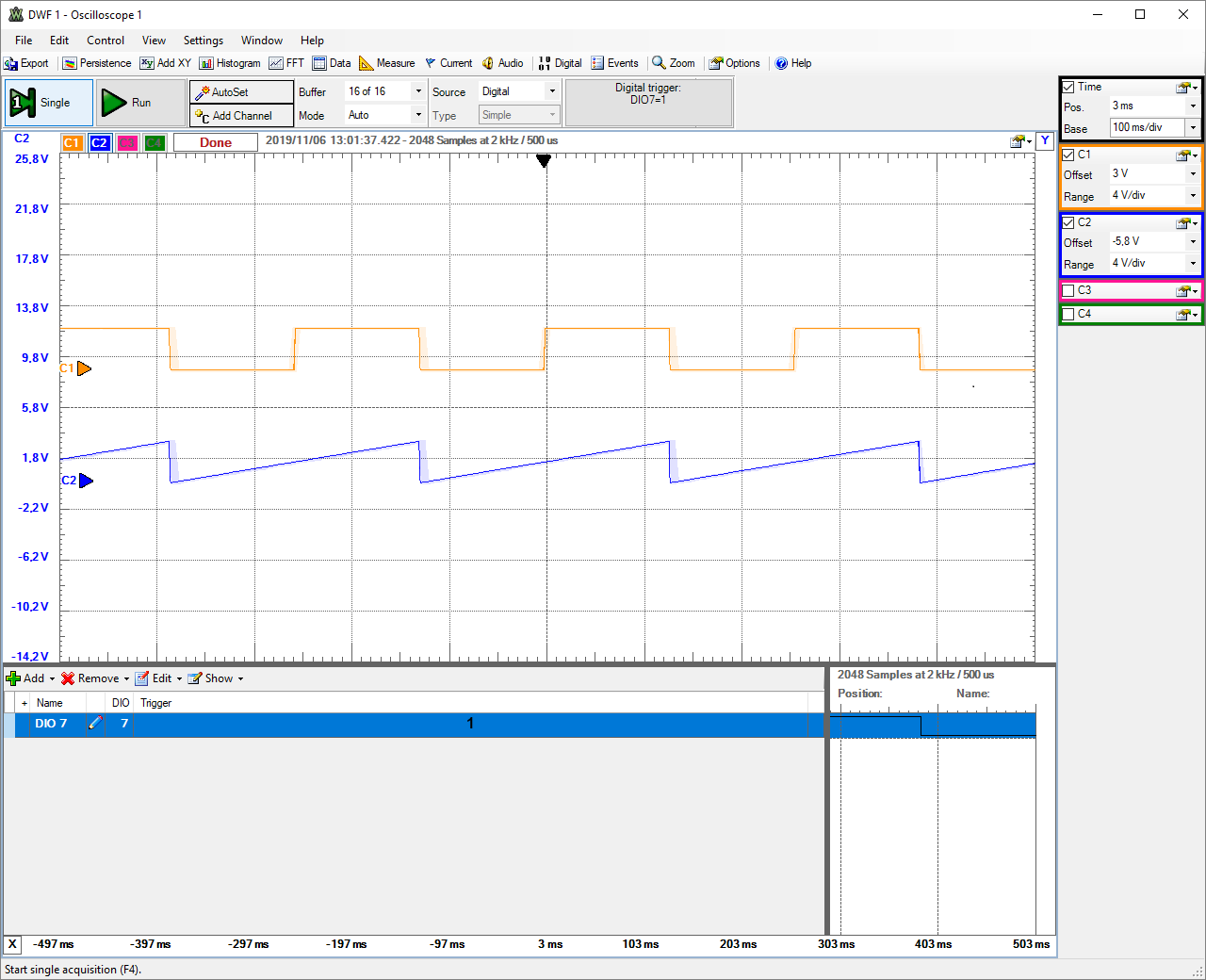
Output ramp and trigger signal D7
To analyse the DAC further all values are exported and put into the webpage read oscilloscope data. There it is possible after configuration to calculate INL and DNL.
During configuration it is necessary to set the beginning of the calculation just before the ramp starts to rise.
LSB and MSB
To read out LSB it is necessary to use a small voltage per devision and zoom into the picture. Since the step size should be always the same size, we measured somewhere in the middle of the ramp. This is not always the case. It is better to measure at the beginning of the ramp. Right now we do not know if we measure a change from LSB from 0 to 1 or maybe a nother bit is changed and LSB is turned off. We only measured the step size but not the least significant bit.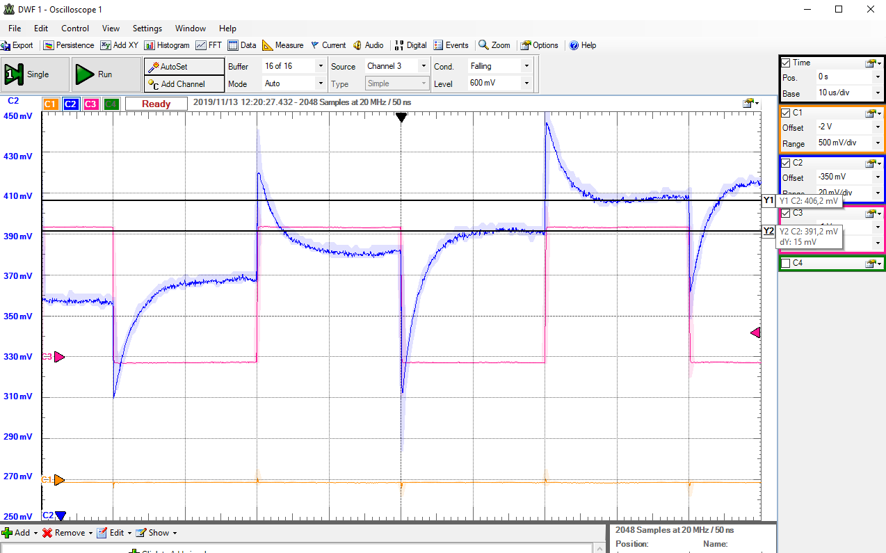
Measured step size
To measure the voltage level of MSB it is necessary to look at the code 128. There only MSB is turned on and all other bits are zero. To get this step it is recommended to use the trigger on D7. Since we worked with 50kHz, an overshoot occurs which decrease over the sampling time. Our MSB has a value of around 1.617V.
Measured MSB at code 128
Frequency configuration
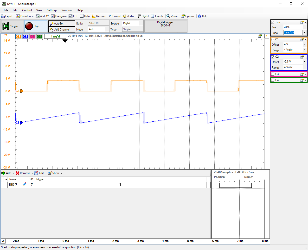
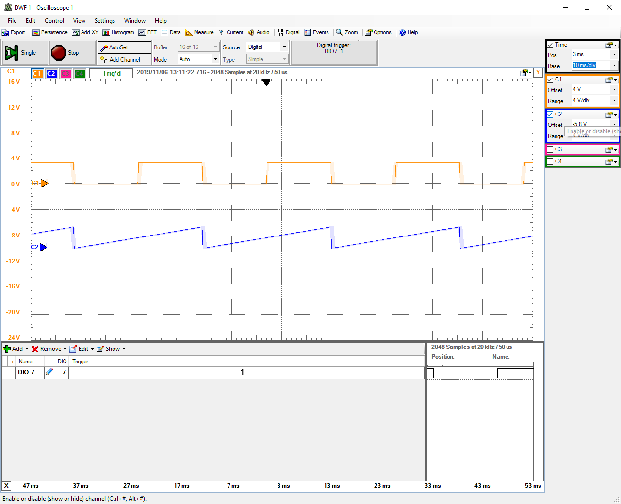
The patern generator is able to work on different frequencies. Our DAC is bandlimited. To select the best frequency for the application of our DAC, the frequency is varied between 10kHz an 10MHz.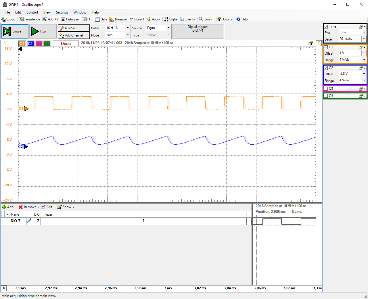
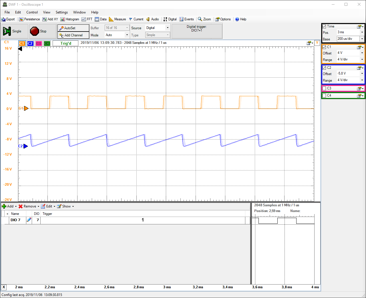
Pattern generator with 10MHz left and 1MHz right
Pattern generator with 100kHz left and 10kHz right
It is visible that at higher frequency the low values never are reached. The voltage needs more time to reach 0V. Therefore further investigations are done with the lowest frequency (10kHz). The resistor network shows an capacitive characterisic at high frequencies.
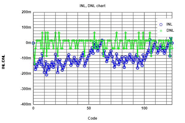
For using the INL and DNL tool only one ramp needs to be analysed. Therefore the exported signal has to be cut. Since we were unable to use the tool on the website without further intruduction, we cut the exported data by searing for run ramp in the csv-file. One problem which was fixed later is the export of only 2048 values and not 8192. This reduce the resolution of the oscilloscope. Bellow the measured INL and DNL is shown and the automatic choosen input parameters. A look on the graph shows that INL and DNL are always between +-0.5 which is a good result.
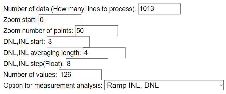
Left side selection, right side result in INL and DNL
To optimize the DAC we change the resistor on D3. This resistor has a value of 200.3kOhm which is the highest measured difference. Resistor R3 which is connected to D1 has the same value (look table in first section), but since it is close to LSB, its influence is small.
The new resistor R5' has a value from 200,1kOhm.
Since we were only allowed to change one value, we did not change the resistors on D6 and D5. Their deviation was lower, but their influence could be higher because they are closer to MSB.
The result of our INL DNL optimisation is shown in the figure bellow. We cut the data again while looking for the voltage drop in the raw data and not with the tool on the website.
While adding the changed data again on the website, the failures we made are visible immediately. The Data has only a size of 1014 lines. And since we did not change any value, the INL and DNL is calculated only above 126 points.
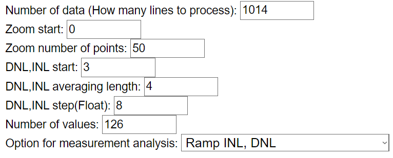
Left side selection of corrected R5, right side result in INL and DNL of corrected R5
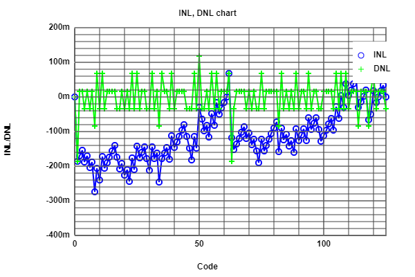
The values above show still a nice curve for the INL and DNL analyse, since all values are bellow +-0.5. The INL got worse and not better.
The calculation is done for a log2(126) = 6.977 bit DAC. The jump in the middle of the INL analyse indicates an influence of the MSB resistor.
Review after some weeks to chapter "DAC R2R Breadboard"
Although we always exported only a quator of the values, we were able to choose the correct frequency to analyse the DAC. The decision was done by looking at the oscilloscope graphs and comparing 10MHz with 10kHz.
The change on D3 still makes sense, since it had the highest deviation compared to other resistors. However a change on D6 or D7 could result in an decrease on INL and DNL. A real comparisment is not possible because we did not export enough data and got problems with our method of selecting the right data.
For measuring the settling time we used the helping lines of the programm.
In the left picture you can see the recorded voltage of the oscilloscope while triggering to the rising edge of D7 (MSB).
We took the trigger point of D7 as the start point of the time measurement.
For the second point we set the resolution of the oscilloscope high enough to find the first point after the overshoot and reaching a stable maximum voltage level.
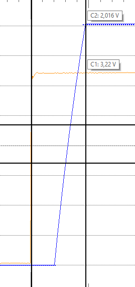
The overshoot after changing the output voltage from code 0 to 255 is shown in the right picture.
We ovserved the following in our measurement:
The measured settling time: 2.32 us
maximum voltage (blue line): 2.016 V
voltage at D7 (orange line): 3.22 V
overshoot when reaching maximum voltage: 350 uV
Settling time over to full range. |
Overshoot when switching over the full range. |
Settling time switching over one code - 600K
For the second test we again have to change the configuration in the "Pattern" Module. We change it to generate the following two codes.
The input voltage for D7 is negated to the other digital inputs:
0111 1111 (code 127)
1000 0000 (code 128)
In this test we are expecting a lower overshoot than in the previous test over the full range.
The voltage level at code 127 and 128 should be nearly half of the theoretical maximum voltage of 3.3 V.
Like the smaller size of the overshoot the settling time should also be smaller due to the smaller change of the output voltage.
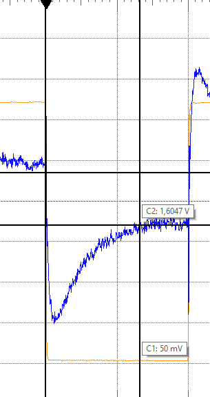
The measurement of the settling time is shown in the left picture.
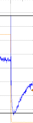
The overshoot is diplayed on the right side.
As starting point of the measurement we again using a trigger point of the input voltage of D7.
The second point is set until the voltage reaches a stable level.
The following we were able to ovserve:
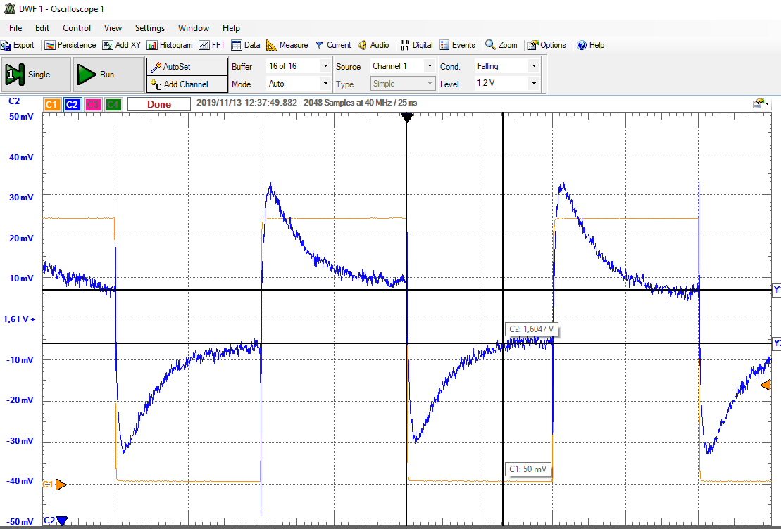
The measured settling time: 6.6 us
voltage at code 127: 1.6047 V
we have an compared under- and overshoot (right picture).
It first goes up to 1.6476 V and than down to 70.3 mV
Settling time over switching of one code. |
Overshoot when switching over one code. |
R2R DAC Sine measurement - 419L
Fast Fourier Transformation - Sine analyse
To analyse a sine signal on the DAC, the settings of the pattern generator has to be changed. Therefore the new video helps alot. during the lab we did not notice the necessary integer data input to the fft. It is again to mention that we only exported 2048 samples and not 8192.
After changing the settings as explained in the description the oscilloscope data is exported and put into the FFT tool. On the website two different sine signal files are available with a different number of periods. Both files contain 1024 lines of code which define the digital output in the pattern generator. Since one file consists of 43 periods and the pattern generator works with 10kHz, the real frequency of the signal is 430kHz. The second signal consists of only one period.
The following figures show the FFT analyse of the above descript signals. The x-Axis has a logarithmic scale. The values are dependend of the sampling frequency. Since this frequency is not include in the data, the values of the graph have to be multiplied by the sampling frequency to get the correct result.
FFT sine signals 43 periods
FFT sine signals one period
The first graph shows ate 43 a peak which indicates the calculated frequency from above. No other harmonics occure.
The second graph looks very different at the first view. There no clear peak is visible. It only starts on a high value at a frequency of 1E and runs against zero for all other frequencies. The multiplication with the samling time results again with the real frequency of 10kHz.
Since we worked with two different signals above (430kHz and 10kHz), we did not change the signal frequency again. We expect an increase of the signal to noise ratio (SNR) for higher frequencies and a lower SNR for lower frequencies. This assumption is based on the test, done in chapter two "R2R DAC Breadboard". The FFT curve on the website stays the same, if the export is done as in the analysis before.
The following table shows the resulting signal to noise ratio and the effective number of bits.
| Frequency | 430kHz | 10kHz |
|---|---|---|
| Signal magnitude in dB | 84.29 | 84.31 |
| Noise magnitude in dB | 34.89 | 32.21 |
| SNR in dB | 49.4 | 52.1 |
| Magnitude first harmonics in dB | 20.94 | 15.48 |
| Bits | 8.20 | 8.65 |
The bits are calculated by the formula bits = SNR/6.02dB. We did not lose a bit by this calculation. An increase of the pattern generator frequency would increase the noise magnitude which results in a lower SNR. The first harmonics magnitude is far bellow the noise magnitude. Therfore the number of bits is limited by SNR.
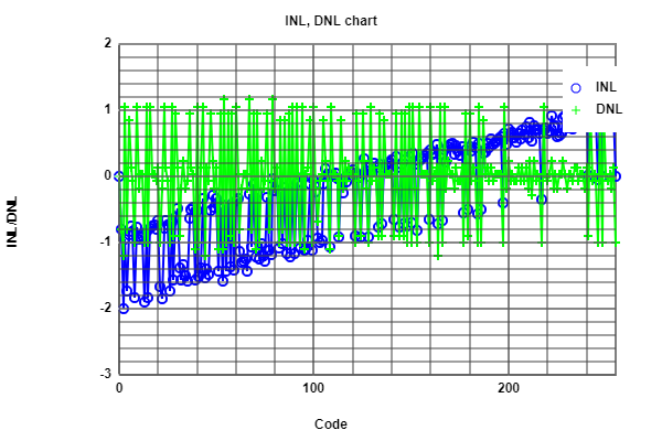
A look at the INL and DNL of the signals show a different result. The graphs are shown bellow. Both graphs contain values far above 0.5. Normally we should loose some bits. Reason again could be the low number of exported points.
INL DNL sine signals 43 periods
INL DNL sine signals one period
Sine measurement of digital calibrated R2R DAC - 419L
Ramp calibration
For the calibration of the DAC a look up table from 0 to 255 is generated. This table is pasted into the signal generator of the webpage. The resulting signal values are loaded into the pattern generator. For the analysis, the rising part of the signal is observated.
Generated ramp signal
This time we used the tools of the oscilloscope webpage. Since we fixed the problem with the low number exported data, we were able to look at the INL and DNL of the whole ramp.
INL and DNL before calibration
The values of the INL and DNL are always between +-0.5. A calibration of the DAC ramp is not necessary. 256 codes accure as planned.
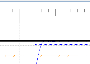
For the calibration, the integer values are extraxted and pasted into the calibration tool. Already during export, the tool shows an decrease of the number of codes from 256 to 195.
INL and DNL after calibration
The figure above shows a big increase of INL and DNL. The calibration made the DAC worse. It is not recommended to use the generated calibration result.
The reason behind the increase of INL and DNL is the algorithm which is behind the calibration. Currenlty it only looks if the value before was higher or not. If so, it takes the same digital outputs as before and one code is lost. In the figure bellow, the green arrows indicate ones the not used code value. Instead of the higher value, the value of the code before is used again.
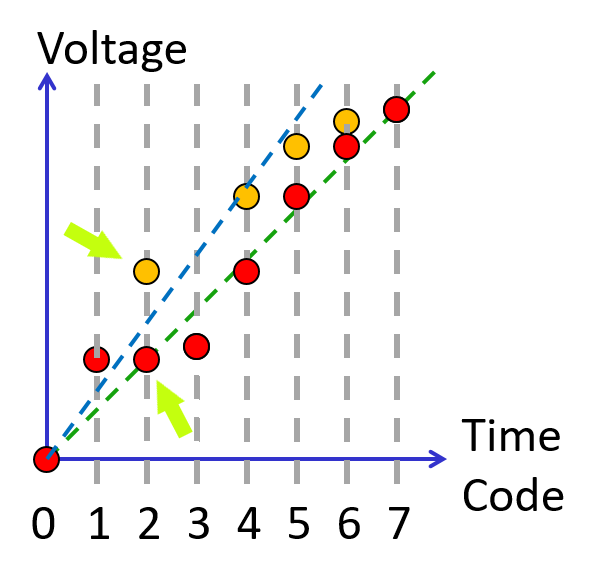
Example for calibration
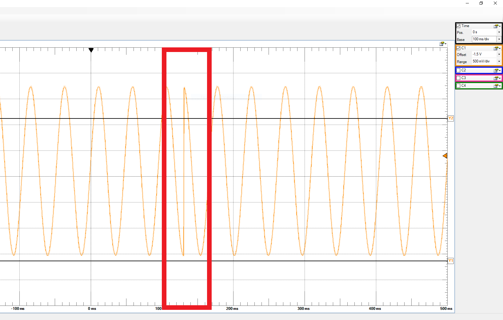
We were not able to finish the calibration of the sine signal due to time issues. We also had problems to figure out our somehow jumping generated sine signal, look figure bellow.
The signal makes a jump in the red marked area. This influences the analysis a lot and has to be fixed.
Generated sine signal problem