Interface Electronics
Web Report Lab04
***936, S
***139, R
|
|
Overview
- Simulation of a 8Bit R2R DAC
- Building a 8Bit DAC on the Digilent Board
- Adapt the simulation to the real measured values
- Analyse INL, DNL and SNR of the simulated DAC
- Measurement of specific settling times of the DAC
- Testing the real DAC with a ramp
- Testing the real DAC with a sine signal
- DAC Calibration
- Compare the simulation with the measurements
- Conclusion
Simulation of a 8Bit R2R DAC
Circuit of the ideal R2R DAC
We created the circuit of an ideal R2R DAC in LTSPICE. Therefore we just used the given structure from the lecture and adapted it to 8 bits.
We do not use any filter at the output.
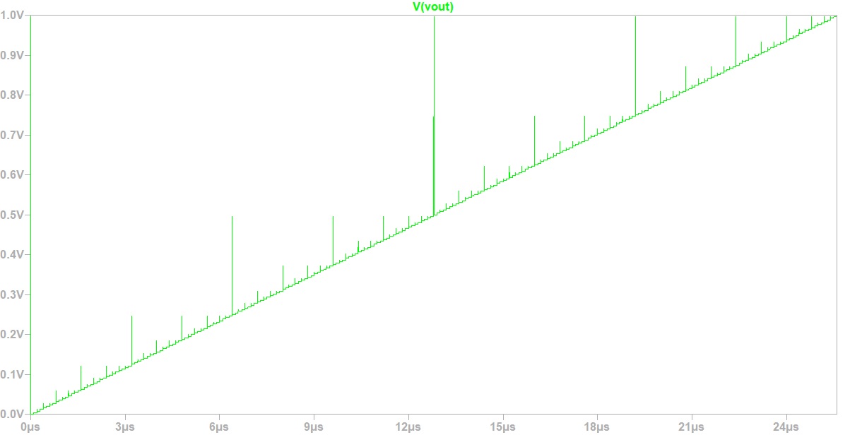
Ramp Simulation of the ideal DAC
For this simulation we used a ramp signal as input for the ADC_DAC_Pipe.
The 8-bit R2R DAC is simulated with the same setup as in Lab 03, which was adapted to a 8-bit measurement setup.
One can see the overshoot with every bit switch. The height of this overshoot depends on, which bit changes.
The change of all bits (127 to 128) creates the biggest overshoot.
The easiest way to smooth these spices is with a RC Lowpass Filter.
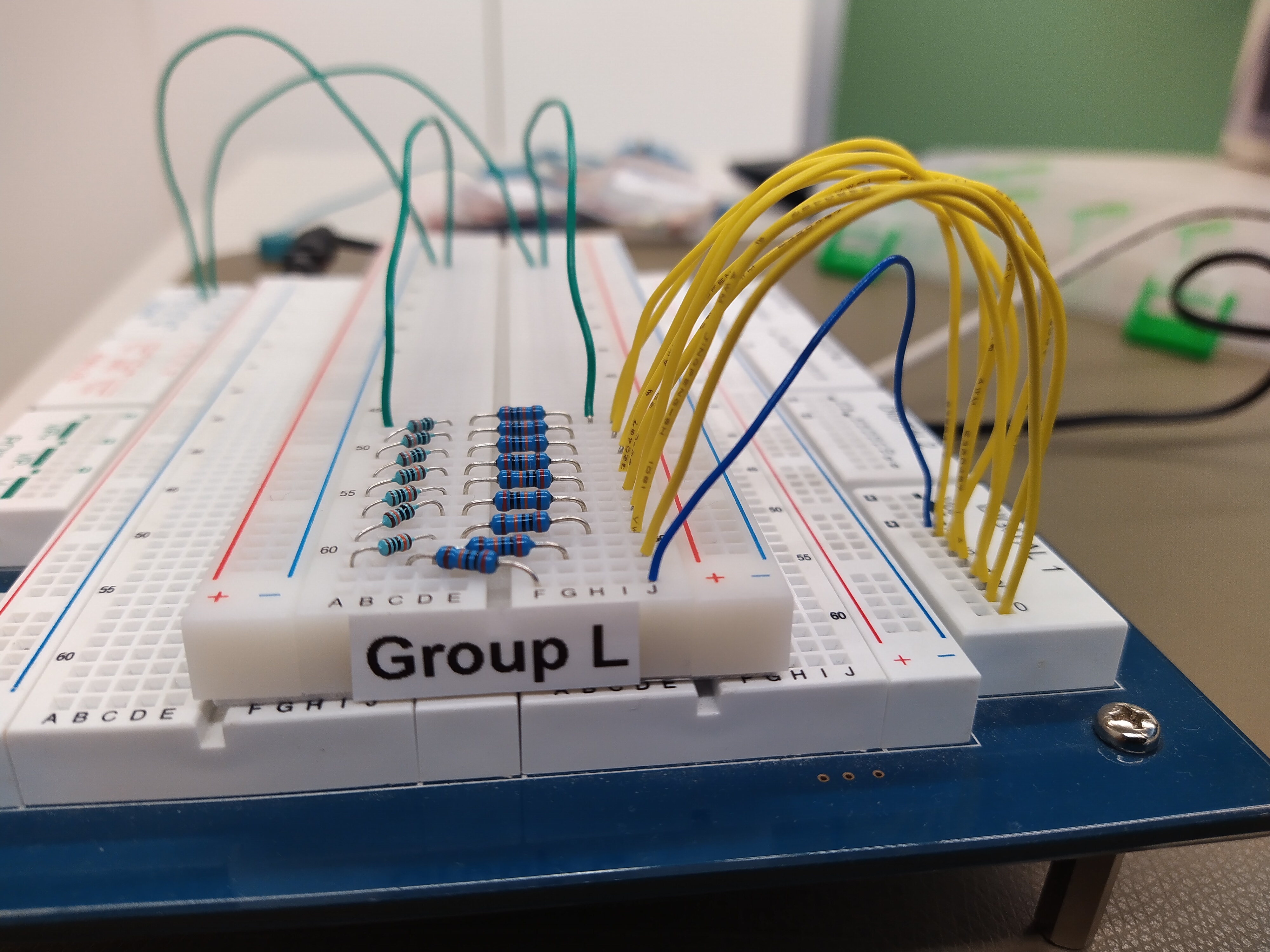
Building a 8Bit DAC on the Digilent Board
Real DAC on the experimental Board
For the realization of the R2R DAC the ideal circuit from the simulation is realized on an experimental board.
The values of the resistances differ from the ideal value. This must be taken into account when simulating the real DAC.
Adapt the simulation to the real measured values
Adapted Simulation to the Real Hardware
As a matter of fact the resistance values have to be adapted to the real values.
The real values of the resistances are measured with a multimeter.
Analyse INL, DNL and SNR of the simulated DAC
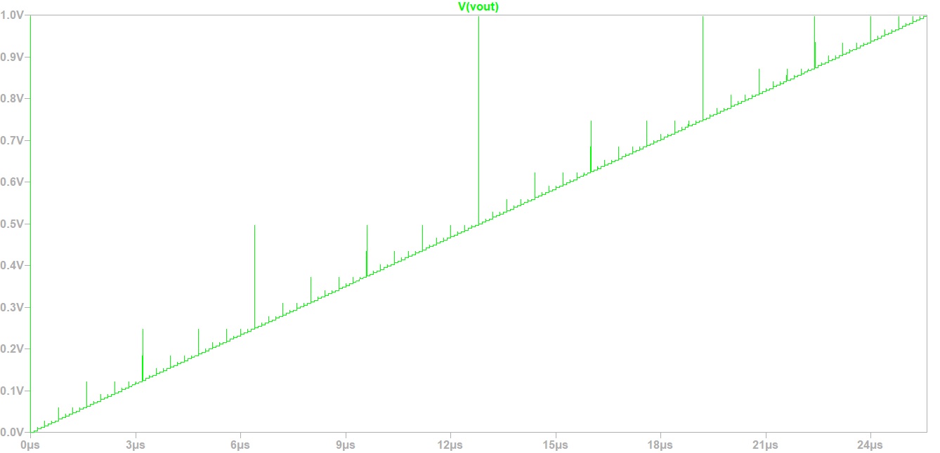
Simulation of the real DAC with a Ramp Signal
The simulation was done using LTSPICE with the same setup and parameters as before for the ideal R2R DAC.
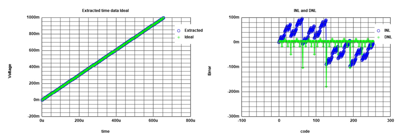
Calculating INL and DNL out of the Ramp Signal
The INL and DNL values of the R2R DAC are calculated by the provided Javascript tool.
The INL and DNL of the simulation is almost ideal. There are only very small values in INL and DNL.
Simulation of the real DAC with a Sine Signal
The simulation of the real DAC with a sine signal as input can be seen in the figure below.
The sine is represented well although one can also see some overshoot during the bit changes.
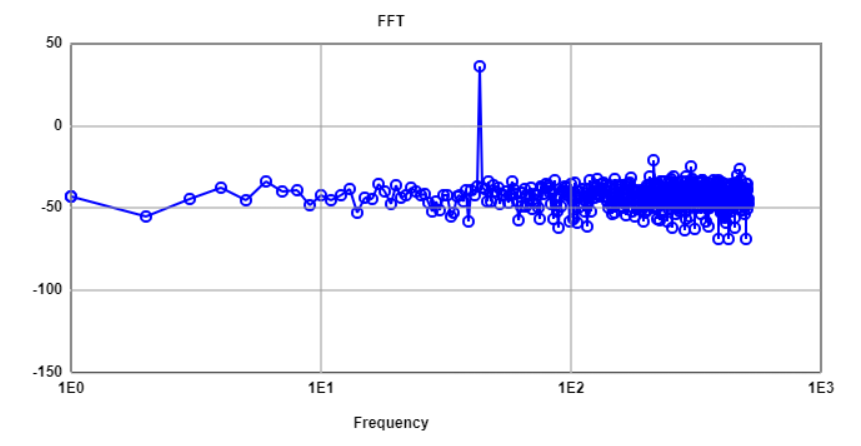
FFT Analysis of the DAC Sine Signal
With the results from the simulation with a sine signal as input, a FFT analysis can be done.
The FFT analysis of the simulated signal can also be done directly in LTSPICE.
The difference to this FFT analysis is, that the Javascript Tool only uses the Calculated Integer Values for the FFT.
Measurement of specific settling times of the DAC
Settling Time between 0 and 255
Now we switched from the simulation to the real hardware.

Test conditions:
- frequency of the signal generator: 10kHz

This test was done with the real hardware. The rise time was directly measured by the experimental board.
The result of the measurement was about 6.5 microseconds.
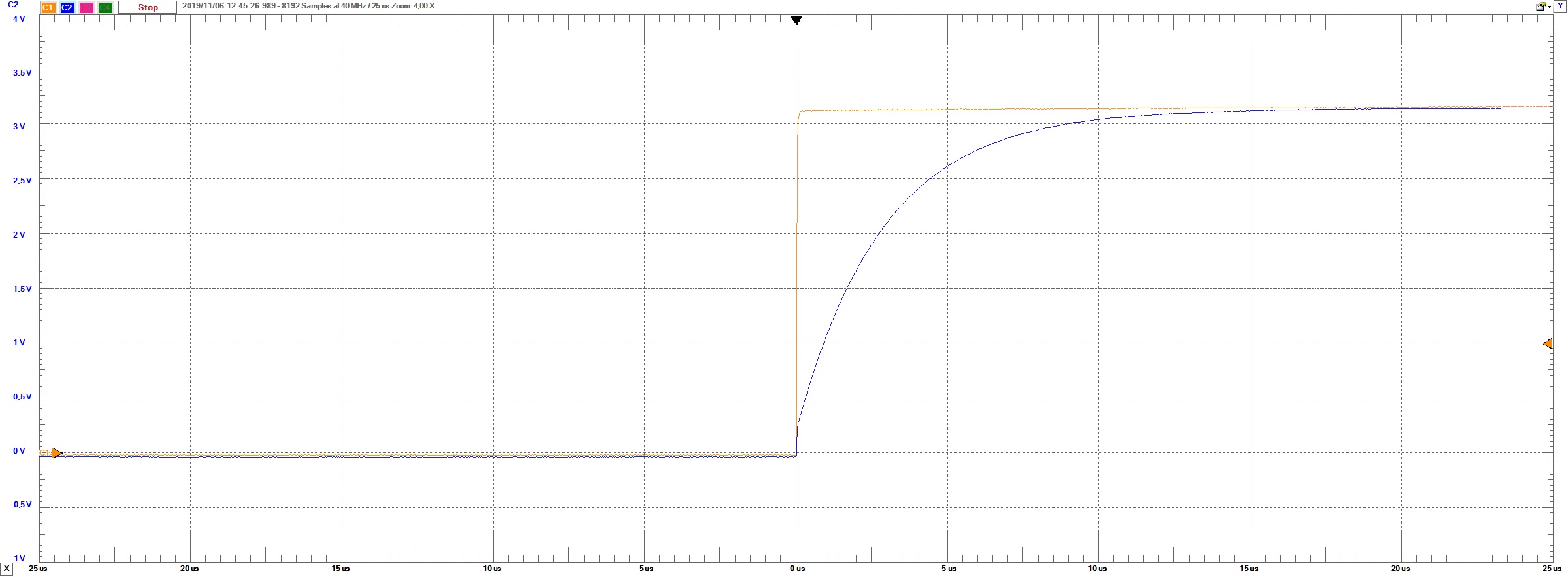
In this test we checked the maximum voltage change of the DAC. This change should have the longest settling time due to the high voltage change.
With this result we could calculate the maximum operating frequency of our DAC.
This is calculated by 1 over the settlling time. The resulting maximum frequency is at about 166 kHz.
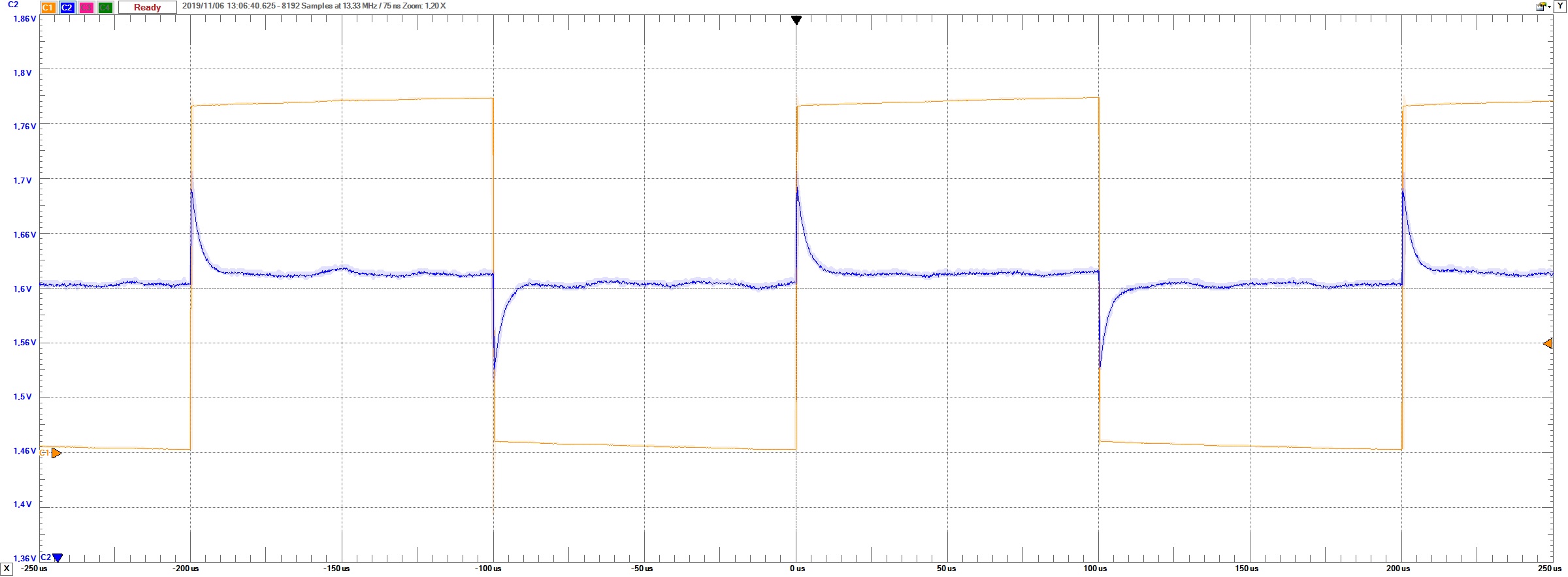
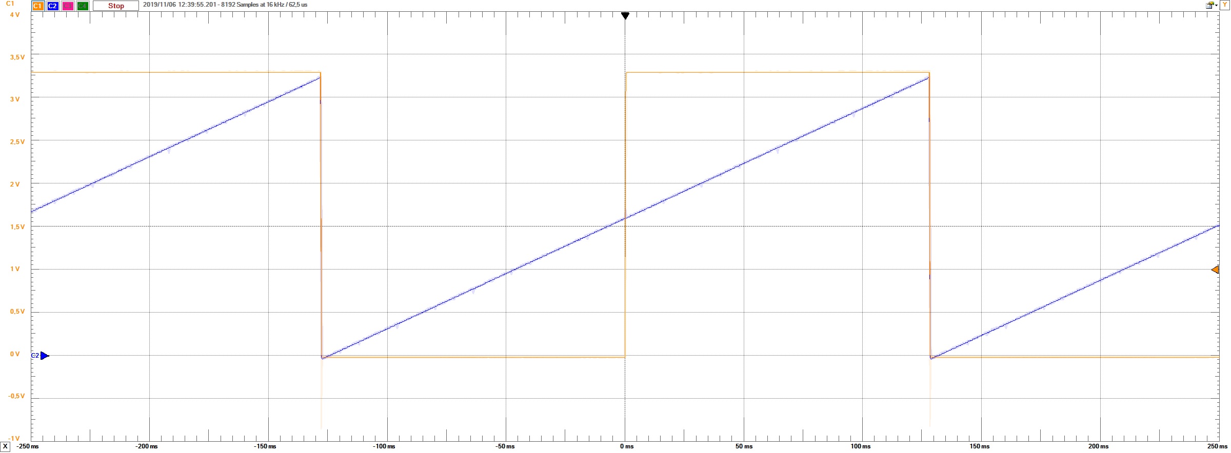
Settling Time between 127 and 128
Test conditions:
- frequency of the signal generator: 10kHz

The picture below shows the bit change from 127 to 128. There you can see the biggest overshoot because of the change of all Bits.
There you can see that our DAC needs the settling time to get the expected output value.
Testing the real DAC with a ramp
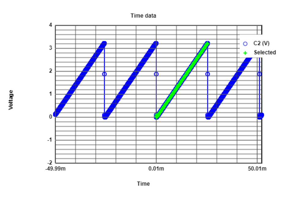
Measuring the real DAC with a ramp signal
Test conditions:
- frequency of the signal generator: 10kHz
- Input: Digital Counter 0 to 255

The time data of the DAC is extracted directly from the oscilloscope. For the analyses the provided Javascript program was used.
To get only one ramp a starting point for the analysis must be defined. We are also averaging the values. 256 values are used due to the length of 8 bits.
Measuring the real DAC with a ramp signal
Test conditions:
- frequency of the signal generator: 10kHz
- Input: Digital Counter 0 to 255
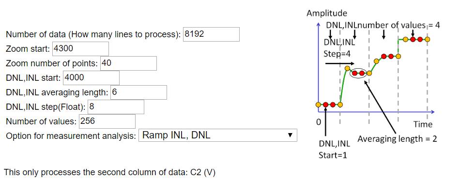
In the following picture one can see the configuration of the analysis tool.
Measuring the real DAC with a ramp signal
Test conditions:
- frequency of the signal generator: 10kHz
- Input: Digital Counter 0 to 255.

Below one can see the INL and DNL values of our DUT. The first values are falling of range because of the settling time of the DAC.
Afterwards the DNL is not bigger than one half of the LSB. This result is better than we expected.
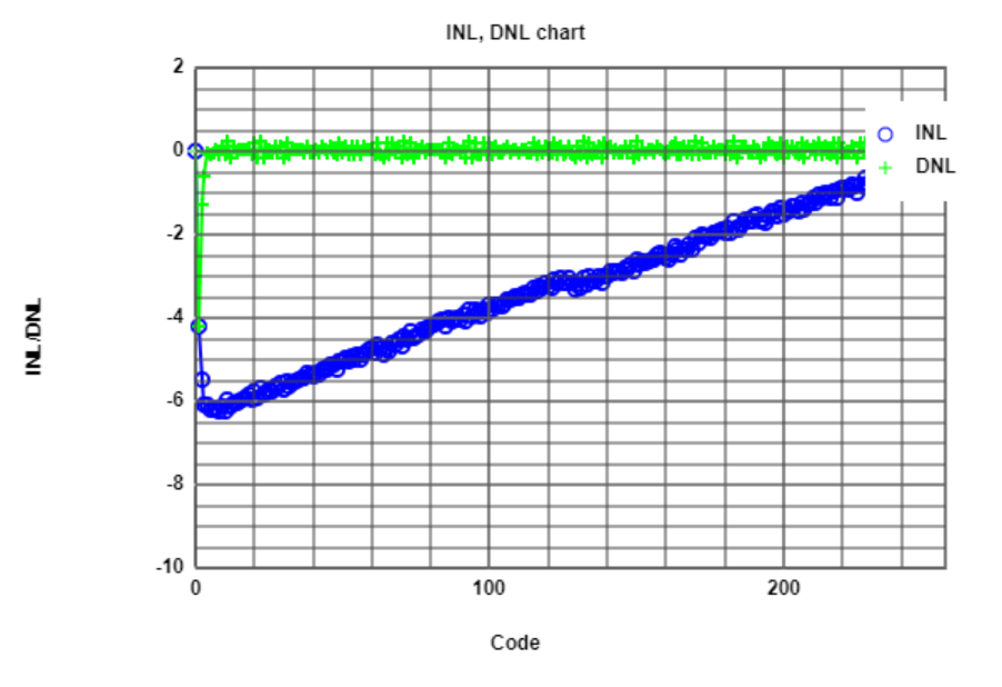
We also tested the ADC with higher frequencys of the Signal generator. Due to the bad settling time of the DAC the signal gets quite worse at higher frequencies.
The output currents of the board are limited and so the system capacity generates a bad settling time.
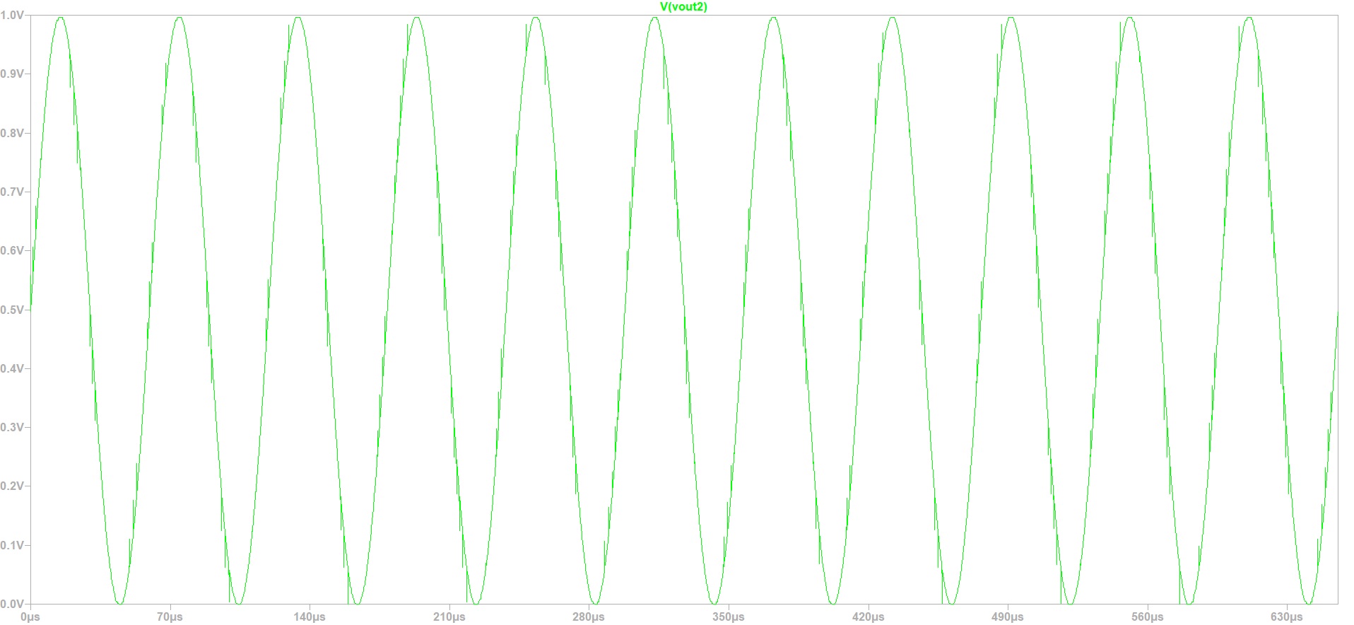
Testing the real DAC with a sine signal
Measuring the real DAC with a sine signal
Test conditions:
- frequency of the signal generator: 10kHz
- Input: 43 Periods sine signal
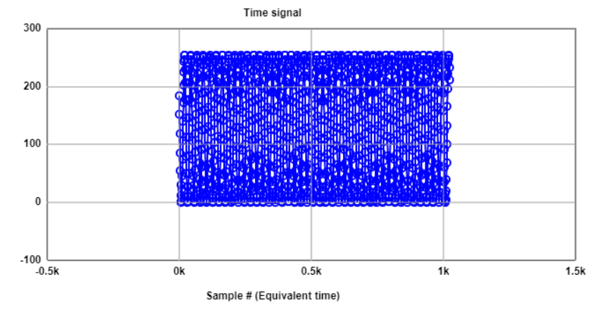
For this test a sine signal was used as input. We used 43 periods to have an odd number of periods.
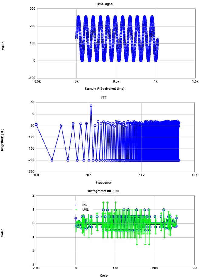
Testing the real DAC with a sine signal
Measuring the real DAC with a sine signal
Test conditions:
- frequency of the signal generator: 10kHz
- Input: 43 Periods sine signal


By use of the provided Javascript tool a FFT analysis can be done. In this FFT one can see the frequency component of our sine signal as the biggest peak.
The normalized value of the frequency is 43. To calculate the real Frequency we must take into account the sampling rate of our averaged values.
We adapted the averaging to the sampling rate of the DAC. Both sampling rates must be the same. We sampled with 10kHz and used 1024 Points for the FFT.
Our Plot contains 512 Frequency Points from F0 to Fs/2. Due to this our calculated Freqency is 419.9 Hz.
Testing the real DAC with a sine signal
Measuring the real DAC with a sine signal
Test conditions:
- frequency of the signal generator: 10kHz
- Input: 43 Periods sine signal


The javascript tool also provides values for SNR. The INL, DNL values can not be used in this because they are not useful for a DAC.
With the ramp signal we verified the DAC and the DAC is nearly ideal. This sine FFT analysis based on statistical methods is more useful for an ADC.
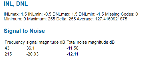
Calculated SNR of the DAC.
Compare the simulation with the measurements
Comparison of simulation and measurement
The best signal to compare the simulation witch the real measurement is the ramp.
Our simulation is done without considering any capacitance.
With a very slow frequency we are able to get nearly the same curve as in the simulation.
The spices are only in the simulation visible, cause capacities in the real hardware are smoothing these spices.
Conclusion
As conclusion I would say that this laboratory was quite a lot of work. In comparison to last semester microelectronics, the provided tools are a lot better explained.
Therefore not so much time is wasted understanding the working principle of the tools. The tests with the experimental board worked well. One problem causes us a lot of time searching the problem.
The export of the oscilloscope function has not the right format. So we spend a lot of time searching for the right configuration of the output.
Later on we just replaced the "," by "." with notepad. Alternativ is the american standart for export. Her the "," must be replaced by a ";".