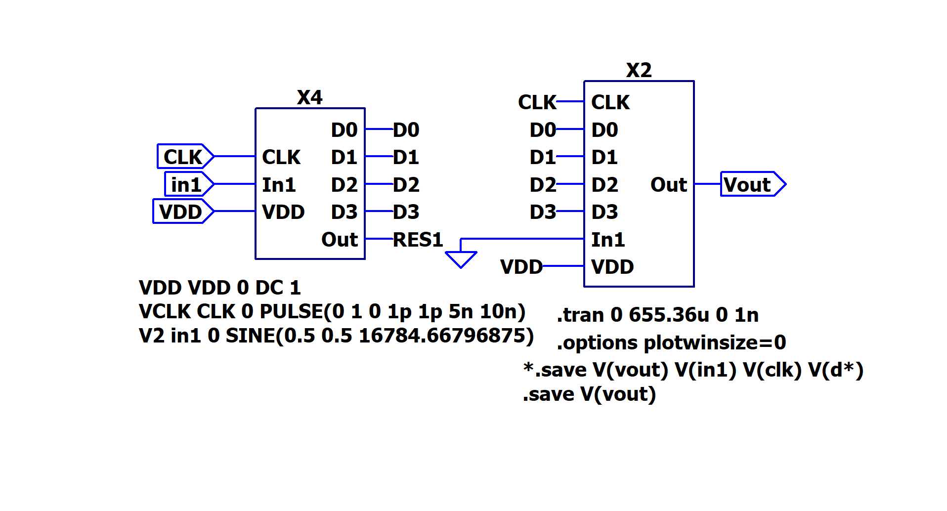
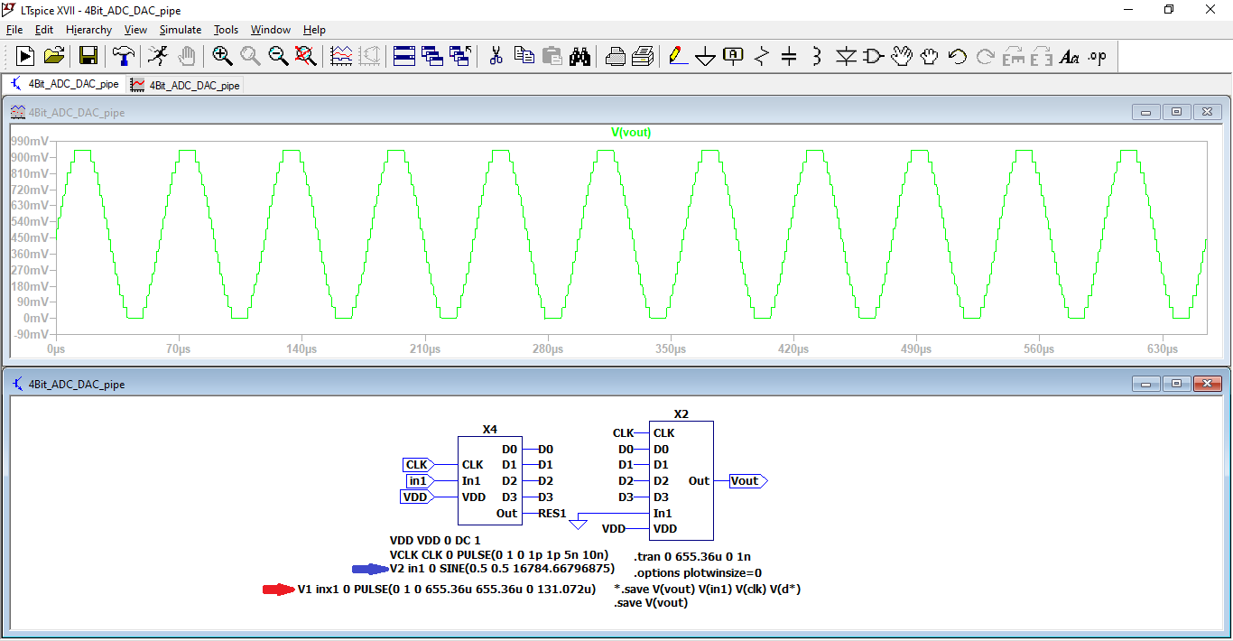
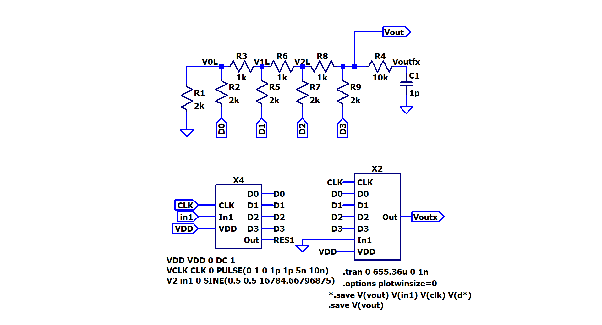
ADC DAC schematic
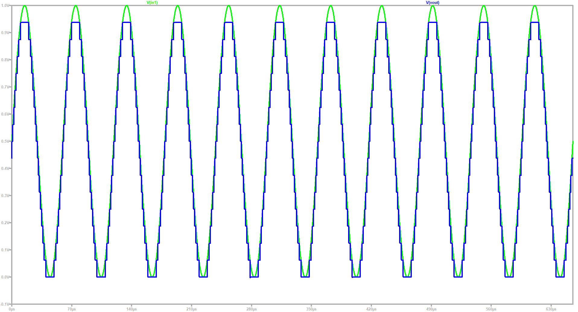
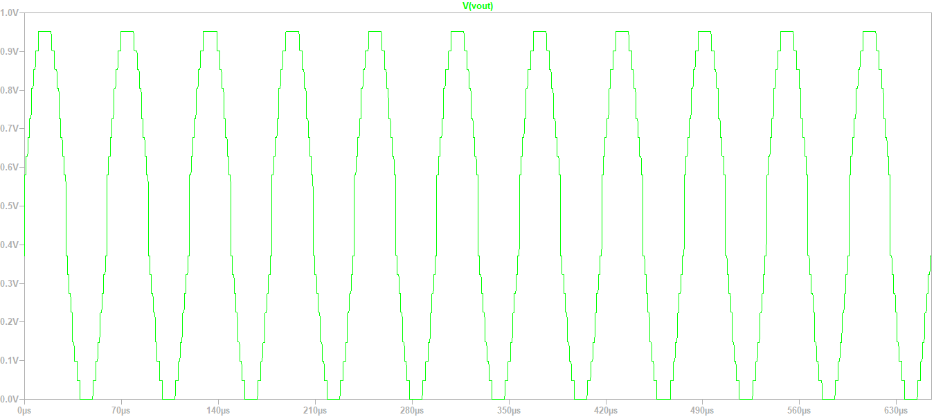
4-bit ADC and DAC are drafted on the software LTspice as shown in the figure.The AC block shall convert an analoge sine signal into digital which the DAC converts into analoge, as shown by simulation in the graphic next to the circuit.
 |
 |
FFT Simulation
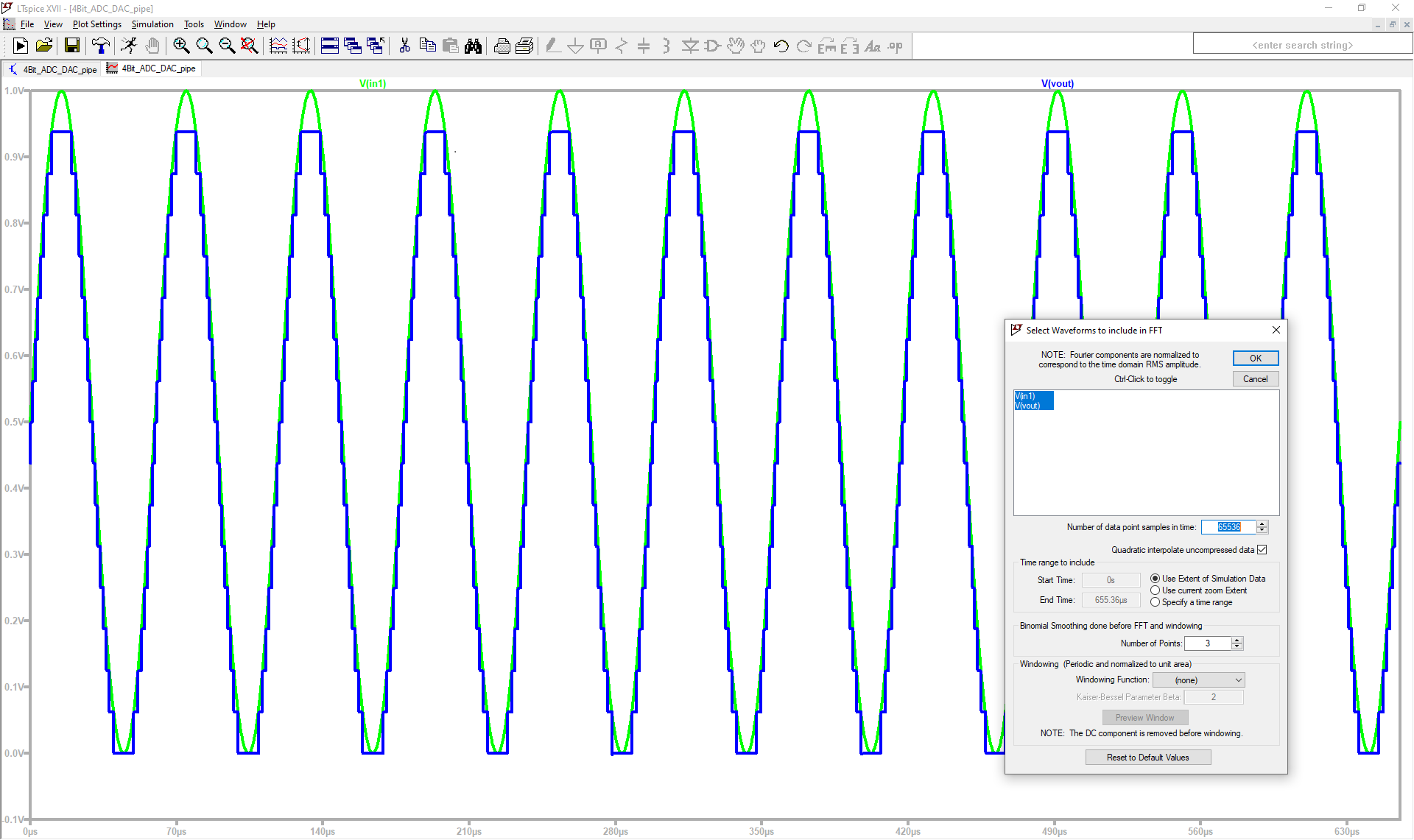
It is possible to run a FFT in LTSPICE. Having plotted the last graph, we click on View/FFT on the GUI.A window appears to choose the number of values for the FFT. We set it to 65536.
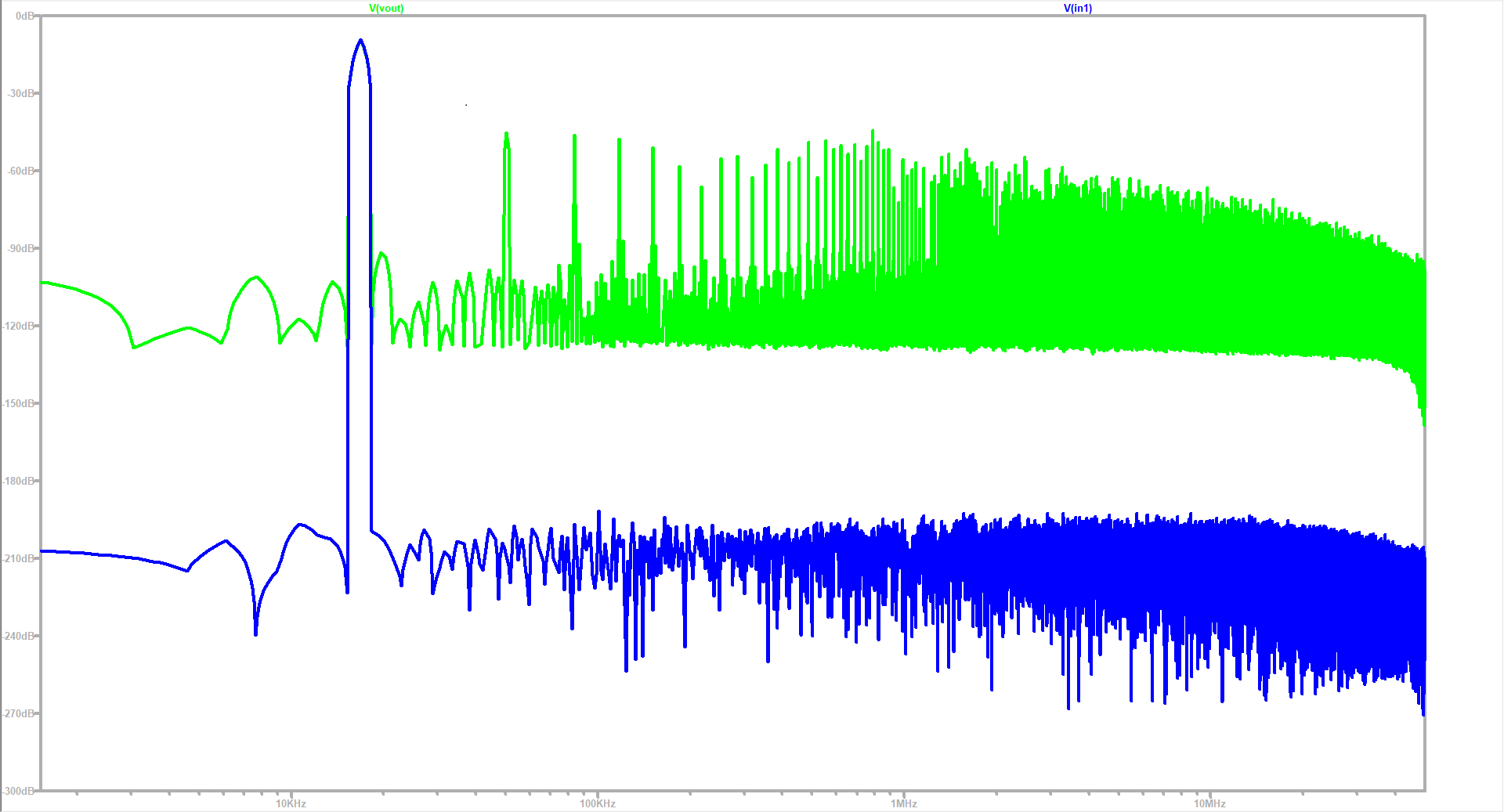
Finally a graphical representation of the SNR is obtained.
 |
 |
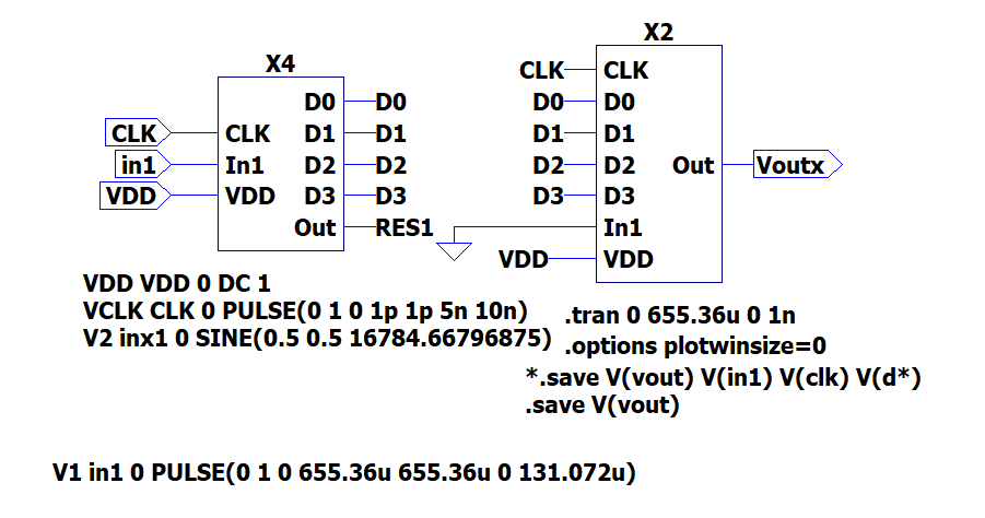
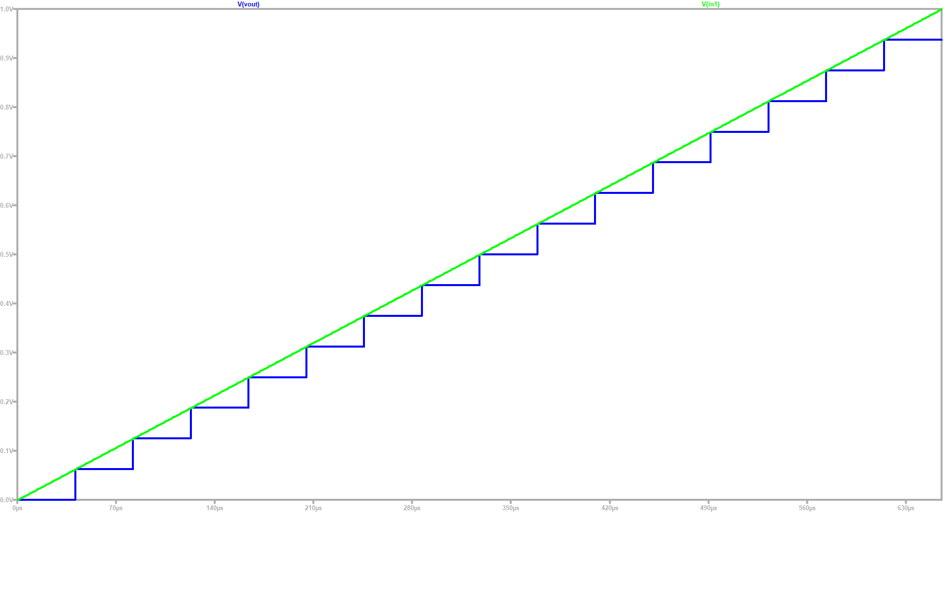
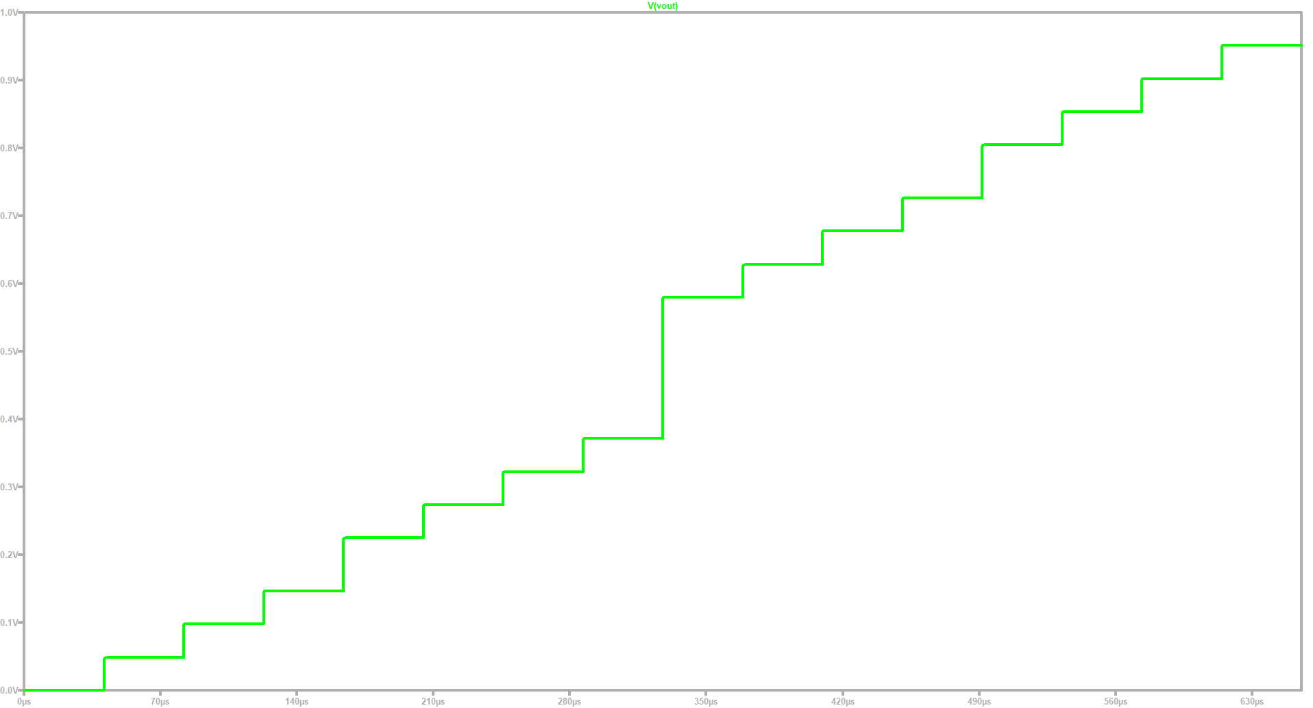
Ramp test
For our ramp test, we need to create a new pulse input voltage and to disable the sine input voltage by naming it by another tag.This input must have its parameters as specified by the directive "V1 in1 0 PULSE", with 665.36us for rise and fall time, which corresponds to the simulation time.
The simulation gives as result an equally distribuited step graph along the ramp.
 |
 |
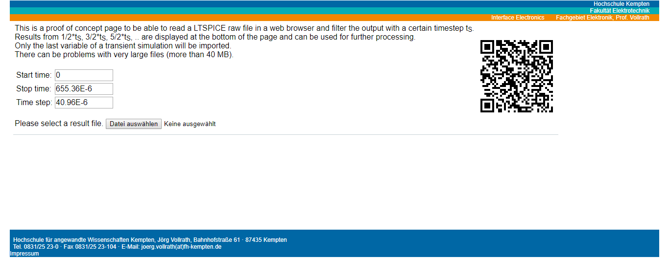
Further analysis
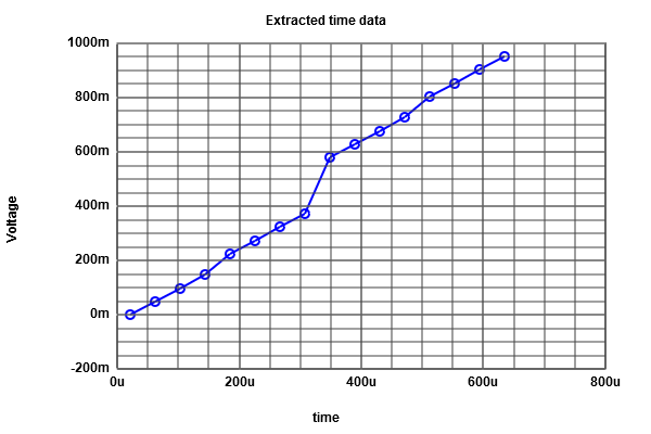
LTSPICE generates data from the last simulation into a .RAW file in the same directory as the schematic file.Through a Javascript program in the personal page of Prof. Vollrath we can upload the .RAW file in order to obtain curves of the converters.
Here is necessary to state start and stop time. These must be the indicated by the transient directive.
For the time step we divide the simulation time by the number of steps in the last resulting curve, which were 16.
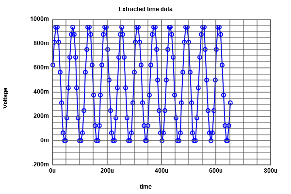
Further analysis
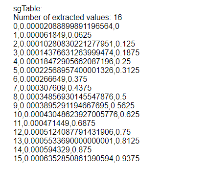
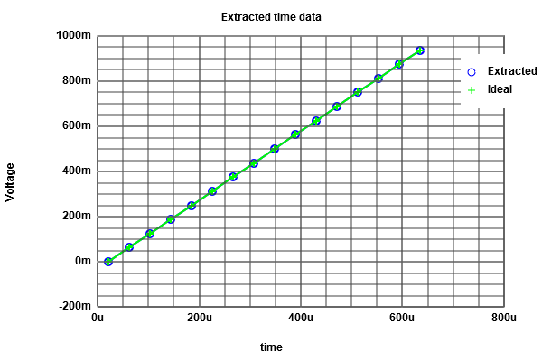
Having processed the values with the tool it can be seen a graph of the extracted values, as well as a table of it.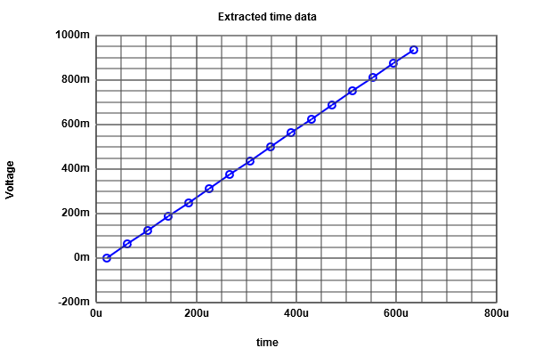 |
 |
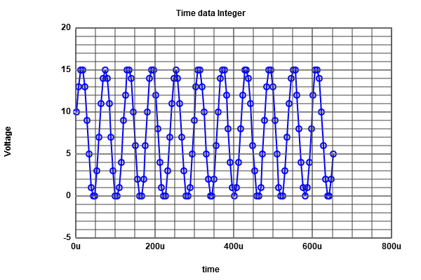
Further analysis
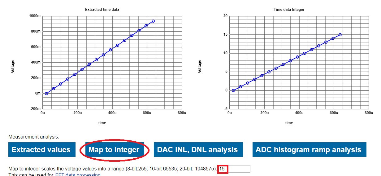
A new graph can be generated from the first by mapping it from a given scale.For that, the desired range is introduced in the indicated box. In our case we want 0-15.
We click then on map to integer to get the graph.
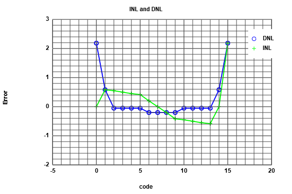
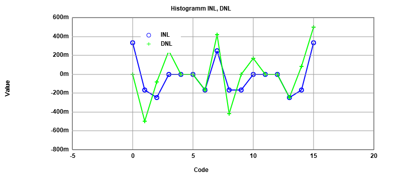
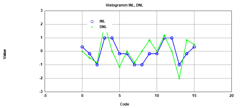
INL and DNL analysis
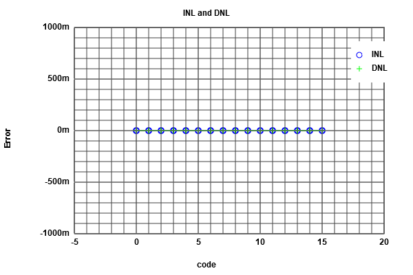
We can also compute the INL and DNL values and display their curves.Now we click on "DAC INL, DNL analysis" button to see results.
As expected, there is no error in any of the intervals.
 |
 |
ADC histogram test
Changing the time step to 5.12us means more samples to take.Doing this causes errors as shown below.
.png) |
.png) |
ADC histogram test
Mapping again by the same range 0-15 and clicking on the "ADC histogram ramp analysis" yields the following.Because of the time step, it is taken 8 samples for each iteration of the mapping range, making the scaled curve look like a step.
For the INL and DNL there is no error.
|
.png) |
Sine output analysis
The same analysis done for the ramp signal can be made for the firstly sine signal in the simulation.To do so, the original sine voltage source must be enabled again and disabled the pulse source.
A simulation is run in order to get the needed data into the .RAW file.
Sine output analysis
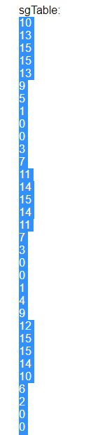
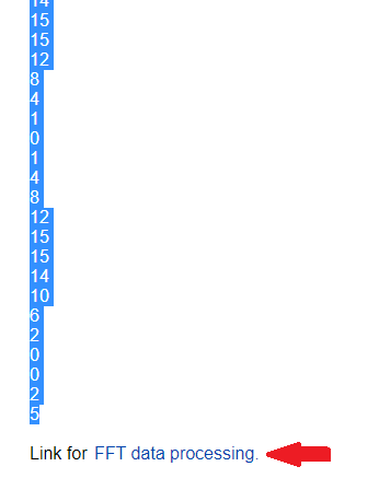
By using the previous values for start and stop time, time step and map to integer, the RAW file is uploaded.The tool takes 128 samples throughout the period, making up 16 values from top to bottom of the sine wave.
The sine output is then scaled into the specified range.
 |
 |
ADC histogram test on sine wave form
Plotting the the DNL and INL values by the "ADC histogram ramp analysis" function does not give us the correct curves, given that the calculation is made by using an average constant.For this case, by copying the values table that is calculated with the tool "Map to integer" it is possible to solve this issue by using another tool by following the link of FFT data processing as indicated at the end of the scaled values table.
 |
 |
 |
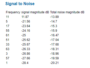
FFT Javascript tool
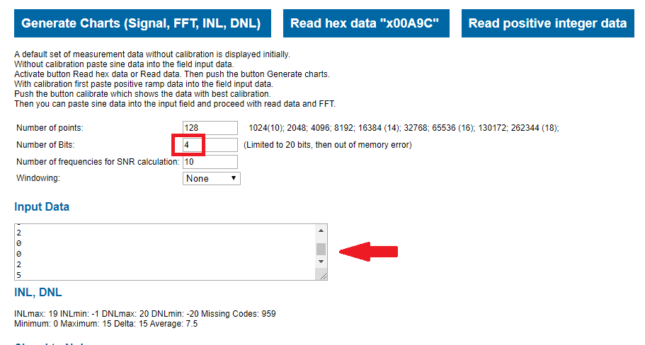
This section of the personal page of prof. Vollrath can make FFT analysis of sine functions.First, the copied values must be pasted in the "Input data" box. The "number of bit" box value has to contain 4, which correspond to our the number bits of the converters.
Clicking on the "Read positive integer data" and "Generate Charts" buttons processes the given data.
FFT Javascript tool
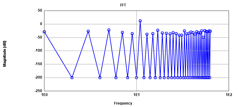
A FFT curve is generated after having processed the values; a lack values can be seen on it and some noise level.Aditionally, a true INL and DNL is obtained and a Signal to Noise table is computed as shown below.
 |
 |
 |
R2R DAC analysis
A new R2R DAC circuit is incorporated.This replaces the first DAC.
Running a simulation shows the same behavior just like the last one.
Altering the R2R DAC
If we change resistor values of the R2R DAC, it will malfunction as shown graphically.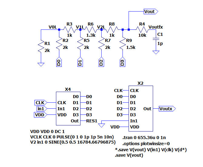 |
 |
Tests on new circuit(signal output)
The same procedures made previously with the Javascript tool are once again done with the new data.Important ot see is the INL DNL histogram as it shows clearly errors
Tests on new circuit(ramp output)
Now we are enabling again the pulse input on the schematic. The plot after simulation has some big steps among them.Utilizing the RAW data and setting a time step of 40.96us on the Javascript tool yields the next results.
The new DAC makes their most pronounced erros arround the middle of the simulation as can be seen.
 |
 |
bad r2r.png) |
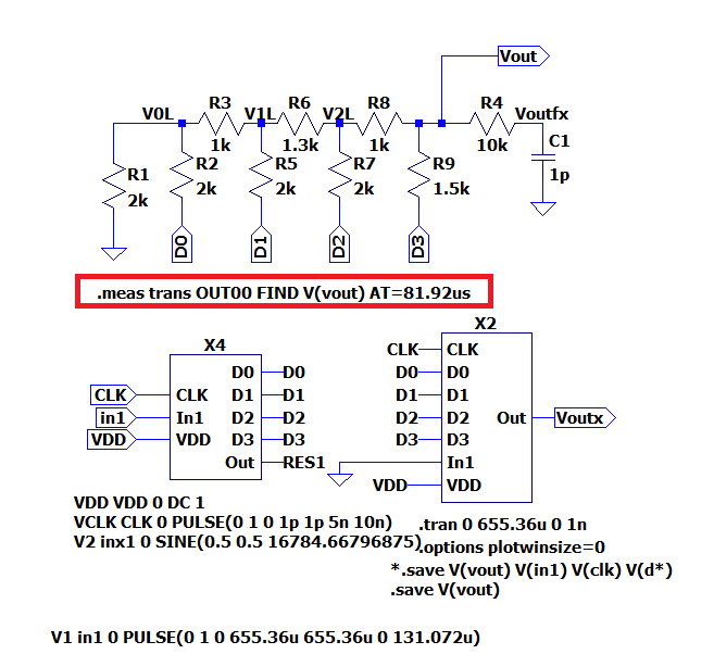
Extracting data through LTSPICE
LTSPICE offers a way to measure certain values at a specified time during a simulationFollowing a syntax format as indicated below we decide to measure the output at the time of 81.92us
Once the simulation is complete, the captured value can be located on the GNU tab View/SPICE Error Log.
 |