Interface Electronics
Laboratory 04: Simulating and measuring an R2R DAC
Group M
***640, R
|
|
Overview
- Motivation
- Building an 8-bit R2D DAC
- Ramp test from simulation data
- Sine test from simulation data
- Testing the breadboard R2R DAC
- Ramp measurement set up
- Settling times
- INL and DNL analysis for ramp signal
- Sine signal test
- INL, DNL and FFT for sine signal
- DAC digital calibration
- ADC digital calibration
- Comments on the lab exercise
- Conclusion
Motivation
In this laboratory an 8-bit R2R DAC will be tested in simulation as well as in practice for ramp and sine signals for the purpose to compare both ways and evaluate
performance.
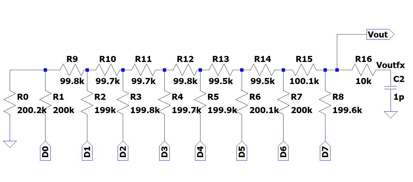
Building an 8-bit R2D DAC
With resistors of 100k and 200k Ohms it is built on a breadboard a R2R DAC. This very circuit is drawn on LTSPICE by taking a 4-bit R2R DAC and expanding it into 8-bit
with the resistor values taken by multimeter.
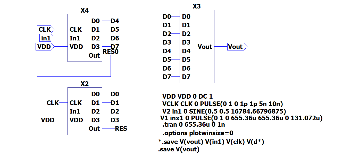
A previously made 12-bit ADC DAC LTSPICE circuit is modified in order to make it 8-bit and to raplace the DAC with our R2R DAC as shown below, being this the one
tagged as X3.
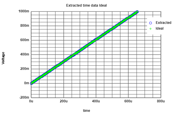
Ramp test from simulation data
As we can see for the DAC, analysing the data after a simulation on LTSPICE shows an almost perfect ramp compared with the ideal.
The INL and DNL result with error due to the imperfection of the resistors.
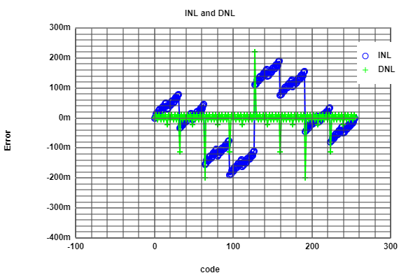
Sine test from simulation data
Computing INL and DNL gives a pretty constant values along few points that greatly exceed the recommended LSB margin.
 |
 |
Testing the breadboard R2R DAC
With the purpose to test the DAC performance, we connect it to a a device called Electronic Explorer. The DAC digital inputs are connected to this device its MSB and output
to measure. This electronic board is linked by USB to a PC and by means of a software, Waveforms, we are able to generate and measure signals.
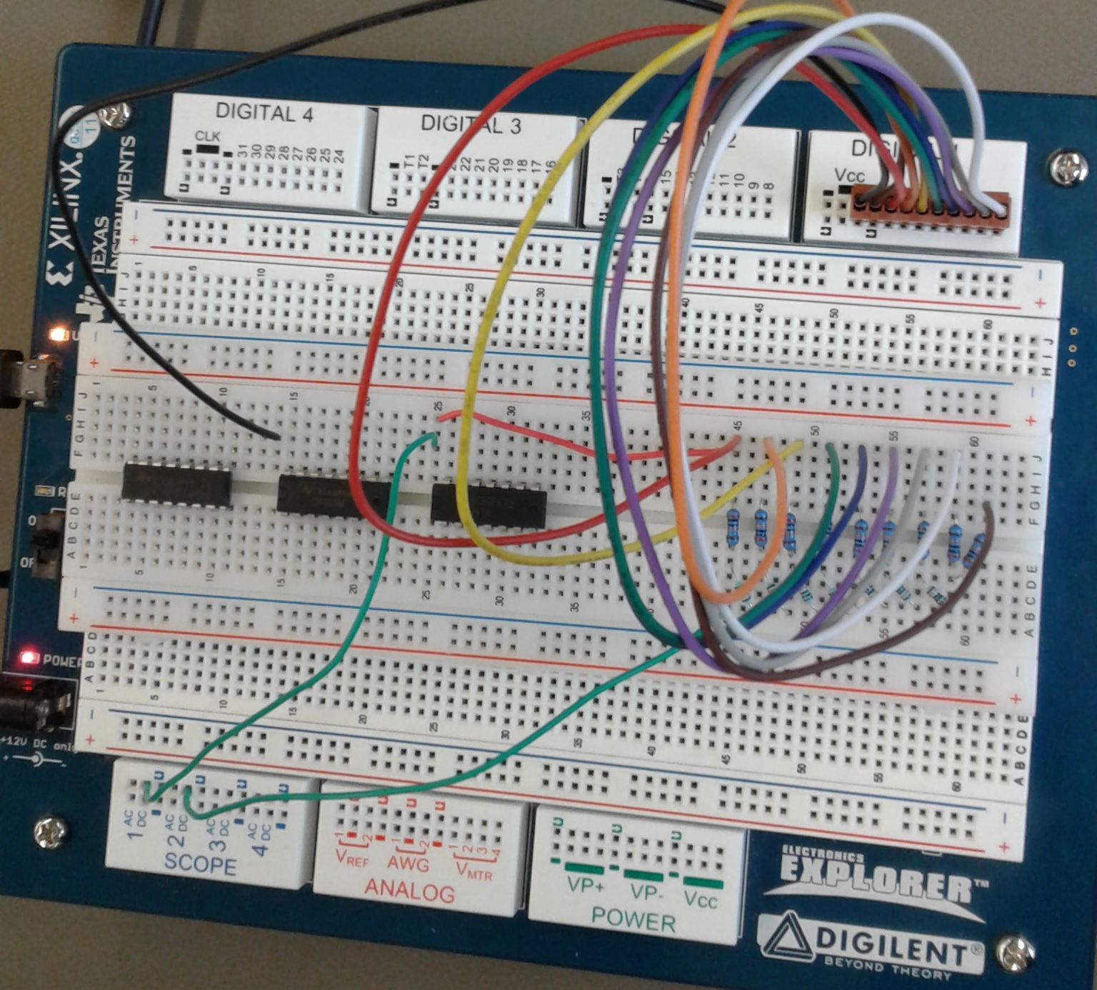 |
Ramp measurement set up
A ramp test for our DAC can be made by creating a 8-bit bus for the input and setting a binary pattern. The output measurement can be seen on the oscilloscope
of this software.
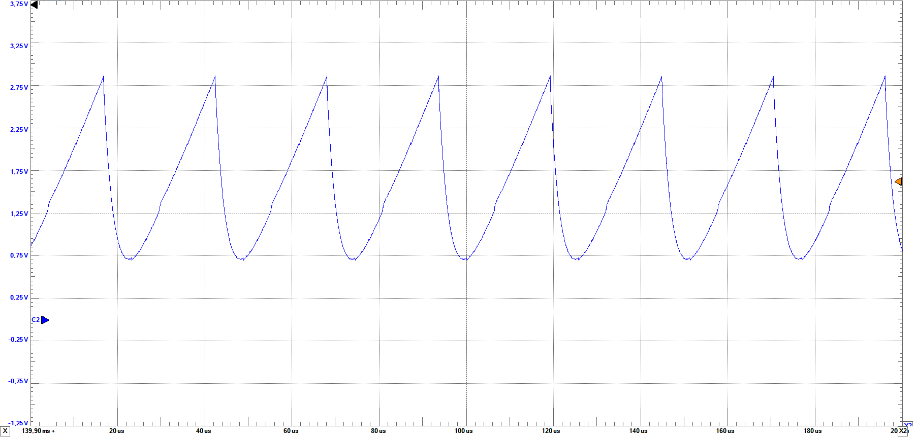
The output C2, which correspond to the DAC output, shows a sawtooth waveform. Setting the input frequency at 10MHz, 1MHz, 100kHz, 10kHz, the waveform gets sharper the
lower the frequency is. Varying the frequency at lower rates we obtain a very good graph at 1kHz.
Figures showing DAC output at diferent frequencies.Left 10MHz, center 100kHz, right 1kHz.
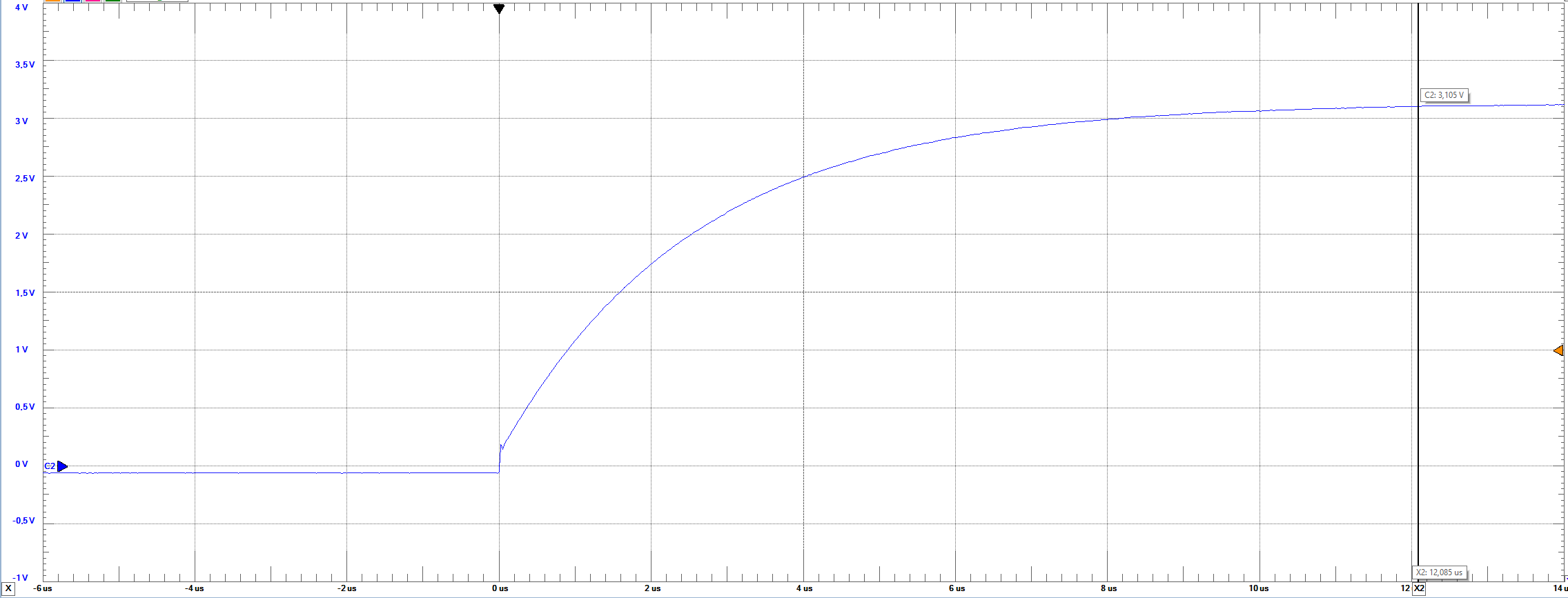
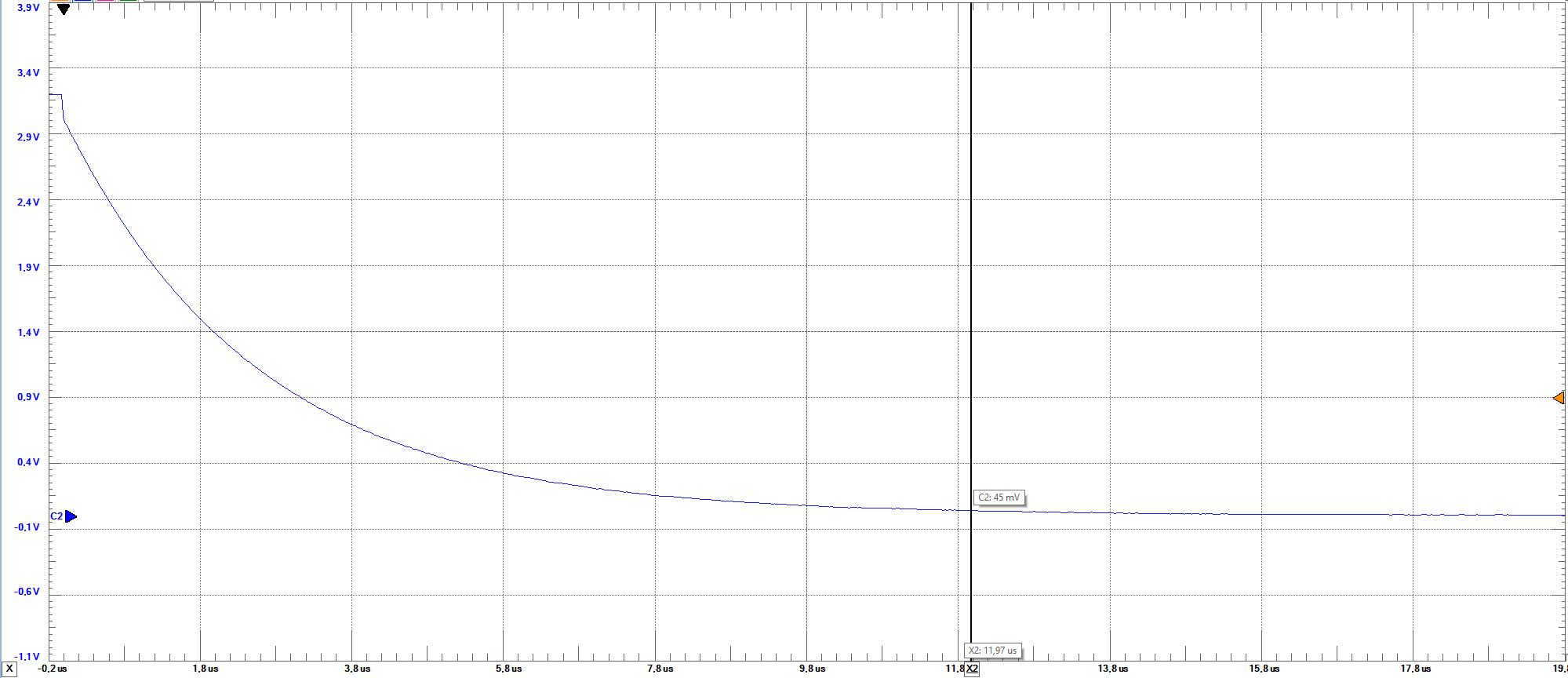
Settlings times
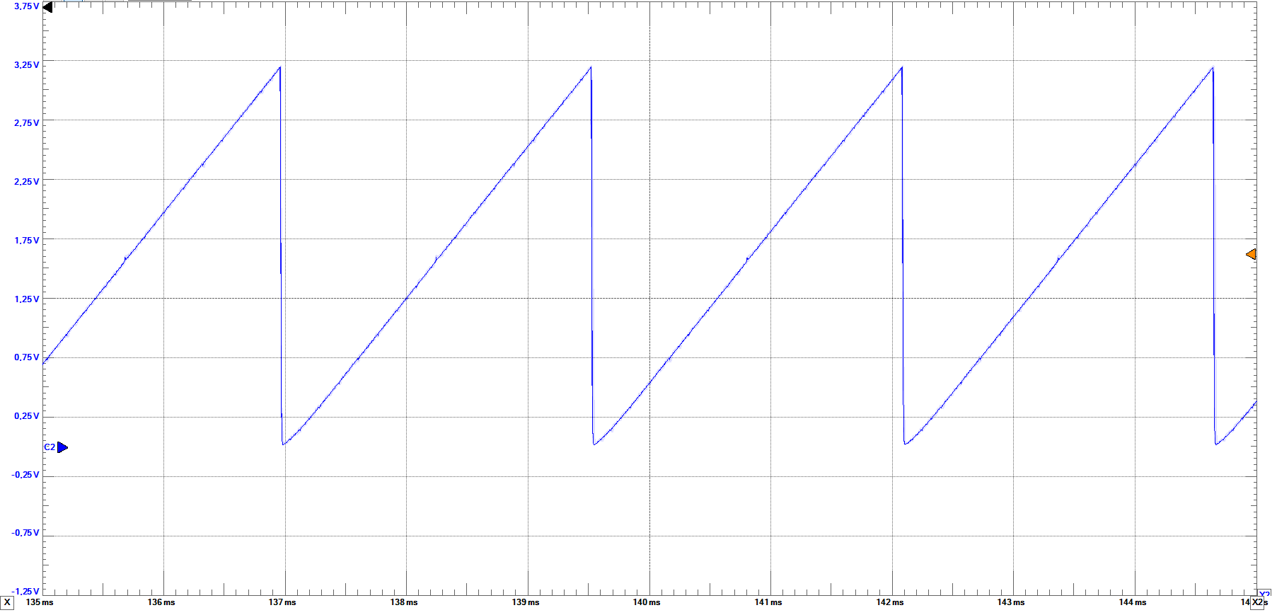
Waveforms gives us the possibility to measure the rising and falling settling times of the DAC when it reaches a step.
For that we change to clock for the bus on the patterns window for middle and full scale. By varying the frequency we find out that at higher frequencies
the step takes longer time to reach and also the time it stays on the step is shorter. At 1kHz we obtain the shortest settling times and
most stable step as displayed.
From left to right rising and falling full scale settling times at 1KHz: rising time=12.085us; falling time=17.82us
|
 |
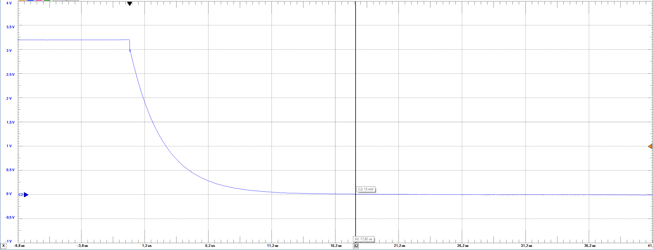 |
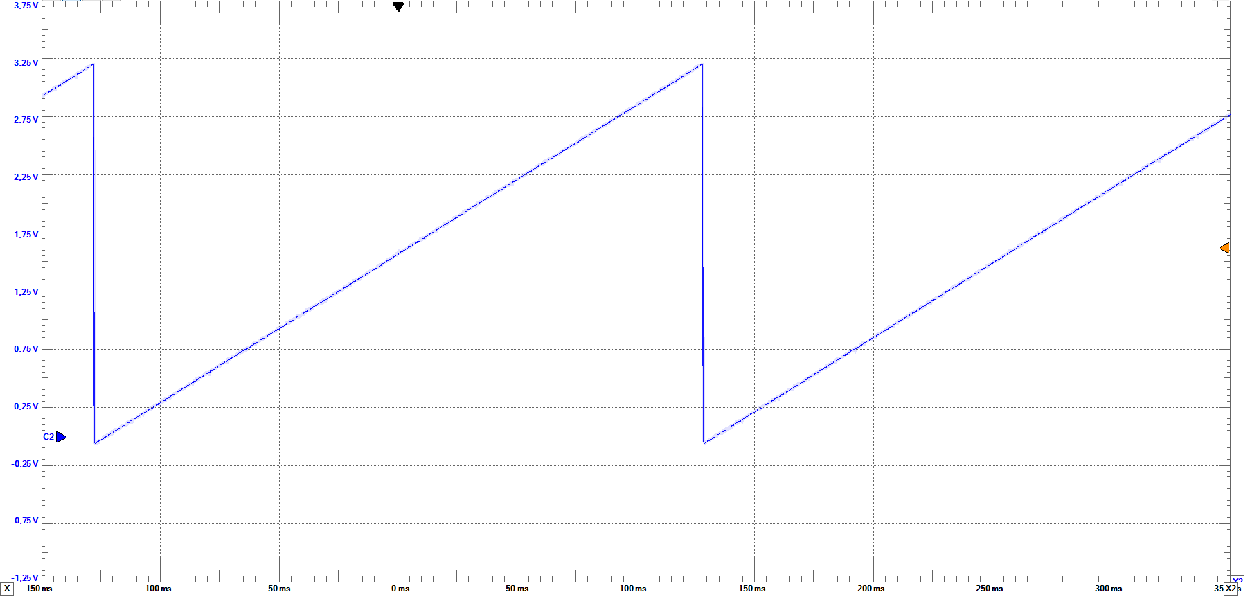
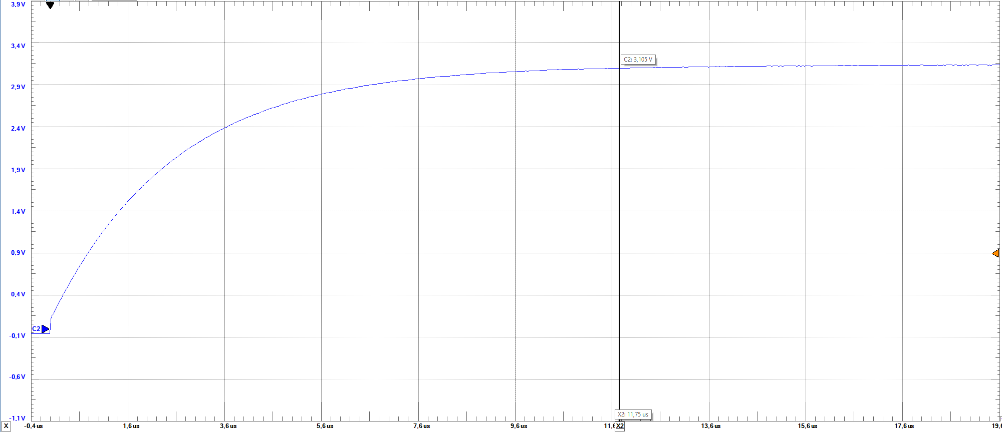
Settlings times
Measurements at middle level are practically the same as at full level as illustrated on the figures.
From left to right rising and falling mid scale settling times at 1KHz: rising time=11.75us; falling time=17.92us
|
 |
 |
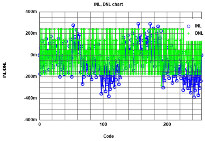
INL and DNL analysis for ramp signal
It is possible to extract values of the plot generated by the software and processes it to analyze a ramp. To do so, on the Scope we click on export and
copy all data showed. With the help of the Javascript App ReadOsci on the page of Prof. Vollrath this data can be computed to get the INL and DNL of one ramp.
However, the data extracted from Scope provide data for more than one ramp. To overcome this issue, only points that correspond to one ramp are selected.
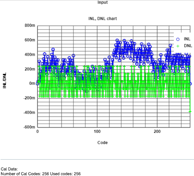
INL and DNL analysis for ramp signal
Having computed the ramp data, it is given the next results at 1KHz, the most suitable frequency in the experiment. As can be seen, for error margin it presents
more than acceptable values for INL and DNL. Judging by these results, there is no need to change resistors.
Sine signal test
We now proceed testing the converter with two 8-bit sine signals as an input, being one of 1 period and the other of 43 periods. In order for the patern generator to
create these signals, files containing the binary information of the periods are created from the course internet page. The type of pattern is changed to
custom on the pattern generator window and then a file is uploaded.
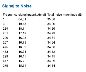
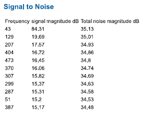
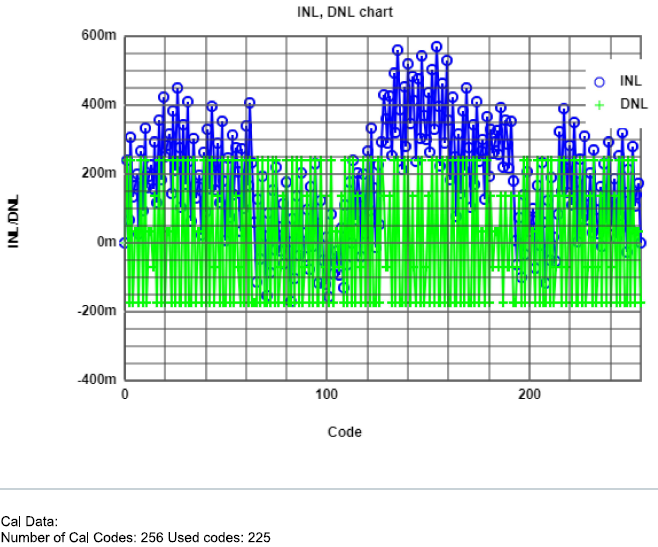
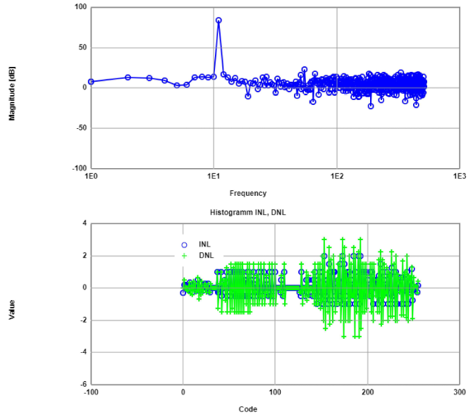
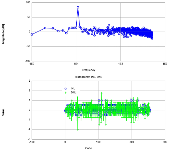
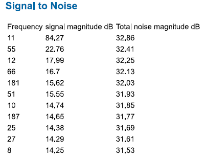
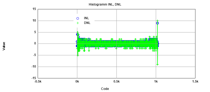
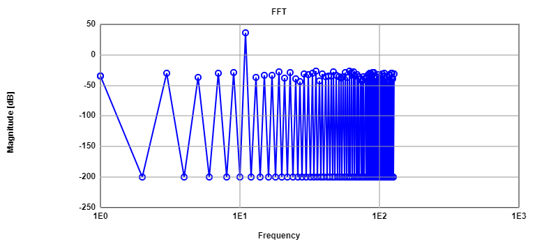
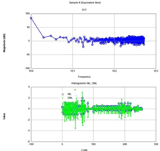
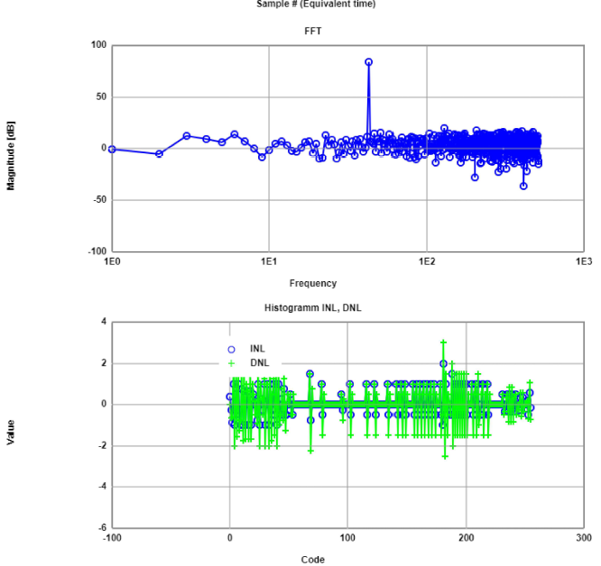
INL, DNL and FFT for sine signal
In order to take data properly from the oscilloscope for sine analysis , it is necessary to get displayed the number on the oscilloscope the number of
periods of the input signal. Using the exported data from the oscilloscope, the next step would be to obtain integer values of the sine curve with the help
of the Javascript App Read oscilloscope data. These values are then processed in the FFT App, where INL, DNL FFT are computed.
|
Results from FFT analysis for sine 1 period(left) and 43 periods(right) signal from samples at 2 KHz. Both FFTs present no harmonics. Regarding INL and DNL the 1 period signal
is better,but both exceed ±0.5 LSB on many codes.
|
 |
 |
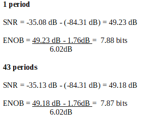
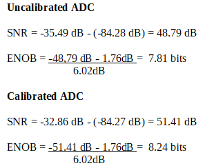
INL, DNL and FFT for sine signal
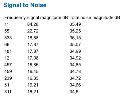
This App also give us signal to noise values. With this we are able to calculate the Effective number of bits at the respective periods. It is seen that both
ENOBs are minimal different and are just llittle less than 8 bits.