1. ADC DAC setup
2. Simulation and analysis of a ramp signal: DNL, INL, LSB
3. Simulation and analysis of a sine signal: FFT, DNL, INL, SNR
Operation
The goal of labaratory exercise 3 was to build ADC(analog to digital converter)connected to a DAC (digital to analog converter) electrical circuit using the LTspisce program.
This electrical circuit was used to simulate ramp and sinusoidal signals in circuits with different parameters. ADC and DAC data converter concept is starting base for
doing simulations and analysis of a ramp signal (DNL, INL, lSB) and sine signal (FFT, DNL, INL, SNR).
Step 1
|
|
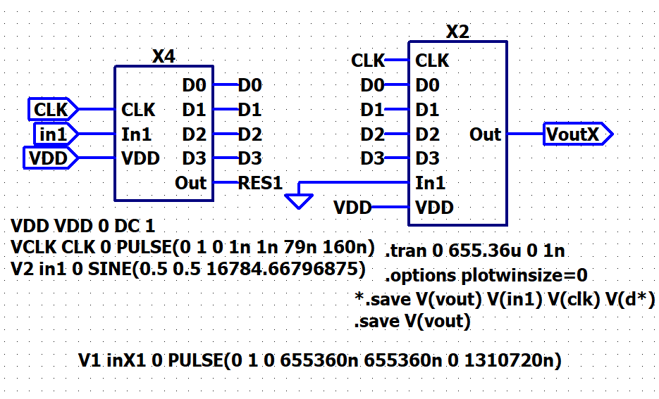
4 bit ADC and DAC converter was built with in LTSPICE program. Simulations with given schematics were conducted.
Simulation checks, that ADC and DAC inputs and outputs of the converters were showing ideal parameters.
Test for FFT to calculate signal to noise levels was held.
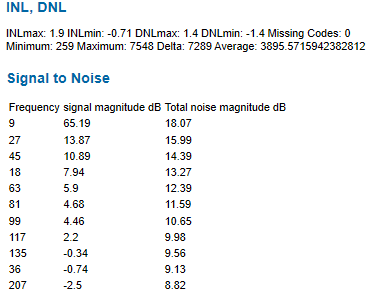
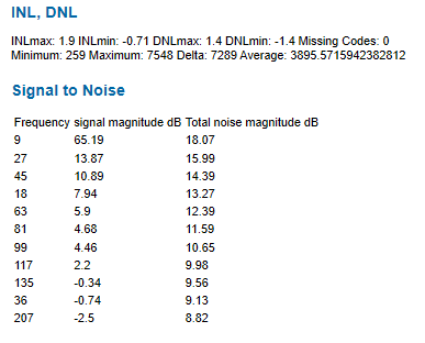
INL and DNL were obtained and those parametes were zero and hence could be said to be ideal converter case.
|
|
Step 2
|
|
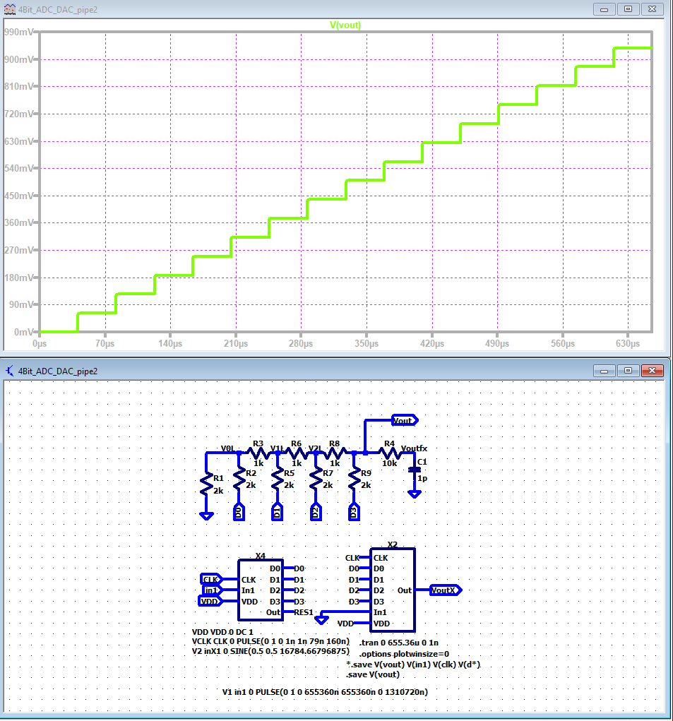
Then 4-bit DAC converter was replaced with 4 bit R2R DAC converter and same ramp and sine input signals were given inorder to analyse the INL and DNL parameters using FFT.
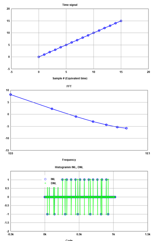
FIrst the ramp signal was analysed. From the ramp shaped transferer curve,DAC output was observed as a voltage reading(Picture 2).
DAC INL and DNL analysis (filtering of the signal) using java script tool (FFT) were performed. Then The INL and DNL graphs were obtained (Picture 3).
|
|
Step 3
|
|
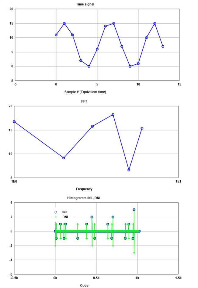
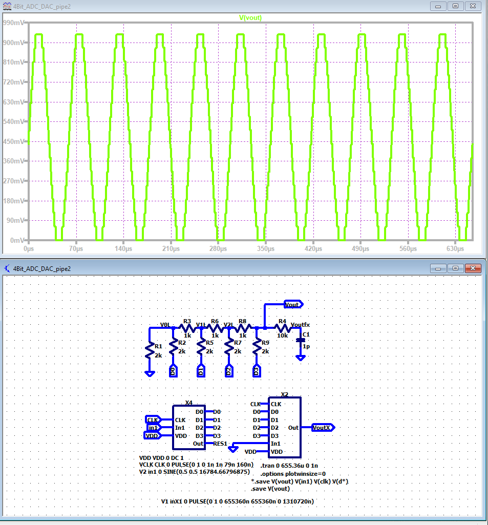
Then sine signal was given as the Input(Picture 6). FFT analysis was done to observe the INL and DNL parameters (picture7)
|
|
Step 4
|
|
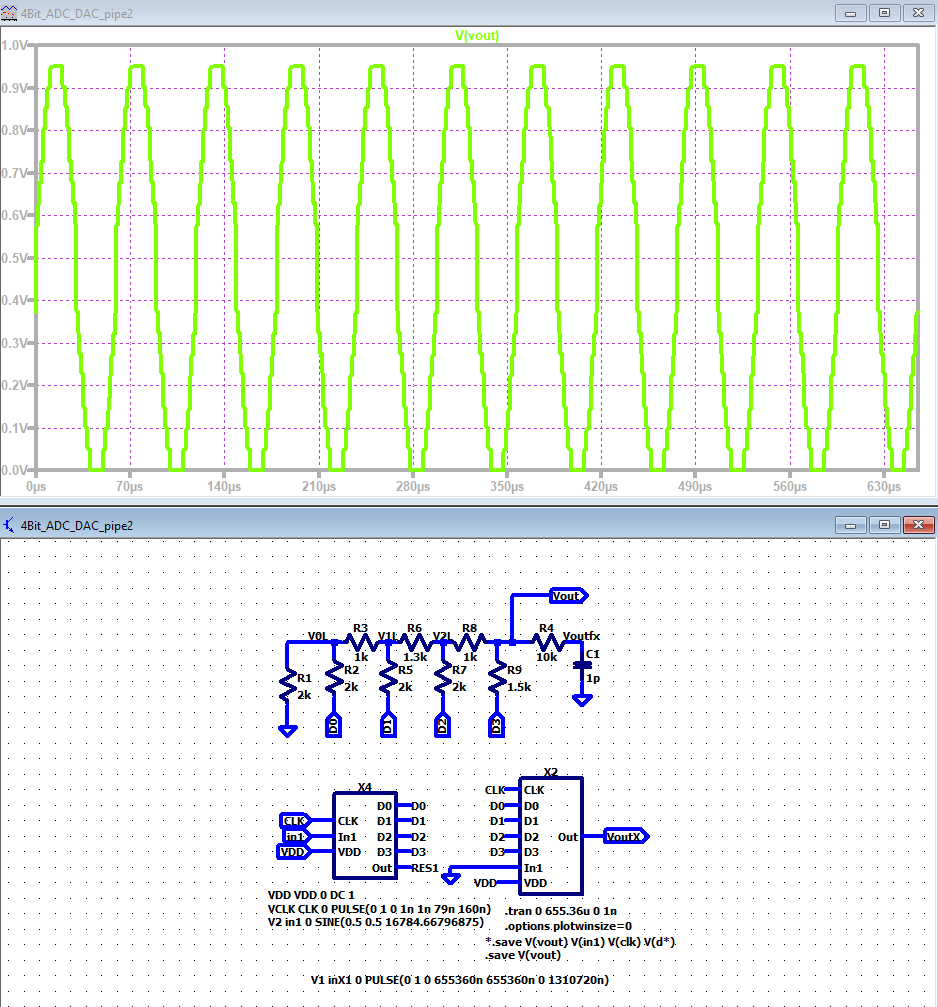
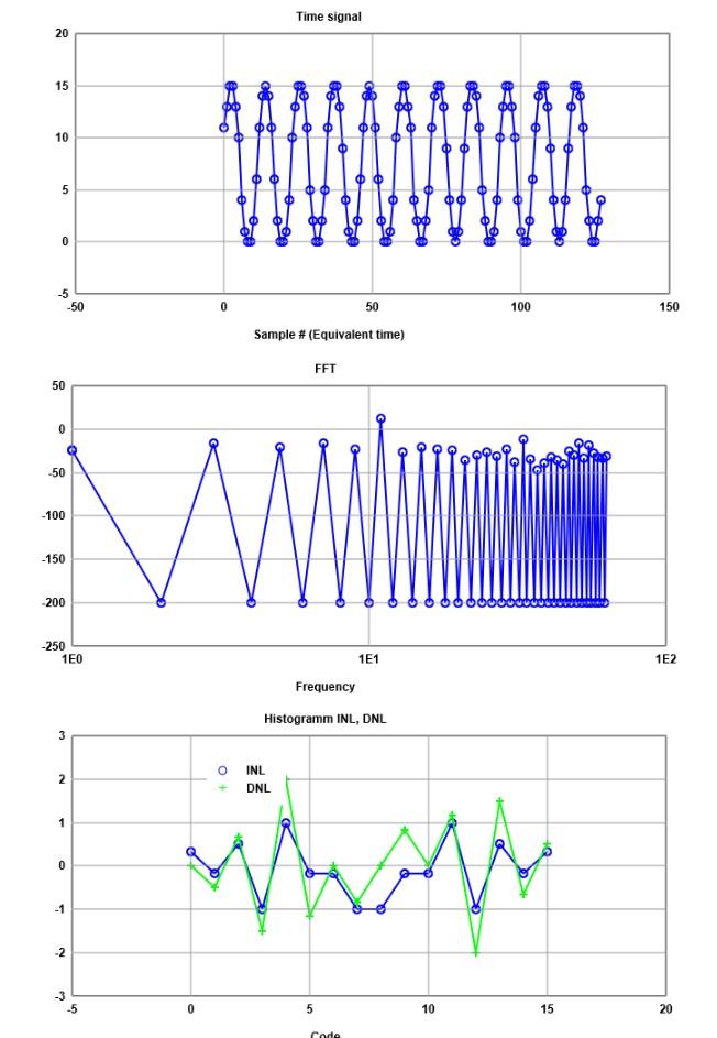
As the above experiments were done under optimum parameters, no error could be seen. Therefore some resistor values of 4 bit R2R DAC were changed to implement some error.(picture 9)
Then same FFT test was done in order to observe the INL and DNL results (picture 10)
Big jump in the center.
|
Picture 9
s
First chart on the picture 10 is time-domain. On the second graph we can see FFT response and through that we can see the fundamental frquency, harmonics and noise seperatly.
Last chart shows us that some values form the ILN and DLN lines are beyond +1 and -1. These values are accounted as the signal errors.
|
|
|
|
Conclusion
We have observed the behaviour of 4 bit ADC and DAC converter when a ramp and sine signal are input. In optimum or ideal conditions INL and DNL values were observed to be zero and can be deduced that there were no error in conversion. Once the DAC parameters were changed, it was observed that the INL and DNL values obtained beyond +1 and -1 which can be concluded due to the non optimisation of the DAC parameters.
|