1. R2R DAC
2. Resistance measurement and LTSPICE schematic
3. LTSPICE simulation: Ramp
4. INL, DNL extraction
5. LTSPICE simulation: sine
5. FFT, INL, DNL, SNR
Operation
The goal of labaratory exercise was to analyse the INL and DNL values of the constructed 8 bit
R2R DAC by inserting Ramp and Sine Inputs to the circuitry. For implementation of this exercise
the circuitry had to be constructed. For this, the resistors with approximate values of 1k and 2k were
used. After the real circuitry buildup on breadboard had been finished, the model of the circuitry
was created in LTSPICE. Ramp and sine tests were simulated in the program and FFT, INL, DNL
were calculated using webpage "ADC measurement FFT analysis" provided by professor. Values
of FFT, INL, DNL and SNR were documented and analysed. For circuitry analysis the ramp and sine
waveform were generated using the "DDS" web page provided by proffessor. Settling times for R2R
DAC were measured.
|
|
R2R DAC LTSPICE Simulation
|
|
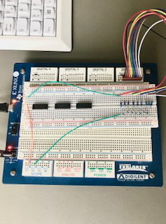
8 Bit R2R DAC was built on the bread board and resistor values were measured.
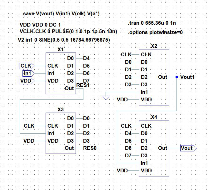
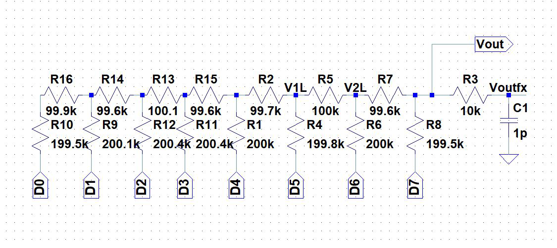
A 8-bit R2R DAC was built in LTSPICE with the measured resistance values.
Ramp and sine were simulated and extracted from INL, DNL and SNR data.
Ramp test was simulated.
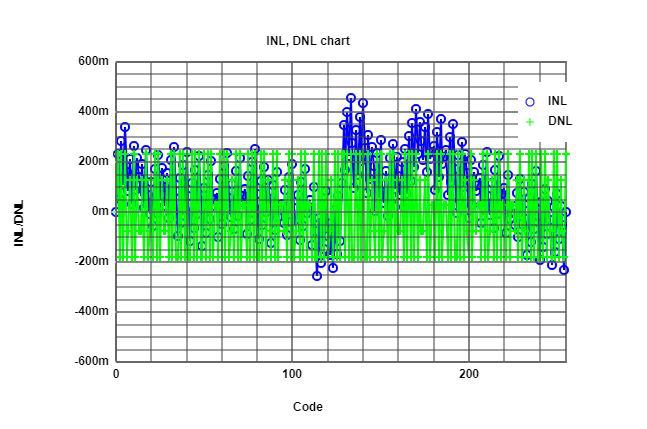
INL, DNL were calculated as follows:
Extracted values from LTSPICE were calulated with the help of the "FFT webpage":
The obtained results of INL and DNL did not exeed +/- 0.5, which states that no
bits were lost.
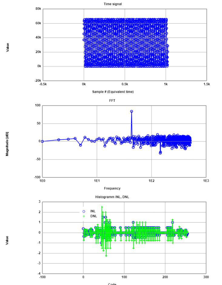
sine signal test was simulated
INL, DNL were calculated as follows:
Extracted values from LTSPICE were calulated with the help of the "FFT webpage":
The obtained results of INL and DNL did not exeed +/- 0.5, which states that no
bits were lost.
|
|
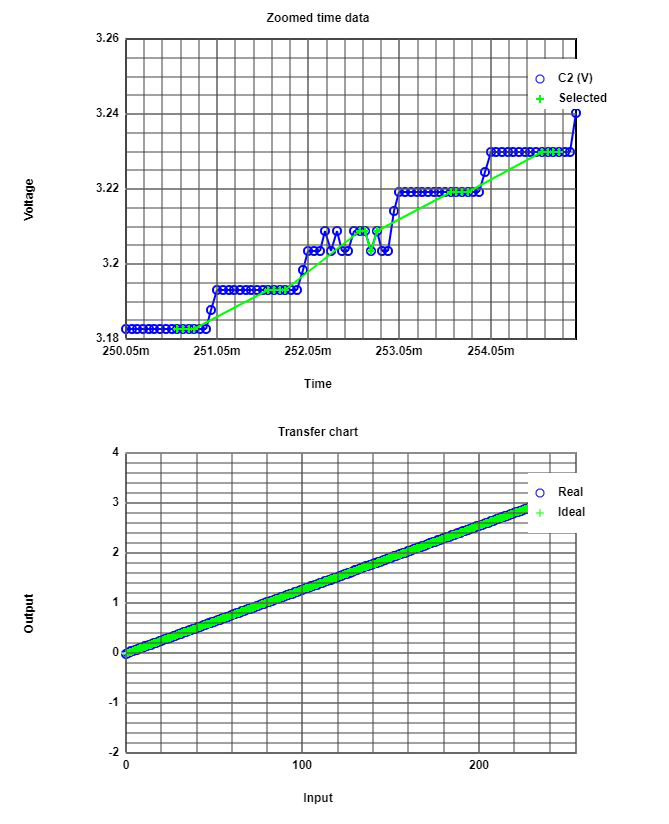
Picture 3
Ramp input
|
|
The ramp signal was generated using the "DDS" web page. Then signal was inserted to 8-bit R2R DAC circuitry inorder to analyse the INL and DNL parameters using FFT.
INL and DNL analysis (filtering of the signal)using java script tool (FFT) were performed. The INL DNL graph and values were obtained(Picture 4 and 5).
|
|
Sine measurement of R2R DAC
|
|
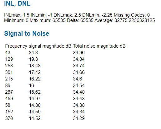
Signal was measured and SNR extracted via FFT.
From the FFT analysis, DNL max = 2.5 and DNL min = -2.25 values were observed. Therefore this is not a desirable situation and obiviously ENOB has been reduced and effectively would result a loss of some bits in output.
Picture 6
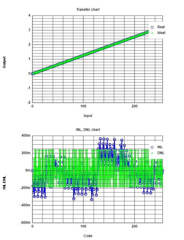
Sine measurement of digital calibrated R2R DAC
|
|
Following procedure was implimented:
Generate a calibration lookup table with ramp measurement.
Generate a new calibrated sine pattern.
Measure INL, DNL and FFT with calibrated sine pattern.
The Digital calibrated DAC gives desireble INL and DNL values (DNL in between 0.5 and -0.5) compared to the previous Sine measurements.
|
|
Conclusion
The maximum DNL value should be in between -0.5LSB and +0.5LSB for a DAC inorder to regenerate the analog signal without loosing any bits or information. The settling time should be as minimum as possible regarding to the overshoots and undershoots.
|
|
|
|
|
|
|