Hochschule Kempten      
Fakultät Elektrotechnik      
Elektronik       Fachgebiet Elektronik, Prof. Vollrath      

Data Acquisition

13.12.2022 Joerg Vollrath

+    Share page with QR-code

A high amount of high speed, high resolution data should be displayed or processed with a computer. Limits are set by the data transfer and the computing power.

BASYS 3 FPGA


The BASYS 3 FPGA board runs at 100 MHz at the 32 PMOD pins. There are serial high speed pins available, but no connector is realized supporting the speed. 100 MSps with 32 Bit per sample should be possible with his board. The XADC is only running at 1 MSps and 12 Bit.
These data can be locally processed and passed to a DAC at the 32 PMOD pins.
Data storage is present as Block RAM or external SRAM or DRAM with access times starting at 10ns. SRAM and DRAM need special memory controllers.
A serial interface over USB is provided to the PC. The VHDL code shows configuration of 230400 Baud (27 * 16 cycles), 460800 Baud (14* 16 cycles), 921600 Baud (7*16 cycles). At the moment 230400 Baud serial communication is running: 16 Bit, 5 channels, 2.9 kSps

Computer processing


A typical oscilloscope runs on a PC with a full HD resolution of 1920 x 1080 points at 25 Hz. 4 channels with at least 10 Bit vertical resolution (1024) and 48 kSps are typically be displayed. This requires a baud rate of 4 * 10 * 48 kSps = 1.8 MBaud.

Application


Serial wire and wireless comunication, video signals (30*1920*1080 pixels, 12 Bit, Full HD), audio signals (44 kHz, 24 Bit), serial interfaces (USB-C) and industrial control are typical applications.
A high number of samples is needed for video processing several video pictures requiring a large memory buffer: 10*1920*1080*12 = 248 MBit = 31 MByte.
A high number of samples is used for FFT to characterize data converters.

Acquisition strategy for this project


Figure: Transmission system

For a certain time a block of data is acquired at high speed in block memory.
Then acquisition is paused and data serially transmitted to the PC.
Then sampling is enabled again.

Realization


Block RAM is realized in the instance myBuf of module one_port_ram. Size is declared as generic.
A power of 2 size is needed to be able to easily calculate an FFT.
  generic(
    ADDR_WIDTH: integer := 16;
    DATA_WIDTH: integer:= 16
   );
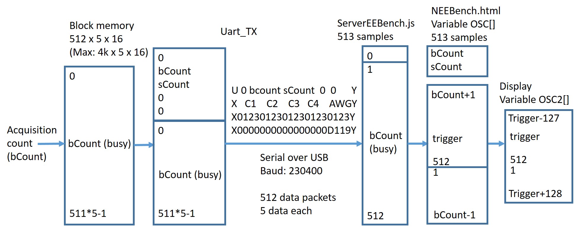
In EEBench the process storeMem controls data acquisition.
To accomodate different acquisition rates CLK, readyX (XADC conversionready) and upSample are used.
       elsif  (rising_edge(CLK) and (readyX = '1') 
                -- slow clock ??
                and (upSample = '1')
                ) then  -- continous cycling through ADC if no transmit
         if (tx_busy = '1') then  -- transfer started
            sCnt := 0;
            we <='0';
         else                    -- data sampling
          case source is
tx_busy prevents acquisition and memory write during ongoing serial transmission to the PC.
source is cycling signal generator, channel 1, 2, 3 and 4 for writing the block meory.
Current memory address (iCount), sample number (bCount) and number of sample since last transmission (sCnt) are used and bCount and sCount stored for transmission.
One sample is always invalid, since storage of individual channels can be ongoing.
Only half of the samples will be used for display.

Figure: Acquisition

uart_mem TX process is sending first information: 0, bCount, sCount,0,0.
Each packet of 5 data is surrounded by 2 characters.
The first transmission starts with U and ends wich X, all following data start with Y and end witch X.
FPGA sends 513 transmissions 5 data points 4 hex values each to the node server.
The node server (ServerEEBench.js) gathers all data and then send the data to the client web page (NEEBench.html).
At the client the data are transfered into the array OSC and then rearranged starting from bCnt+1 as 511 values.
In the valid 511 values the trigger point is searched from 511/4 until 3/4*511 and 256 values extracted and displayed. If no trigger point is found a message appears 'not triggered' and trigger point is set to 255.

Verification


  1. Simulation tb_EEBench: addrGen transition 511*5 = 2555 (x09FB) -> 5 (x0005)
  2. Simulation tb_EEBench: Transmission of 512 * 7 hexadecimal values after submission of "U"
  3. Hyperterm with Baud rate 230400 send U get 512 data hexadecimal strings
    Set block size and acquistion: O02000001
    Set sine waveform generation: S000300000F83E0F826C9B26C
    Acquire data: U
    Verification passed: 512 samples are send.
  4. ServerEEBench.js: gets 512 data pieces (cosole.log) and sends it to NEEBench.html
  5. NEEBench.html: check received data string, check bCnt, sCnt, check OSC, OSC1, OSC2
  6. Check if FFT of AWG1 at 1.40851 kHz gives SNR = - 16 * 6 dB = - 96 dB (1 V maximum input value FFFF gives 0 dB).

Variable block size


  1. Transfer block size from NEEBench to FPGA via O command:
    O<block size><sampling rate>
  2. Transfer block size from NEEBench to FPGA via O command:
    O<block size (dataMax)><time base>
    O02000004
    block size 512 (variable, signal dataMax), time base (500 us/div)
    FPGA samples with 140 cycles, 10 ns, 5 channels gives 8.32 us or fsample = 120.2 kHz
    VHDL: signal timeBase = 4 means every 4th cycle is sampled fsample = 30 kHz
  3. FPGA VHDL: if (bCnt >= 511) then .. if (bCnt >= (dataMax -1 )) then<\li>
  4. ServerEEBench: get Block size from O command, change dataMax accordingly, use dataMax for data transmission
  5. NEEBench: check that evrything is using dataMax