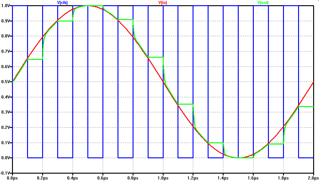
|
Vout tracks Vin for half a cycle while the switch is closed. Then the switch is opened and Vout held constant. Ideally the switch is closed for a very short time and the input voltage instantly transfered to the output. It is a RC low pass circuit.
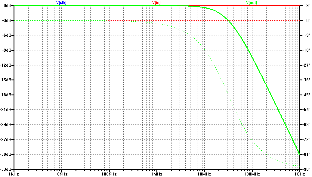
|
Nachgeladener SPICE Text Nachgeladener SPICE Text |
|
A resistor has a thermal noise density function of: \( V_{rR} \left( f \right) = \sqrt{4 \cdot k \cdot T \cdot R} \) T: absolute temperature k: Boltzman constant The rms output voltage noise can be calculated. The voltage divider gives the output voltage noise density: \( V_{out,noise} \left( f \right) = \sqrt{4 \cdot k \cdot T \cdot R} \frac{1}{1 + j \omega R C} \) The rms value can be calculated by integration over frequency as: \( V_{out,noise,rms} = \sqrt{ \int_0^{f_{3dB}\frac{\pi}{2}} V_{out,noise}^2 \left( f \right) df} \) \( V_{out,noise,rms} = \sqrt{ f_{3dB} \frac{\pi}{2} 4 k T R }\) \( V_{out,noise,rms} = \sqrt{ \frac{1}{2 \pi R C} \frac{\pi}{2} 4 k T R } = \sqrt{\frac{kT}{C}} \) Noise depends only on capacitance. For C = 1 pF and R = 10kΩ this gives 64 μV. As a rule of thumb peak to peak noise can be calculated with a factor of 6. 64 μ Vrms = 384 μ Vpp Reference: LTC signal chain seminar 2012, Noise |
RC circuit:![]() 
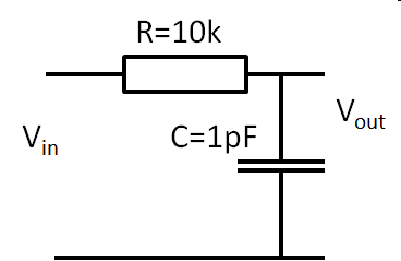
Equivalent noise circuit:
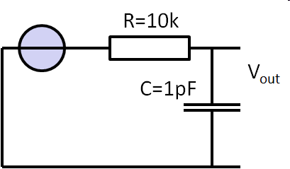
|
|
Quantization noise \( \approx \frac{LSB^2}{12} \) should be smaller than thermal noise: \( \frac{k_B \cdot T}{C} \) Giving: \( C \leq 12 \cdot k_B \cdot T \cdot LSB^2 \) \( C = 12 \cdot k_B \cdot T \cdot \frac{2^{2 \cdot N}}{V_{FS}^2} \) |
Required C as a function of data converter resolution:
|
|
\( e^{- \frac{t}{\tau}} \lt \frac{1}{2^{N}} \) \( \frac{t}{\tau} \gt ln\left(2^{N}\right) \) \( \frac{t}{R \cdot C} \gt N \cdot ln\left( 2 \right) \) The time t is limited by the sampling frequency \( f_s \). The maximum time is \( t = \frac{1}{2 \cdot f_S} \) \( R \lt \frac{1}{2 \cdot f_s \cdot C \cdot N \cdot ln\left( 2 \right)} \approx \frac{0.72}{N \cdot f_s \cdot C} \) The corner frequency of the RC circuit is: \( f_c = \frac{1}{2 \pi R \cdot C} = 0.22 \cdot N \cdot f_s \) A digital filter can correct this error. |
Required R with VFS = 1 V as a function of data converter frequency:
|
|
Pass gate: NMOSFET VDD - Vth >> V otherwise Ron depends on Vin Transfer gate: NMOSFET parallel to PMOSFET Need CLK and /CLK with timing matching |
|
Effect of clock jitter on sampling of a sine signal: V(t) = A sin(ω t ) = A sin( 2 π fsig t ) A: Amplitude fsig: sine signal frequency Calculate the maximum difference of the voltage level with a jitter dt. The maximum slope of the signal is: V'(t) = A 2 π fsig sin( 2 π fsig t ) V'(t) = A 2 π fsig The voltage difference &Delta V = A 2 π fsig dt should be smaller than 0.5 LSB A 2 π fsig dt < 0.5 LSB The amplitude is: A = 2N - 1 LSB The maximum signal frequency is: \( f_{sig,max} = \frac{f_{sample}}{2} \) This gives for dt: \( dt < \frac{LSB}{2 \cdot A \cdot 2 \pi \cdot f_{sig,max}} \) \( dt < \frac{LSB}{2 \cdot 2^{N-1} LSB \cdot 2 \cdot \pi \cdot \frac{f_{sample}}{2}} \) \( dt < \frac{1}{ 2^{N} \cdot \pi \cdot f_{sample}} \) |
|
| If the clock jitter is uncorrelated to the input signal it gives white noise. |
|
MOSFET switch:
|