Interface ElectronicsInterface electronics deals with data converters. Data converters are very interesting electronic systems combining digital, analog electronics and signal processing. |
|

6.10.2025
📹 Video Introduction 7.10.2020
1. Introduction
- Analog versus digital, data converter systems
- Data converter metrics:
- N, Vref, Vfs, Vmax, LSB
📹 Video Introduction 7.10.2020
8.10.2025
📹 Video LTSPICE 12.10.2020
2. LTSPICE
- Installation and Operation
- Behavioral models of AD converters and DA converters
📹 Video LTSPICE 12.10.2020
13.10.2025
📹 Video INL and DNL 14.10.2020
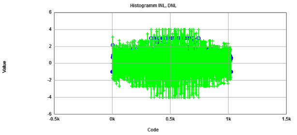
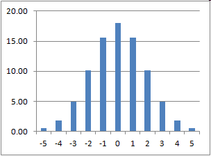
3. Static errors and measurement
- INL, DNL, offset, gain error
- INL, DNL example
- INL, DNL histogram testing
📹 Video INL and DNL 14.10.2020
20.10.2025, 27.10.2025
Reading: CMOS: Circuit Design, Layout and Simulation, Baker, Chap.28, p.953-957
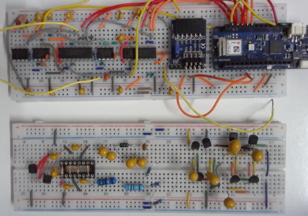
📹 Laboratory 21.10.2020 Web report and ADC DAC simulation
📹 Lecture 23.10.2020 Spectral test
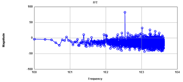
4. Spectral Test
- Quantization Error
- Dynamic characteristic: spectrum analysis
- Sampling
- Aliasing
- FFT, SNDR
Reading: CMOS: Circuit Design, Layout and Simulation, Baker, Chap.28, p.953-957
📹 Laboratory 21.10.2020 Web report and ADC DAC simulation
📹 Lecture 23.10.2020 Spectral test
3.11.2025
Reading: CMOS: Circuit Design, Layout and Simulation, Baker, Chap.29, p.965-984
📹 Lecture 26.10.2020 DAC architectures
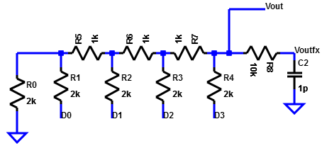
5. DAC architecture
- R string
- Charge Scaling
- Interpolating, segmented and split array architectures.
- R2R and C2C architectures
Reading: CMOS: Circuit Design, Layout and Simulation, Baker, Chap.29, p.965-984
📹 Lecture 26.10.2020 DAC architectures
10.11.2025
Reading:
Link:
📹 Lecture 28.10.2020 DAC errors
6. Errors in Practical Realization
- Systematic Errors
- Statistical Errors and Mismatch
- Impact on INL and DNL
- DAC Calibration
Reading:
Link:
📹 Lecture 28.10.2020 DAC errors
17.11.2025
Link:
📹 Lecture 2.11.2020 DAC practical considerations
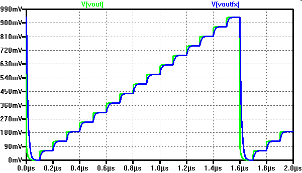
7. DAC practical considerations
- Settling time
- Spurios signal coupling
- Timing error
- Reconstruction filter
- Implementation Examples
Link:
📹 Lecture 2.11.2020 DAC practical considerations
24.11.2025
Sampling and Jitter
Reading:
📹 Lecture 4.11.2020 ADC Architectures, sampling, jitter
8. Analog to digital converters (ADC)
Sampling and Jitter
- Sampling: Resistance, capacitance, jitter
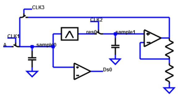
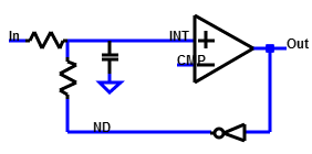
- Single slope and dual slope ADC
Reading:
📹 Lecture 4.11.2020 ADC Architectures, sampling, jitter
1.12.2025
Reading: CMOS: Circuit Design, Layout and Simulation, Baker, Chap 29, p.985-1007
📹 Lecture 25.11.2020 Flash and SAR ADC
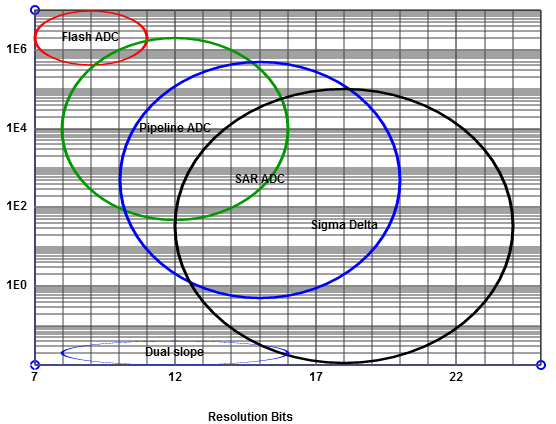
9. Basic ADC Architectures
- Flash ADC
- Folding flash ADC
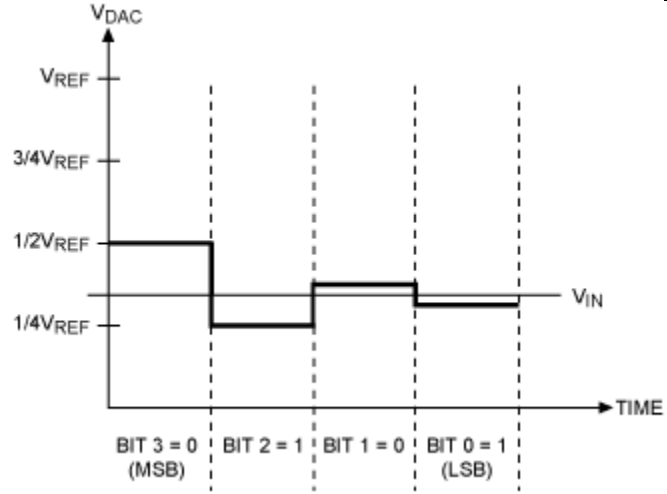
- Successive approximation (SAR) ADC
- Building a successive approximation (SAR) ADC
Reading: CMOS: Circuit Design, Layout and Simulation, Baker, Chap 29, p.985-1007
📹 Lecture 25.11.2020 Flash and SAR ADC
8.12.2025
Reading:
CMOS: Circuit Design, Layout and Simulation, Baker, Chap 29, p.994-998
CMOS Analog Circuit Design, Allen, Holberg, Chap 10, p.612-729
📹 Video Pipeline ADC 16.12.2020
10. Pipeline ADC start
- Building blocks and simulation of a pipeline AD converter.
Reading:
CMOS: Circuit Design, Layout and Simulation, Baker, Chap 29, p.994-998
CMOS Analog Circuit Design, Allen, Holberg, Chap 10, p.612-729
📹 Video Pipeline ADC 16.12.2020
15.12.2025
Reading:
11. Pipeline ADC details
- Building a pipeline AD converter for a laboratory
- Offset, gain and random errors of a pipeline AD converter.
- 1.5 Bits per stage pipeline ADC
- Calibration
Reading:
21.12.2025
Reading:
📹 Lecture 1.12.2020 Sigma Delta ADC
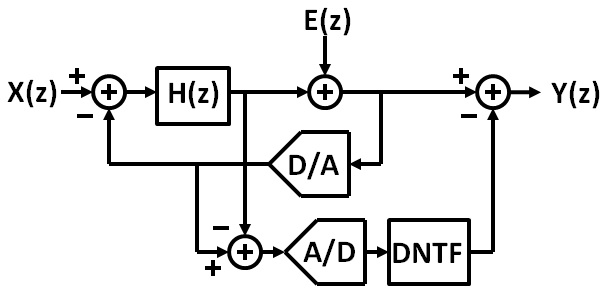
12. Oversampling ADC
Sigma delta ADC, PWM- Passive 1st order sigma delta ADC
Simulation example - Active first order sigma delta ADC with decimation filter
- Active second order sigma delta ADC with decimation filter
Reading:
📹 Lecture 1.12.2020 Sigma Delta ADC
12.1.2026
Sigma delta ADC, PWM
Reading:
📹 Lecture 9.12.2020 Advanced Sigma Delta ADC
13. Advanced sigma delta ADC
Sigma delta ADC, PWM
- MASH 2-1 sigma delta ADC with Decimation filter
Reading:
📹 Lecture 9.12.2020 Advanced Sigma Delta ADC
\( FOM = \frac {Power}{f_{sample} \cdot 2^{NBit}} \)
19.01.2026
Laboratory 12 and Summary
Reading:
14. Summary and Outlook
- Figure of Merit for ADCs
- Noise in data converters
- Interfaces
Laboratory 12 and Summary
Reading:
Excercise:
Interface Electronics Problems