Pipeline ADC circuit: Overview
This simulation contains static CLK for simulating transfer characteristic.
Dynamic CLK statements are used for normal operation generating serially 8 bit at Dout.
Generating a positiv digital signal from 0V to 3V req8bit_Pipeline_Sim_Transferuires R3 and R4 connected to VDDp.
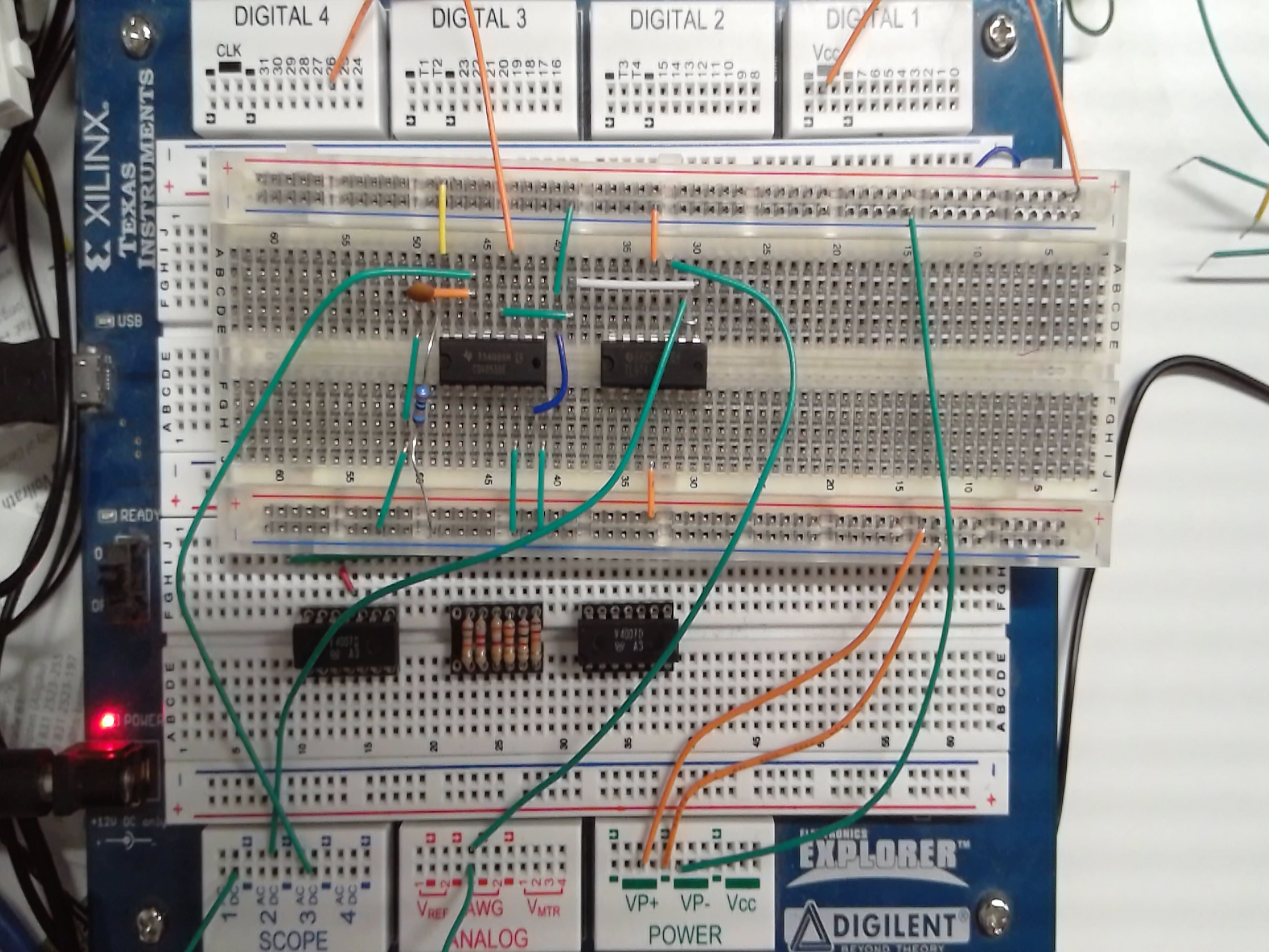
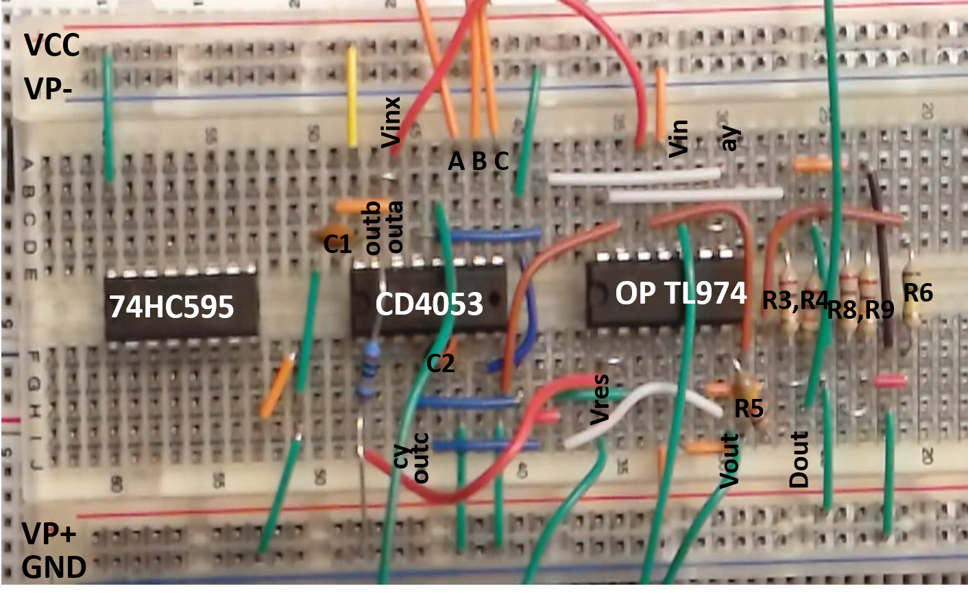
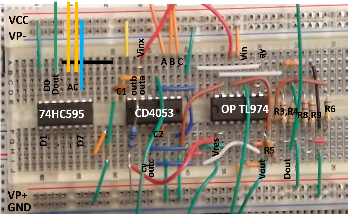
On the left are the 2 switches selecting input voltage V(in) or V(res) from a pipeline stage operation.
The voltage Vin is saved as Vinx on sample and hold capacitor C1.
The comparator X3 generates data output Dout.
Vout = 2 * Vinx - Dout is generated by X1 and saved via a switch on C2 as Voutx. Buffer X6 feeds VoutX as residue Vres back to the input for the next cycle.
CLK 1 is shortly activated to sample V(in) and generate the first Dout. For the number of required bits CLK2 and then CLK 3 is activated generating the remaining bits.
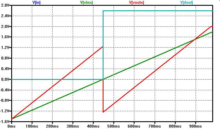
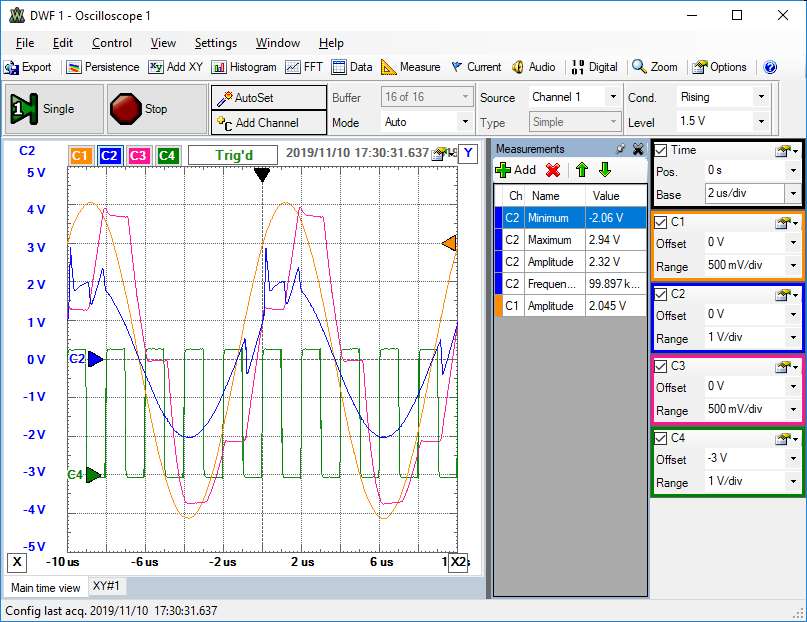
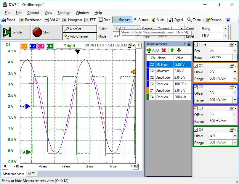
A dout signal 0V..2.6V is generated.
Input range is from -1.44V up to 1.44v.
There will be missing codes due to output voltages at the switching point of:
1.128V..-1.128 V.
The rounded shape of dout caused by the diodes in the opamp model will give wrong codes at the transition.
A real opamp can avoid this, but can introduce a feedback loop to Vintx via opamp X1.
The comparator opamp model has to include an inverter output stage and a separate sample and hold for Vinx for gain is needed to prevent feedback oscillation.
Dynamic CLK statements are used for normal operation generating serially 8 bit at Dout.
Generating a positiv digital signal from 0V to 3V req8bit_Pipeline_Sim_Transferuires R3 and R4 connected to VDDp.
On the left are the 2 switches selecting input voltage V(in) or V(res) from a pipeline stage operation.
The voltage Vin is saved as Vinx on sample and hold capacitor C1.
The comparator X3 generates data output Dout.
Vout = 2 * Vinx - Dout is generated by X1 and saved via a switch on C2 as Voutx. Buffer X6 feeds VoutX as residue Vres back to the input for the next cycle.
CLK 1 is shortly activated to sample V(in) and generate the first Dout. For the number of required bits CLK2 and then CLK 3 is activated generating the remaining bits.
- Simulate a ramp signal with static CLKs and discuss the transfer characteristic.
Comment out the .save command to see all signals.
Activate the CLK PULSE statements and deactivate th static CLK DC statements. - Use the ramp signal for calibration
- Simulate a sine signal and calculate SNR, ENOB
- Simulate a sine signal and calculate SNR, ENOB with calibration
A dout signal 0V..2.6V is generated.
Input range is from -1.44V up to 1.44v.
There will be missing codes due to output voltages at the switching point of:
1.128V..-1.128 V.
The rounded shape of dout caused by the diodes in the opamp model will give wrong codes at the transition.
A real opamp can avoid this, but can introduce a feedback loop to Vintx via opamp X1.
The comparator opamp model has to include an inverter output stage and a separate sample and hold for Vinx for gain is needed to prevent feedback oscillation.
- How do CLK1, CLK2 and CLK3 control operation?
How many bits are generated? - How many samples are simulated?
- What is the resolution of INL, DNL calculation with this number of samples?
- Optimize the simulation and extract INL and DNL
CLK1 controls the sampling every 480µs.
CLK2 and CLK have a cycle of 60µs.
480/60 = 8 bits.
This is a 8-bit pipeline ADC.
The transient simulation is done for 983.4ms.
983.4ms/480µs = 2048
2048 samples are generated.
Read raw file should have a step size of 480µs.
The DAC has a Vref of VDDp = 3 V and a resolution of 8-bit.
LSB = 3/256 V = 0.01171875 V.
VDD = 2V
LSB = 2/256 V = 0.0 V.
Simulation gives 7mV step size due to RC limits?.