Platform Hardware
|
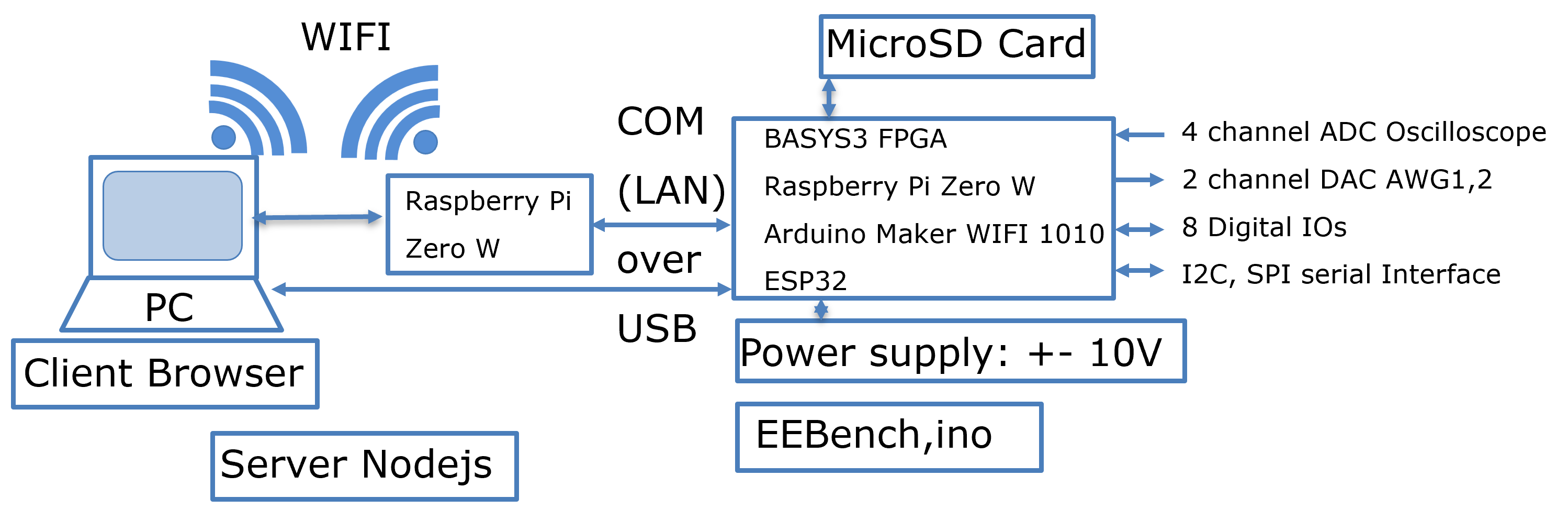
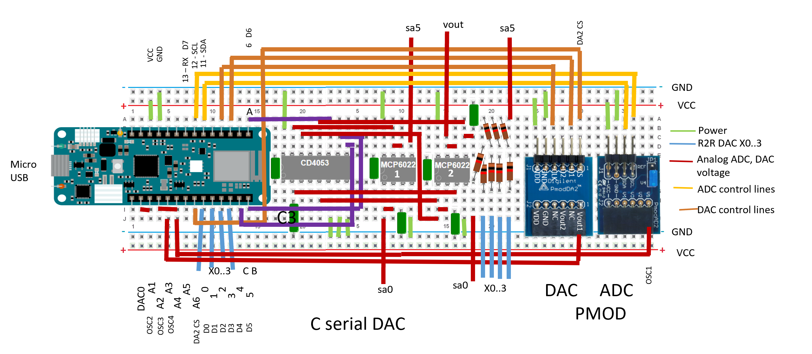
Arduino (BASYS3, Rpi) Breadboard, PMOD DA2, AD2 Scalable R2R DAC, (8-Bit R2R DAC, C serial DAC, Rstring, Interpolating DAC) (SAR ADC, pipeline ADC) |
  |
Platform Software PC
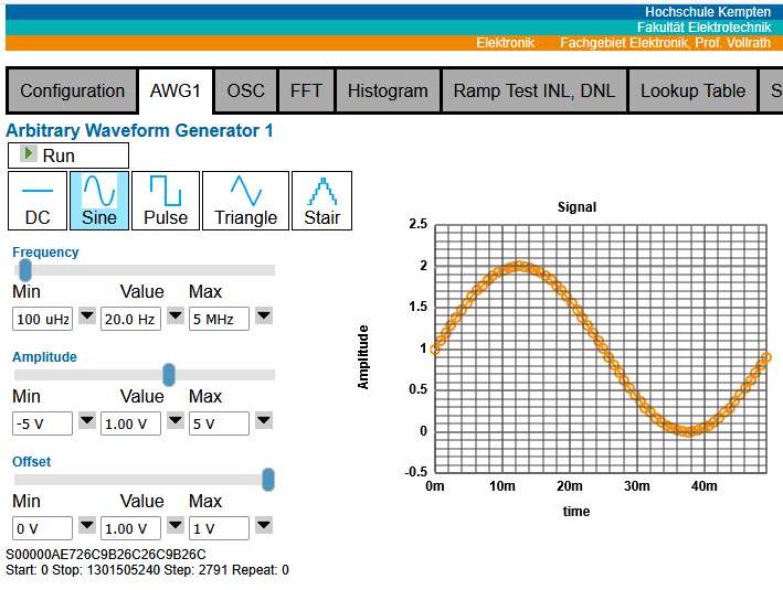
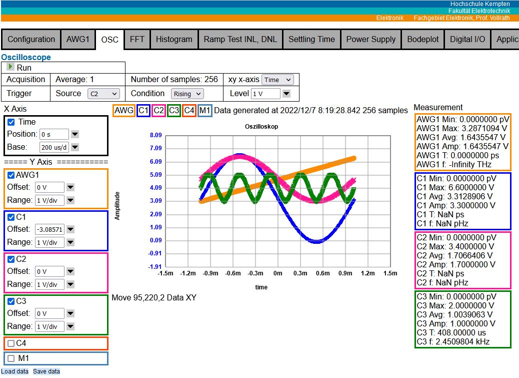
Software PC (Rpi)User Interface: Browser: Projekte/NEEBench.html Server NodeJS: NodeEEBench.bat ServerEEBench.js User Interface: Browser: Projekte/SerialA.html Server NodeJS: StartServerAx.bat ServerAx.js |
|
Synchronized with Arduino Software
Software Arduino
C serial DAC
Arduino/DataConverterCharV5/DataConverterCharV5.ino
R2R DAC
Arduino/DataConverterChar
Cyclic R2R DAC Schematic
|
The schematic shows a cyclic R2R DAC. A SH at the left side for the starting voltage added to a 4 bit R2R DAC. The output goes to buffer amplifier and SH to generate sa0. This level can be fed back to the left input SH. The final value is sampled on the right and gives Vout. |
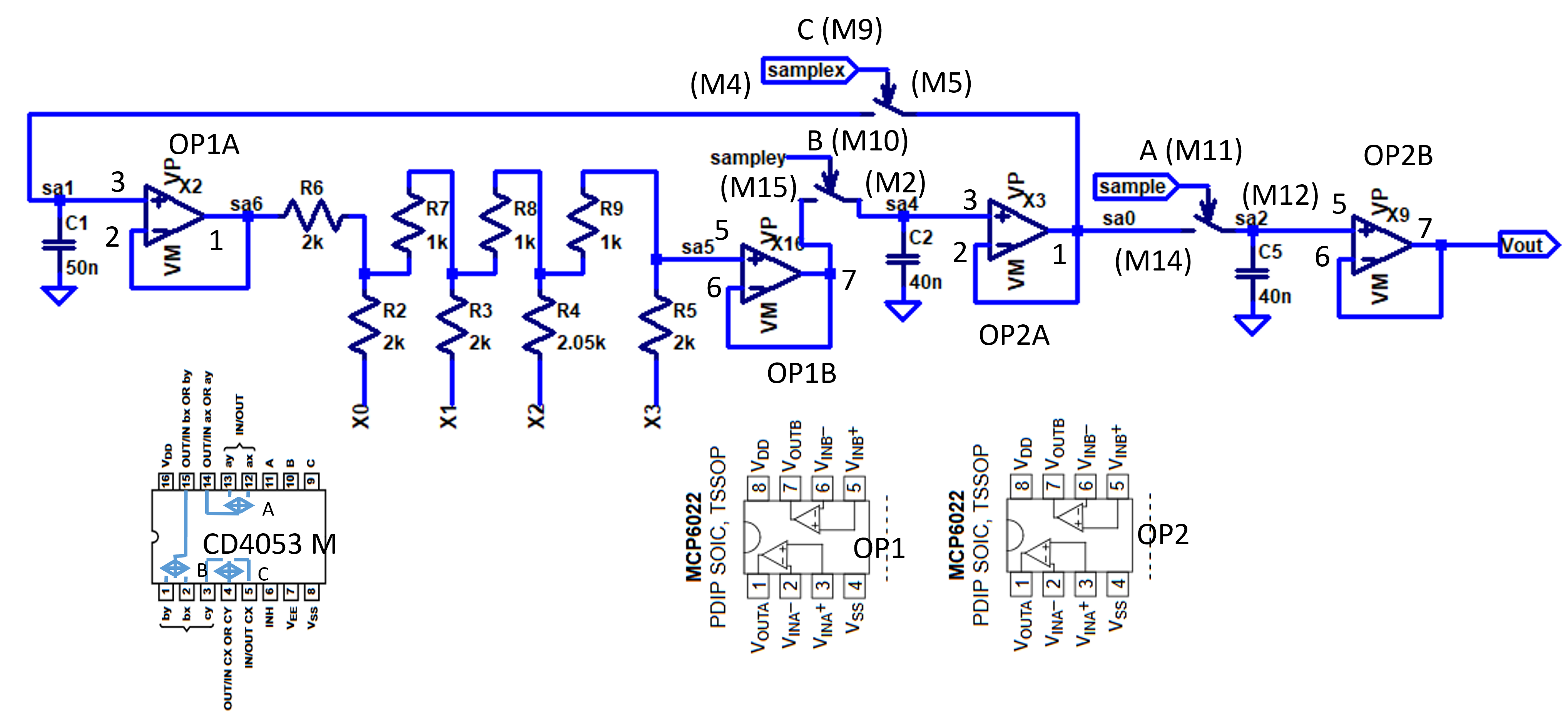 The resolution NBit can be controlled via software. |
It is easy to scale this architecture via software.
Tradeoff between timing and resolution.
Arduino Schematic component
0 D0, X0
1 D1, X1
2 D2, X2
3 D3, X3
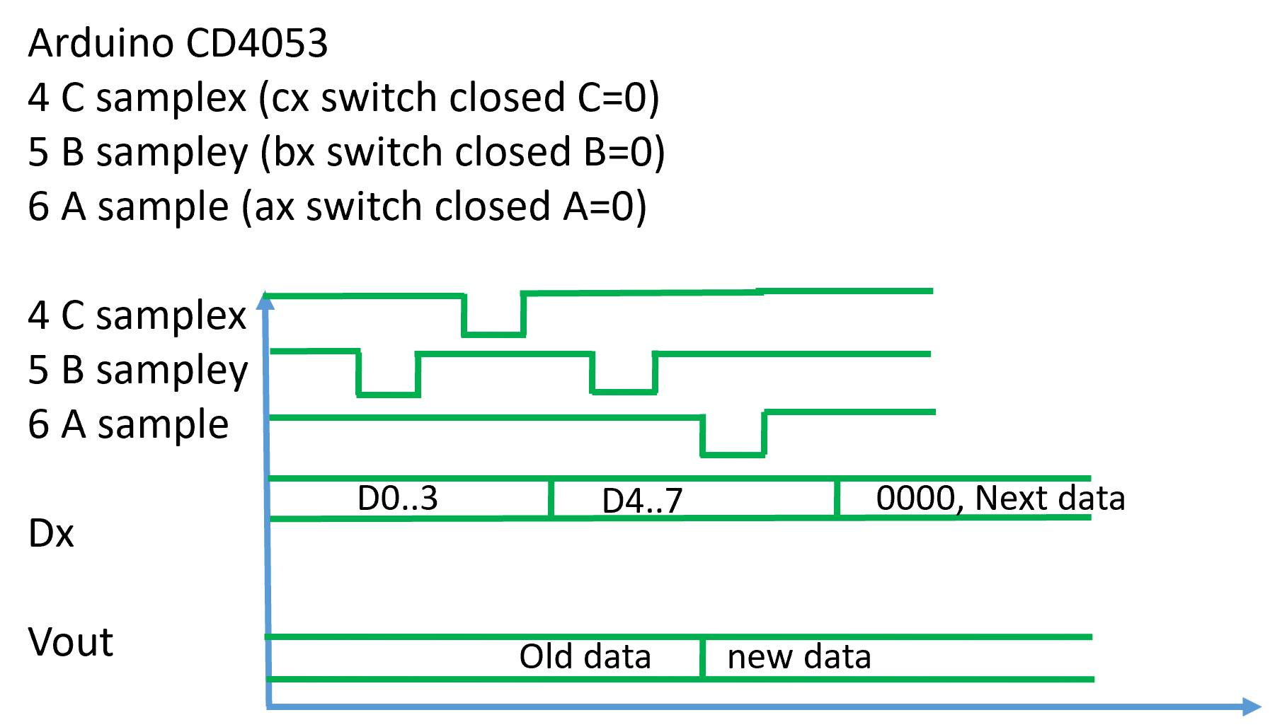
4 C samplex (cx switch closed C=0) Pin 9 CD4053
5 B sampley (bx switch closed B=0) Pin 10 CD4053
6 A sample (ax switch closed A=0) Pin 11 CD4053
Pin 6 CD4053 Inhibit 0 V
Pin 7 CD4053 VEE 0 V
Pin 8 CD4053 VSS 0 V
Pin 16 CD4053 VDD 5 V
Pin 4 MCP6022 GND 0 V
Pin 7 MCP6022 VDD 5 V
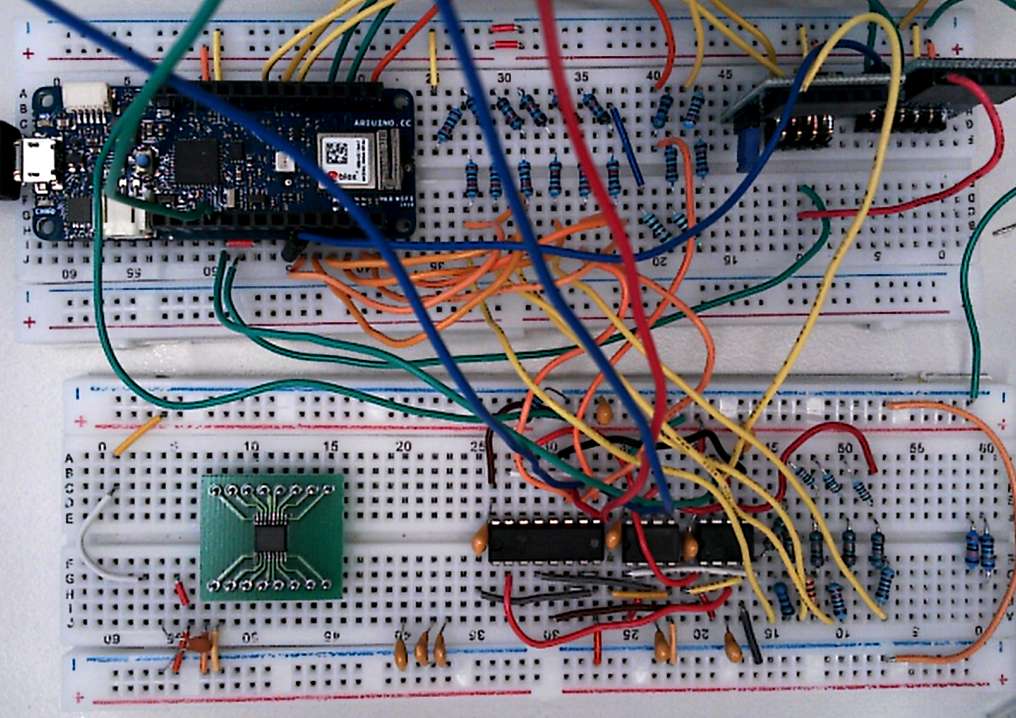
90 min from schematic to Breadboard.
At the start once a D = 0000 can be set for intialization.
This is not mandatory.
In the LTSPICE schematic a samplez signal connects the input to gnd.
An Arduino pin could be used for initialization having tri state as input and 0V, gnd as output.
Capacitance: start 40nF, 2nd try 1nF, check CD4053, MCP6022 60 pF
Thermal Noise minimum capactitance:
NBit = 16, VFS = 3.3 V, Cmin = 20 pF, per zusätzlichen Bit Faktor 4 in C
NBit = 20, VFS = 3.3 V, Cmin = 5.3 nF
Bypass, decoupling capacitance: 1 uF, 0.1 uF = 100nF, 10 nF
New sketch: C:\temp\NodeEEBench\DACCharCyclic\DACCharCyclic.ino
12 bit R2R DAC
Tradeoff between timing and resolution.
Arduino Schematic component
0 D0, X0
1 D1, X1
2 D2, X2
3 D3, X3
4 C samplex (cx switch closed C=0) Pin 9 CD4053
5 B sampley (bx switch closed B=0) Pin 10 CD4053
6 A sample (ax switch closed A=0) Pin 11 CD4053
Pin 6 CD4053 Inhibit 0 V
Pin 7 CD4053 VEE 0 V
Pin 8 CD4053 VSS 0 V
Pin 16 CD4053 VDD 5 V
Pin 4 MCP6022 GND 0 V
Pin 7 MCP6022 VDD 5 V
90 min from schematic to Breadboard.
At the start once a D = 0000 can be set for intialization.
This is not mandatory.
In the LTSPICE schematic a samplez signal connects the input to gnd.
An Arduino pin could be used for initialization having tri state as input and 0V, gnd as output.
Capacitance: start 40nF, 2nd try 1nF, check CD4053, MCP6022 60 pF
Thermal Noise minimum capactitance:
NBit = 16, VFS = 3.3 V, Cmin = 20 pF, per zusätzlichen Bit Faktor 4 in C
NBit = 20, VFS = 3.3 V, Cmin = 5.3 nF
Bypass, decoupling capacitance: 1 uF, 0.1 uF = 100nF, 10 nF
New sketch: C:\temp\NodeEEBench\DACCharCyclic\DACCharCyclic.ino
12 bit R2R DAC
| Rx | Cx | activeS | offS | INL, DNL max 255 | INL, DNL max 1024 |
| Rx | Cx | activeS | offS | INL, DNL max 255 | INL, DNL max 1024 |
| Rx | Cx | activeS | offS | INL, DNL max 255 | INL, DNL max 1024 |
CTRL Signal Timing at Breadboard
 |
 |
Sampling capacitances: C1, C2, C5 = 50 pF
Decoupling, bypass capacitances: CdecouplingIC = 70nF, Cdecouplingpower = 400 nF
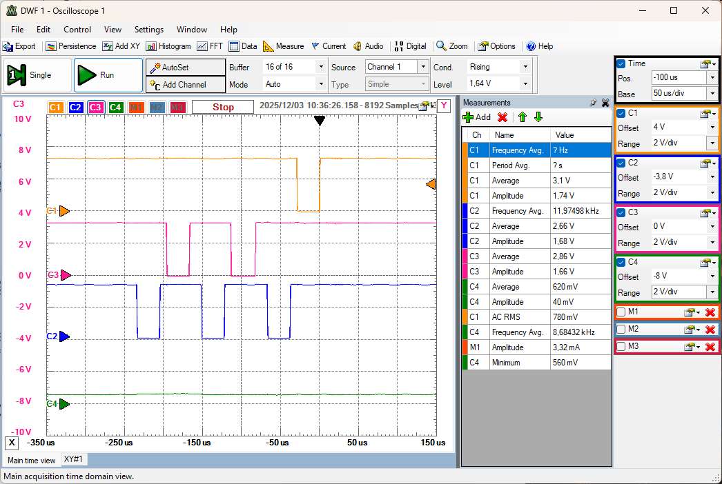
Control signals for a 12-Bit cyclic R2R DAC
C1 orange sampling, C2 blue sampley, C3 red samplex
A new sample is acquired with: tcycle = 4.6 ms, fcycle = 200 Hz
For acquisition each cycle has the switch on 20 us and 5 us pause between switch activations.
12 Bit acquisition takes 3 cycles with 2 switch operations giving a total of 6*25us = 150 us
More Data Converter Circuits
|
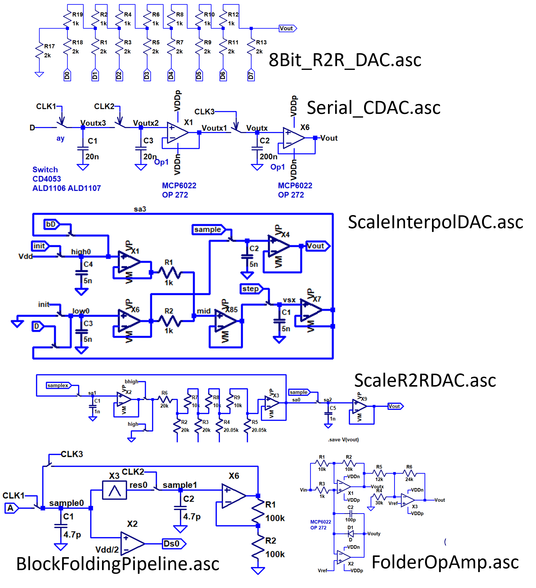 |
- 8-Bit R2R DAC: 8Bit_R2R_DAC.asc
- Scalable C serial DAC: Serial_CDAC.asc
- Scalable R2R DAC: ScaleR2RDAC.asc
- Scalable interpolating DAC: ScaleInterpolDAC.asc
- Scalable interpolating DAC SAR ADC: BlockCserialSARADC_01.asc
- Scalable folding pipeline ADC:
BlockFoldingPipeline.asc,
FolderOpAmp.asc
- 8 Bit mixed DAC: 8Bit_RLR2RMix_DAC2.asc
- Sigma Delta ADC (FPGA)