Design of an integrated pipeline ADC
Figure 1: LTSPICE BlockFoldingPipeline.asc
Overview
Layout starting library for Electric VLSI system:
Pipeline.jelib
Basic layout library for synthesis:
sclib.jelib
LTSPICE models:
cmosedu_models.txt
- Transistor performance limits
- Static IDS(UDS,UGS) with typical W, fixed minimum L of PFET and NFET gives IDSmax, Vth, λ
- Inverter chain with some Ws, and fixed minimum L and optimum operation point simulate
transient. Find the DC bias for input where the output voltage is equal to input voltage.
Calculate resistance Ronp, Ronn for sample and hold circuit.
With this DC value and AC voltage do AC Analysis to find transit frequency ft
and maximum gain Aol.
Calculate input capacitance Cin.
- Ring oscillator (3 inverter stages) to measure fRing.
- Amplifier architectures
- Single ended: Common Source amplifier with biased active load
- Single ended: Common Source amplifier with biased load
- Single ended: Common Source amplifier with MOSFET diode load
- Single ended: Inverter amplifier
- Single ended: Inverter with transfer gates resistors as feedback
- Differential: external biased
- Differential: internal biased
- Differential: MOSFET diode load
- Lowpoer and high speed
- Sample and hold
- Dimension of C
- Gate current leakage compensation necessary?
- Gate current leakage measurement?
- Coupling of clock to output.
- Clock generation with ring oscillator.
- Signal analysis improvement with low pass or ideal sample and hold
to suppress spikes from switching.
- Comparator
- Folder
- C2C/R2R DAC for biasing
- Shift register for output data
- Assemble Circuit
- Calibrate comparator and residue
- Simulate ramp
- Sampling at maximum speed and average speed (100MHz)
- Output codes 10 times 2B number of bits to get DNL, INL accuracy of 0.1.
- Generate error correction lookup table.
- Measure power consumption
- Simulate sine signal
- Integer prime number (13,101) of periods of full input range
- Output codes bigger than 10(?) times 2B number of bits
- Sampling at maximum speed and average speed (100MHz)
- Measure power consumption
- Process data with error correction
- Since there will be missing codes and non linearities error
correction can be done based on the ramp simulation
Duration
Specification
Target technology: 50nm
(1) Power supply: 1V
This gives minimum power consumption and can be integrated in 50nm technology.
(2) Sampling speed: ft/2, fringosci.
(3) Resolution: 16 bit (20 bit)
(4) Low power
Since the design should be as fast as possible a ringoscillator is used as starting point for clock generation.
A clock divider using always on sample and hold circuits can be incorporated to lower clock frequency.
Description
Starting point is the circuit below which was realized during a practical laboratory.
LTSPICE schematics: (Vorlesung/Einzelvorträge/20xx_PipelineADC/BlockFoldingPipeline.asc using SampleHold.asc, Folder.asc, Comparator.asc
PipeReal.asc
Figure 2: Circuit diagram (Click on picture to see LTSPICE drawing code)
The left shows the sample and hold switches selecting the external signal or the internal residue for
seriell conversion.
The top shows the signal path with the second sample and hold after the folder and
before the second amplifier.
The signal path is buffered with 0.5pF.
The power supply is buffered with 474nF.
The bottom path shows the digital path to compare the input signal.
Modifications:
- 50nm transistor models
- 50nm unit transistors are used scaled with integer number N in parallel
- Resistors will be replaced with transfer gates
- Reference for comparator will be DAC output for calibration
- Gain will be controlled with DAC output for transfer gates of feedback circuits
- Sample and hold with clock coupling compensation transistors
- Differential folding circuit and comparator (Dummy circuit)
State of the art
Review of 10 recent pipeline ADC publication from IEEE solid state circuits into References section.
Discuss performance data of these architectures (technology, area, power, speed, resolution).
Discuss basic circuits: Opamp, comparator and sample and hold.
Transistor performance limits
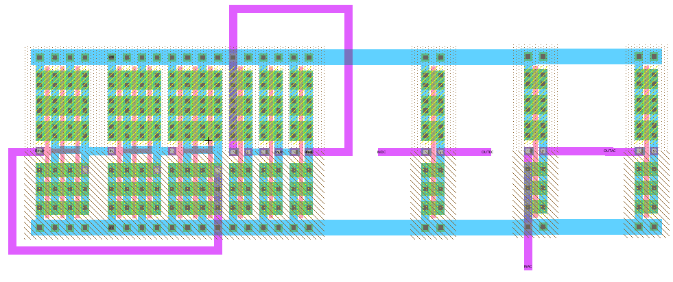
Figure 3: Layout in Electric of 2 3 stage ring oscillators, an inverter for IV curves and an inverter with load for AC analysis
Static IV curves for PFET and NFET
The structure Xinv_3x1@3 has 3 PFETS in parallel L=50nm W=250nm and 3 NFETs in parallel with L =50nm and W=25 nm.
Input is pin INDC and output OUTDC.
Measureing a transfer characteristic IDS(VGS) gives Vth, RDSon and IDSmax.
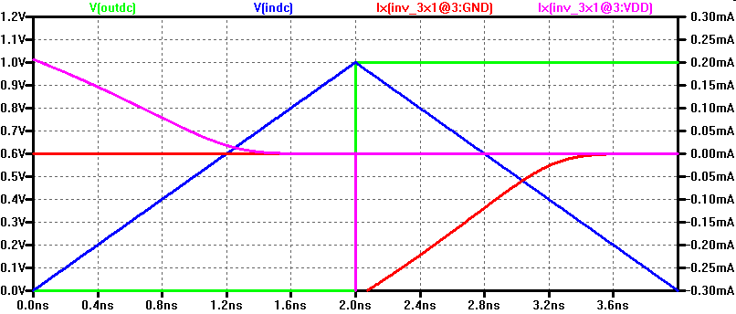
When OUTDC=0V and INDC goes from 0 to 1V the PFET is turned of and Ix(inv_3x1@3:VDD) gives the PFET source drain current.
IDSPmax = -206 uA, Vthp = -300mV, IDSNmax = 316uA, Vthn = 300mV.
RDSPon = U/I = 1V/206uA = 5 kΩ RDSNOn = 1V/316uA = 3.16 kΩ
AC analysis for inverter chain
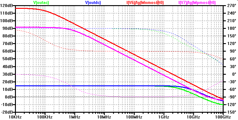
OUTAC shows a 3dB corner frequency of 3 GHz with a gain of s0 log(5.3) = 14.6 dB.
Ring oscillator performance: frequency and power consumption
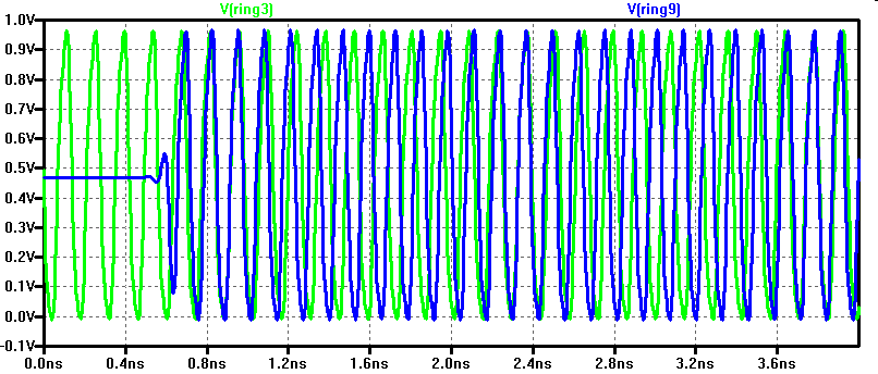
It shows 7 GHz oscillation frequency. With 149uA (Ring3) and 447uA (Ring9) power consumption.
The ring oscillator will be used to generate a clock for sampling.
Sampling Network thermal noise
\( C \gt 12 \cdot k_B \cdot T \frac{2^{2 B}}{V_{FS}^{2}} \)
kB: Boltzmann constant
T: absolute temperature in Kelvin
B: number of Bits
VFS: Full scale voltage
| B | Cmin(VFS=3.3V) |
Cmin(VFS=1V) |
| 8 | 0.3 fF | 0.003 pF |
| 12 | 80 fF | 0.8 pF |
| 16 | 20.6 pF | 206 pF |
| 20 | 5.28 nF | 52.8 nF |
| 24 | 1.32 uF | 13.2 uF |
Table: Required C as function of ADC resolution and full scale voltage
Adding 4 bits required an increase in capacitance by a factor of 256.
Decreasing the voltage by a factor of 3.3 increases the capacitance with a factor of 10.
16 bit requires 206 pF at 1V full scale.
To make sure the error of the RC network at 7 Ghz is less than 1/2LSB:
\( R \lt \frac{0.72}{B \cdot f_s \cdot C} \)
fs: Sampling frequency (half period active and switch closed)
B : number of bits
C: sampling capacitance
R (7 GHz, 16 Bit)= 0.031 Ω
| B, C | fS = 10MHz |
fS = 100MHz |
fS = 1GHz |
| 8, 3 fF | 3MΩ | 300 kΩ | 30 kΩ |
| 12, 0.8 pF | 7.5kΩ | 750 Ω | 75 Ω |
| 16, 206 pF | 21.8 Ω | 2.18 Ω | 0.22 Ω |
| 20, 52.8 nF | 70 mΩ | 70 mΩ | |
| 24, 13.2 uF | 2.3 mΩ | 230 μΩ | |
Table: Required R as function of ADC resolution and speed for VFS=1V
Since these values are very low and can not be realized,
higher values are used and a digital filter or error correction is required to adjust
the frequency response.
This process with the measured RDSon in the range of kΩ can easily achieve:
1GHz, 10 Bit;
100 MHz, 12 Bit;
10 MHz, 14 Bit;
References
[1] Murmann, EE315B - Analog Digital Conversion Circuits, https://web.stanford.edu/group/murmann_group/cgi-bin/mediawiki/index.php/Boris_Murmann
[2] Haideh Khorramabadi , EE247 Analog-Digital Interface Integrated Circuits, http://inst.eecs.berkeley.edu/~ee247/fa09/index.html
[3] Baker, ECE 615 CMOS Mixed-Signal IC Design, Spring 2009, http://www.cmosedu.com/jbaker/courses/ece615/s09/lec615.htm
[4] P. E. Allen, D.R. Holberg, CMOS Analog IC Design, http://www.aicdesign.org/scnotes10.html
[1] Yong L.; Michael P. F., "A 1 mW 71.5 dB SNDR 50 MS/s 13 bit Fully Differential Ring Amplifier Based SAR-Assisted Pipeline ADC" Solid-State Circuits,
IEEE Journal of, vol.50, no.12, pp. 2901,2911, December 2015
[2] Chen-K.H.; T.C. Lee; "A Single-Channel 10-b 400-MS/s 8.7-mW Pipeline ADC in a 90-nm Technology" Solid-State Circuits, IEEE Asian Conference of,
INSPEC Accession Number: 15728345, pp. 1,4, November 2015
[3] Yong L.; Michael P. F., "A 100 MS/s, 10.5 Bit, 2.46 mW Comparator-Less Pipeline ADC Using Self-Biased Ring Amplifiers" Solid-State Circuits, IEEE
Journal of, vol.50, no.10, pp. 2331,2341, October 2015
[4] Rohan S.; Frank v. d. G.; K. Bult; "A 12 b 53 mW 195 MS/s Pipeline ADC with 82 dB SFDR Using Split-ADC Calibration" Solid-State Circuits, IEEE
Journal of, vol.50, no.7, pp. 1592,1603, July 2015
[5] James L.; Daehwa P.; S. Lee; Masaya M.; Akira M.; "An Ultra-Low-Voltage 160 MS/s 7 Bit Interpolated Pipeline ADC Using Dynamic Amplifiers" Solid-
State Circuits, IEEE Journal of, vol.50, no.6, pp. 1399,1411, June 2015
[6] Yanwei W.; X. Peng; Yang D.; M. Liu; "Analysis and design of double nesting gain boosted amplifier in 14 bits 50MS/S pipeline ADC" Solid-State and
Integrated Circuit Technology, IEEE International Conference of, INSPEC Accession Number: 14870694, pp. 1,3, October 2014
[7] Manar E. C.; X. Li; S. Kimura; K. Maclean; J. Hu; Mark W.; Matthew G.; Scott K.; Robert P.; Charles K. S.; William B.; "A 12 Bit 1.6 GS/s BiCMOS 2×2
Hierarchical Time-Interleaved Pipeline ADC" Solid-State Circuits, IEEE Journal of, vol.49, no.9, pp. 1876,1885, September 2014
[8] D. Y. Chang; Carlos M.; Denis D.; S. K. Shin; Kevin G.;Thomas T.; H. S. Lee; Kush G.; Matthew S.; "A 21mW 15b 48MS/s Zero-Crossing Pipeline ADC in
0.13µm CMOS with 74dB SNDR" Solid-State Circuits, IEEE International Conference of, INSPEC Accession Number: 14147497, pp. 204,205, February 2014
[9] Jiangfeng W.; C. Y. Chen; T. Li; Lin H.; W. Liu; W. T. Shih; Shauhyuarn S. T.; B. Chen; Chun S. H.; Bryan J. J. H.; Hing T. H.; Steven J.; Loke K. T.; Hung
V.; "A 240-mW 2.1-GS/s 52-dB SNDR Pipeline ADC Using MDAC Equalization" Solid-State Circuits, IEEE Journal of, vol.48, no.8, pp. 1818,1828, August
2013