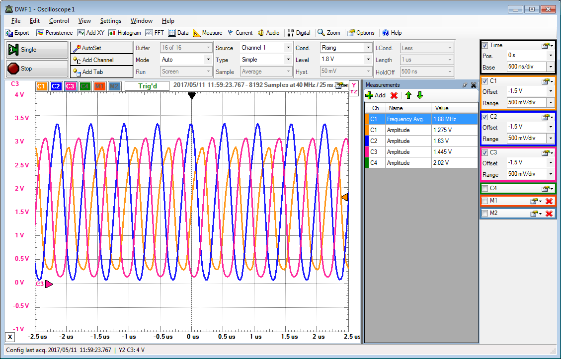
A 5..8 Bit 500Hz embodiement of a Pipeline ADC

List of parts


Electronic Explorer Board ($ 330 / $660)
Nexys 3 Board ($ 190 / $270)
3 ALD1106 4 NFETs (Digikey)
3 ALD1107 4 PFETS (Digikey)
4 Potentiometers 150k
10 Capacitors (Signal)
10 Capacitors (Power)
Breadboard PCB like Electronic Explorer (EBay)

VHDL Files for Nexys 3 Board for Spartan 6, XC6SLX45, Package CSG324
VHDL Files for Nexys 3 Board for Spartan 6, XC6SLX45, XC6SLX16, Package CSG324 with buffer and test

Duration


2 days

Description


A pipeline ADC circuit is built on a PCB board and tested with the Electronic Explorer as a signal generator and a NEXYS 3 for control signal generation and data collection.
To minimize the number of components the residue is fed back to the input via a switch. An inifinite number of bits can be generated by serial operation.
The whole circuit is realized using 3 ALD1106 and 3 ALD1107 integrated circuits.
Figure 1: Circuit diagram (Click on picture to see LTSPICE drawing code)

The left shows the sample and hold switches selecting the external signal or the internal residue for serial conversion.
The top shows the signal path with the second sample and hold after the folder and before the second amplifier.
The signal path is buffered with 0.5pF. The power supply is buffered with 474nF.
The bottom path shows the digital path to compare the input signal.

Both paths are calibrated with potentiometers replacing R1,R2 and R4, R5. There are 2 potentiometers each, one for offset and one for gain. These are the blue blocks. On the left are potentiometers for comparator offset and comparator gain. On the right are potentiometers for amplifier offset and amplifier gain.


Figure 2: System picture

The top shows the pipeline ADC PCB on top of the Electronic Explorer. The Electronic Explorer provides power VP+=4V and the ramp signal via AWG1 as triangle from 0V to 4V. The NEXYS3 connector JA1 is used as interface to the pipeline ADC.

Figure 3: PMOD connector

JA connector
JA Pin 1 JA Pin 2 JA Pin 3 JA Pin 4 JA Pin 7 JA Pin 8 JA Pin 9
C3 C3b C2 C2b C1b C1 Data out
A terminal can be connected to the second USB port to acquire data via Hyperterm.
Baud rate is 38400.
In Windows the terminal application has to be started a couple of times until it works.

Figure 4: USB-UART connector

The switches are used for different settings:
switch (sw4) = 1 controls static TGs or dynamic TGs
switch (3 downto 0) one sample time (switch pulse) control pulsewidth and sample rate
0000 5400ms
0001 340ms
0010 2.6 ms (1.14 ms) 84ms fs= 11Hz 32 Bit -> 32 times value UART sent
0011 655 us (282 us) 22ms -> fs= 46Hz 32 Bit -> 8 times UART sent
0100 325 us (140 us) 11ms
0101 162 us (70 us) not working 5ms
0110 50us 2.5ms
0111 1.25ms
switch (5 downto 6) control number of bits
00 32
01 16
10 8
11 2
switch (7) dual data strobe for 2 boards connected
btn(0) B8 reset
btn(1) activate average
For 0010 the pulse is 1.14 ms low and has a 1.31 ms cycle. 2 Pulses are needed for 1 bit. The external voltage is connected for 2 pulses and then clk3 and 2 are used alternating. This gives 2.6 ms per Bit and 84ms for 32 Bits. At 0101 not working any more.

Measurement


Load sigma_nexys3.bit into NEXYS 3 Board.

Calibration of residue and digital comparator


Switch 4 should be on (slide up) for static measurement for calibration.
This gives the following signal levels.
C1C1bC2C2bC3C3b
011001
switch openswitch closedswitch closed
The input signal is passed through the folder and amplifier.

Start Waveforms.
VP+ is 4V and current limit 100mA.
Wavegenerator activates AWG1, triangle, 1kHZ, Offset 2V, Amplitude 1V.
Start oscilloscope: 200us/div, 1V/div, Trigger channel 1 (triangel), channel 2 residue, channel 4 folder output.

Measure the residue with an oscilloscope. If there is a phase shift between residue and output reduce the frequency. Frequency: 1Hz. Oscilloscope: 50ms/div (Triggering ok)


Figure: Static characteristic of a folding pipeline ADC

C1 is the input ramp, C2 is the residue, C3 is the comparator output and C4 the folded signal.
Looking at the cursors shows: 2 V input signal (C1) gives 250 mV folder output (C4) and is amplified to 2 V output (C2) with a gain of 8.

Since the folder output has a average value of 0.75 V it has to be shifted to 2 V for the next gain stage.
First the comparator has to be calibrated. The code for a signal a little below midpoint has to be the same as above midpoint.
The switch for 24 bit operation at mid level should ideally be between x7FFFFF to x800000.
For calibration look at the transfer of an input signal where the residue is minimum and make sure that the resulting signal is not going out of the box.
Step by step calibration is done by increasing gain and then adjusting offset.
The minimum can not be to low since the curve will get very flat at the minimum and can limit overall resolution.
A real circuit needs for autocalibration a comparator for low level and high level at some stages and offset and gain control. The offset and gain control has to be very precise, comparable to pipeline ADC resolution.

The cursors show the transfer characteristic of an input signal.
The minimum of the residue is given by the W/L ratio of the folder. It occurs for a certain input level and can not be changed. This input level is half the input range.

An input signal of this (Example: 1.825V) will generate a residue of 0.740V.
An input signal of 0.740V will generate a residue of 2.63V.
An input signal of 2.63V will generate a residue of 2.63V.

If the last step results in a higher voltage runaway will occur and bits are lost.
If the last step is a lower voltage the voltage will decrease slowly and bits are lost.
The input range is from 0.74V to 2.63V, which gives 1.89V range.
Save the transfer function in an ASCII file to be able to simulate the ADC.

Unfortunately during switch operation the transfer function will change due to charge coupling and incomplete charging of capacitors. Charge coupling can affect the signal in both direction. Incomplete charging can dampen the signal and prevent runaway.

Increasing the ramp frequency shows the delay of the signal path:
100Hz -> 100us.
1kHz -> 90us.
The delay of the comparator is much smaller: 12us.

Figure : Delay of an input signal

Ramp measurement


Switch 4 down 0 to enable dynamic operation.
Switch (3 downto 0) = 0011 gives a clk cycle of 2.05 ms and a sample rate of 84ms.
switch (5 downto 6) = 00 to generate 32 bits. Only 24 bits are transfered via UART.

The clocks look as follows:


With C1 the external signal In is transfered to the first capacitance C1 of the sample and hold.
C2 transfers the result of the folder to the second capacitance C2 of the second sample and hold.
The amplified signal is fed back to the first capacitance C1.
The simulation picture shows 9 bits before a new external sample In is taken.


For 16Bit resolution at least 65k measurement points are needed. Since the Electronic Explorer DAC has 14 Bit or 16k values this is a little bit too much.

Start Hyperterminal and identify COM port (USB Com port). For this system it was COM19 with a protocol of: Bit Rate 38400,8,none,1,hardware. Since it didn't work, the device manager (Gerätemanager) was checked for COM19 and Hyperterminal was restarted with a new connection.

A ramp of 1mHz needs 500s = 8.5 min per edge. With a sample rate of 90ms this gives 5000 values. A ramp of 200uHz needs 2500s = 40 min per edge and gives 25000 values.
Log File: 2015_04_24 (2.3MB)
Start Line 6537, 8 lines per value (84ms), End line 225594

Figure: Oscilloscope picture of sampling

The green C4 shows the sampling of external data. The yellow C1 shows the input voltage ramp. The blue C2 shows the residue. On the bottom the digital out signal is displayed.

The log file: Log File: 2015_04_24_positiveramp (2.3MB)
can be evaluated with: FFT with Calibration

A transfer characteristic measurement of a ramp shows noise, non linearities and code jumps.
Non linearities and code jumps can be calibrated. Noise has to be eliminated with circuit modifications or can be filtered resulting in lower bandwidth.

Filtering the UART log file for unique values gives 27384 value.

The transfer characteristics shows nonlinear behaviour and jumps, due to non ideal calibration.
Consecutive values can vary a lot due to noise.
Since calibration is difficult with the real board an ideal mapping is done by sorting the values and associating increasing numbers to it.
Lookup of 25824 unique values takes in Excel a long time.
The improved curve has less range and is more linear.

Creating columns Min, Max, Median allows estimation of noise (Max-Min).

First Looking at 16 Bits:
A maximum delta between Max and Min gives 731 (noise).
Dividing 25824 by 731 gives 35.3 steps and ENOB = 5.
The maximum noise appears at the first stage switching point.

Second Looking at 12 Bits:
A maximum delta between Max and Min gives 63 with 3378 unique codes.
Dividing 3378 by 63 gives 53.6 steps and ENOB = 5.7.
Maximum number of same codes is 218.
Having 27384 samples of input ramp gives 125.6 levels and ENOB=7.76.
The maximum noise appears at the first stage switching point.

This is a very low resolution below expectation. The resolution is limited by noise. So lets try averaging 4 values with 12 Bits resolution.

Second Looking at 12 Bits with 4 values averaging:
A maximum delta between Max and Min gives 35 with 3561 unique codes.
Dividing 3561 by 35 gives 101.7 steps and ENOB = 6.7.
Maximum number of same codes is 238.
Having 27384 samples of input ramp gives 115 levels and ENOB=7.8.

Second Looking at 12 Bits with 8 values averaging:
A maximum delta between Max and Min gives 23 with 3411 unique codes.
Dividing 3411 by 23 gives 148.3 steps and ENOB = 7.2.
Maximum number of same codes is 148.
Having 27384 samples of input ramp gives 185 levels and ENOB=7.2.

Calibration

After analysis of possible number of bits a lookup table can be generated for error correction. A final lookup table (FLT) is generated looking at the maximum of the AVG8 values in a given input ramp range.

The resulting code looks up the average of 8 values (AWG) in the final lookup table (FLT).

Figure: Transfer, INL and DNL curves

The INL and DNL curve shows a 7 bit resolution. X Axis has more than 128 levels. Maximum INL and DNL is about 1.

Planned Improvements


Investigate relationship between non linear transfer characteristics INL, DNL and spectral test.

Investigate and optimize calibration using precision resistors.

An averaging and error correction routine and lookup in the fpga to generate correct (best) data.

A low level comparator and high level comparator for calibration should be integrated.

A second sampling circuit connected at the input could shift the input signal by a certain amount shifting the flat regions of the transfer characteristics and improving resolution. A new FPGA control circuit is needed.

Investigate LTSPICE simulation data processing.

Appendix

Performance of ALD1106, ALD1107

Measurement of ring oscillator:
VDD2 V3 V4 V5 V
fring3605 kHz1.88 MHz2.4 MHz2.9 MHz
Tring31.65 ns0.53 ns0.42 ns0.34 ns


Inverter as amplifier (VDD = 5 V, T = 22 C):
f100 kHz200 kHz500 kHz1 MHz
Vin50 mV50 mV100 mV100 mV
Vout1 V700 mV600 mV300 mV

Capacitive load: 471 (470 pF) 100ns delay increases to 800ns delay.

NFET source circuit with PFET diode load
f100 kHz200 kHz500 kHz1 MHz
Vin310mV310 mV310 mV305 mV
Vout545 mV540 mV490 mV400 mV

NFET source circuit with double length PFET diode load
f100 kHz200 kHz500 kHz1 MHz1 MHz
Vin110mV100 mV100 mV100 mV400 mV
Vout270 mV270 mV230 mV170 mV600 mV

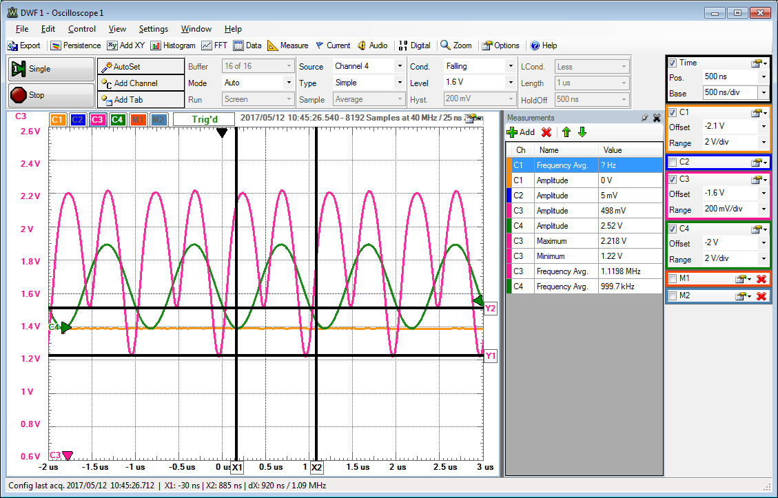
Folder 4 transistors:


fin100 kHz200 kHz500 kHz1 MHz1 MHz
Vin1.5 V
Vout0.25 V

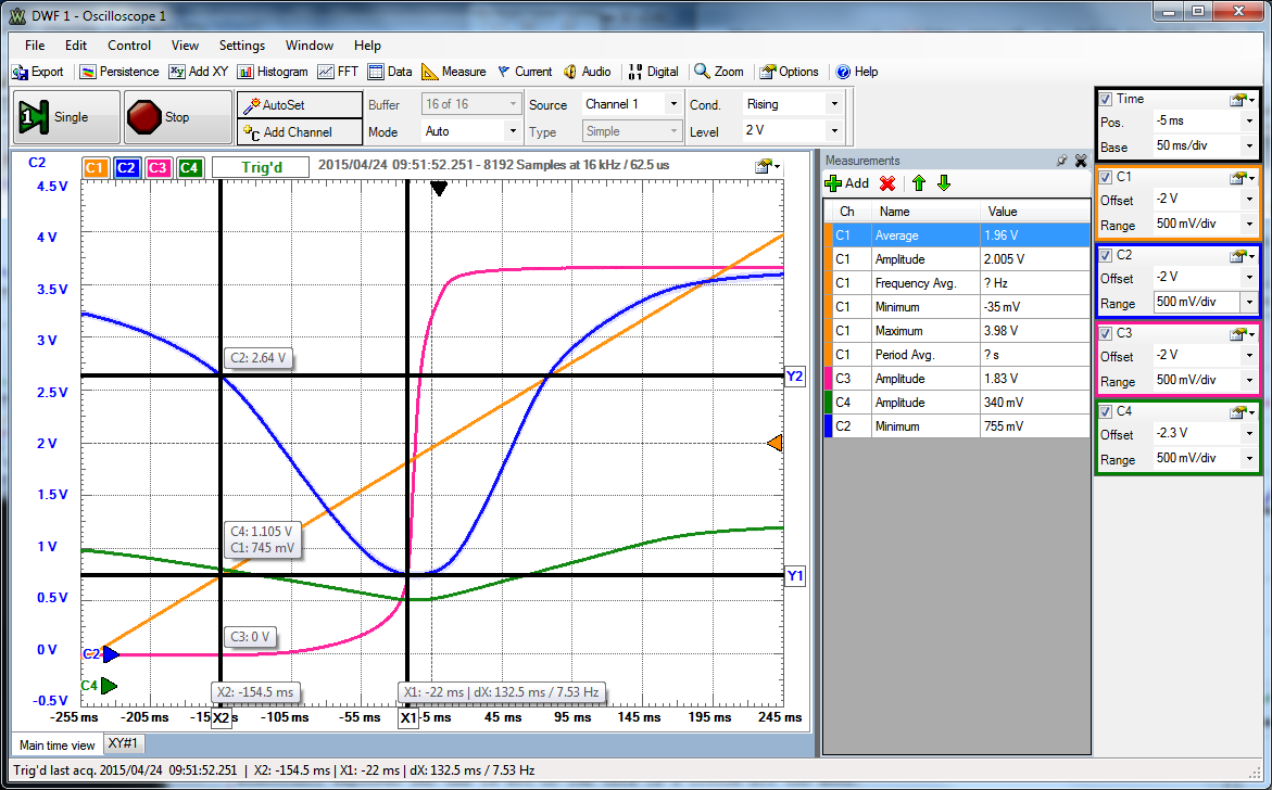
Vin 1.5 V amplitude gives at output 250 mV. At higher frequencies the midpoint low voltage at the output is different between rising and falling.
Difference of minimum: 500 kHz 230 mV, 100kHz 70mV, 10kHz 0 V.
Gain: 0.17

(simulation gain: 325 mV /1.5 V = 0.22)

Folder 3 transistors:


Vin 2.5V amplitude, 2.5 V offset, Vout 500 mV amplitude, 1.7 V offset, 10 kHz. No difference between rising and falling input signal for minimum voltage at the output.
Gain: 0.2
100 kHz Minimum difference for output with rising and falling input signal is 40 mV.
1 MHz gives 285 mV difference at the minimum.


( simulation gain: 0.6 V / 2.5 V = 0.24)


Supply voltage variations directly go into signal: gain = 1
Power supply rejection ratio is PSRR = 0 dB.