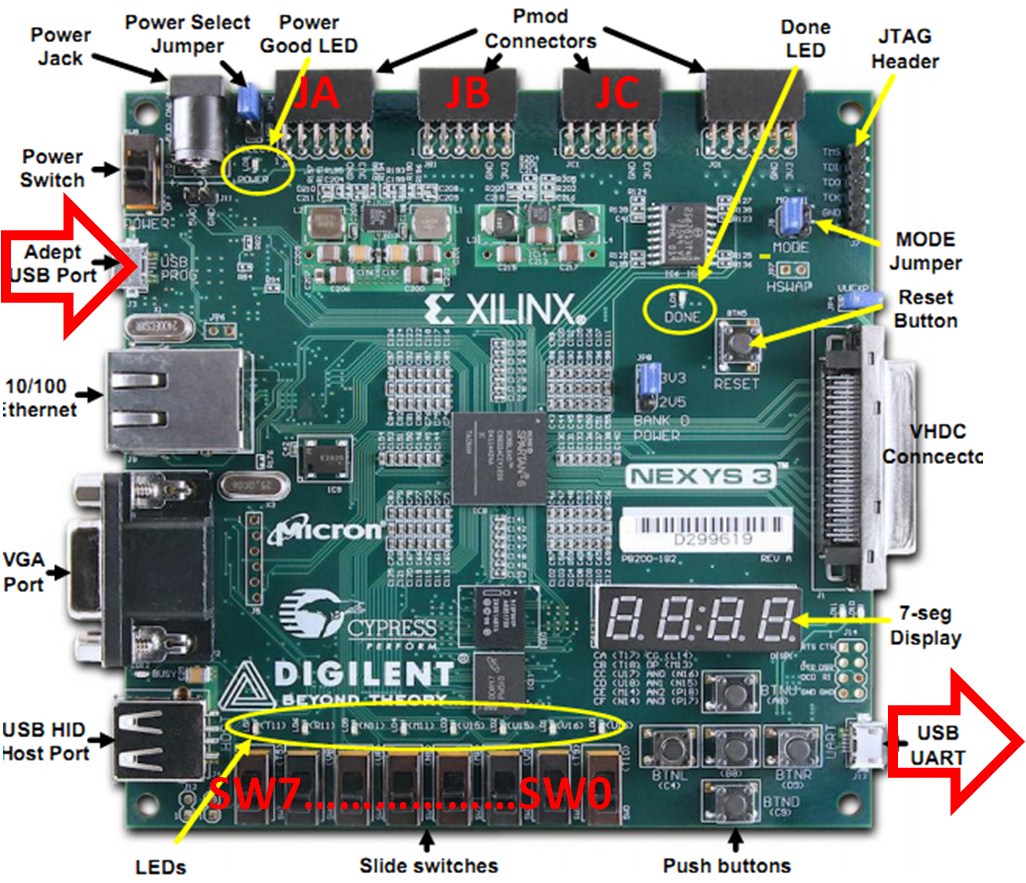
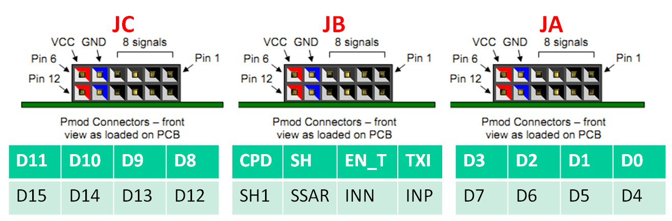
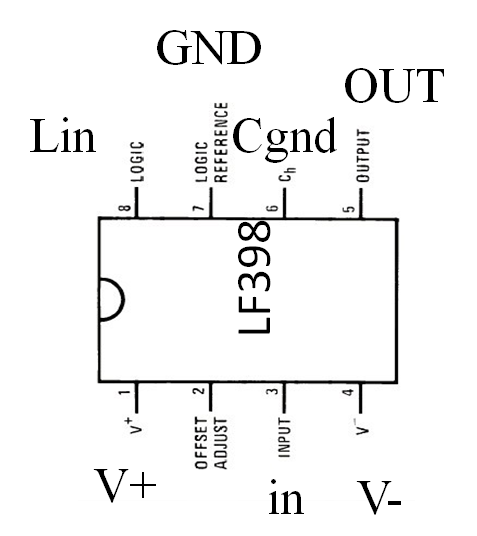
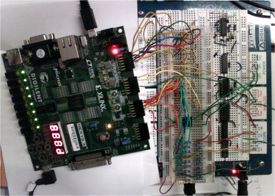
A Real Successive Approximation (SAR) ADC

List of parts


Electronic Explorer Board ($ 330 / $660)
Nexys 3 Board ($ 190 / $270)
1 LF398 (Sample and Hold)
54 Capacitors (C2C DAC)
Breadboard PCB like Electronic Explorer (EBay)

VHDL Files for Nexys 3 Board for Spartan 6, XC6SLX45, Package CSG324
Programming Bit File for Nexys 3 Board for Spartan 6, XC6SLX45, Package CSG324

Duration


6 Laboratories

Description


The system uses a NEXYS3 FPGA board as SAR controller, a C2C DAC, a LF398 as sample and hold, the Electronic Explorer to generate an input signal and measure signals with the oscilloscope.

Connect the DAC data inputs to the FPGA ports JA and JC. Start connecting the MSB pins of the DAC to the MSB data pins of the FPGA board. leave the remaining data ports open. Connect the ground from the FPGA, DAC and EE board.


CPD: compare data
SH:
EN_T:Enable signal due to switches
TXI: signal line UART
SH1:
SSAR: SAR operation finished
INN: Compare signal from output of DAC
INP: External Signal input

The output of the DAC is connected to the oscilloscope and the INN of the PMOD connector JB of the FPGA board. The INP of the JB connector of the FPGA port is the signal input for the ADC and is connected to AWG1 of the Electronic Explorer.
If the configuration of the FPGA board is not preconfigured, it can be loaded with the Adept tool, through the USB port at the upper left side.
L:/scripts/Vollrath/InEl/SAR/NEXYS3/SAR_C2C.bit
The switches on the lower left control the mode of operation:
The 7 segment display shows the result of the SAR conversion. A USB cable can be attached to the seriell USB port (red arrow, lower right FPGA board). Hyperterminal can be started with 38400 baud rate, 8 Databits, no parity and 1 stopbit, no flow control on the PC and connected to a COM port to transfer data from the FPGA board to the PC.

Sample and hold:


The analog input can be buffered with a sample and hold circuit (LF398). Power is supplied from VP = 5V and VN = -5V of the EE board. GND is connected to pin 7. A capacitance of C=pF is connected between pin 6 and GND. Lin is connected to the pin SH of connector JB to control sample or hold. The output of the sample and hold is connected to INP.

Check set up:

After connecting everything and turning power on generate a DC voltage between 0 and 1.6V (3.3V) with AWG1 as analog input signal. Measure with the oscilloscope signal SSAR(start of SAR conversion), SH,SH1, INN (DAC output voltage).
Since a capacitance based DAC is used, switch 1 should be on and the DAC generates normal and inverted data to eliminate problems with a DC voltage. This reduces the input range to half Vref:
Vrange = VRef/2=3.3V/2=1.65V.
The DAC will produce positive and negative pulses. Only during positive pulses the input signal is compared with the DAC signal.
The FPGA will always do 16 steps per conversion starting with the MSB. Depending on the switches different sample frequencies and number of bits are used.
Change sample frequency with the switches and verify correct operation with the oscilloscope.

Measure INL and DNL of the SAR

With a reasonable sampling frequency apply different input levels with AWG1 to the SAR and measure the transfer curve and calculate INL and DNL. The measurement can be manually done by reading the value from the 7 segment display or monitoring data via Hyperterminal (Histogramm test).

Implement and measure sample and hold circuit

Connect the IC LF398 between input signal and FPGA or DAC output and FPGA. Measure performance of the sample and hold circuit. Input signal, output signal and time behaviour. How much is switching noise?

Measure SNR of the SAR

Generate a sine wave with AWG1 and record the output data with Hyperterminal and do a FFT to determine signal to noise ratio and ENOB.

Final Questions

What are the performance limits of the investigated SAR? (Resolution, sample rate) How can the performance be improved?

Results