Sigma delta ( \( \Sigma \Delta \) ) analog to digital converter (ADC)


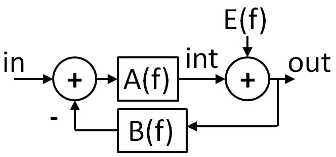
A \( \Sigma \Delta \) analog to digital converter (ADC) integrates (sigma) the difference (delta) between the input signal and an analog value generated by the current digital output code.
It is an oversampling ADC where the sample frequency \( f_{sampleIn} \)(clock frequency) is much higher than the bandwidth \( f_{bw} \) of interest.
The oversampling ratio OSR is defined as:
\( OSR = \frac{f_{sampleIn}}{f_{sampleOut}} \)
\( f_{bw} = \frac{f_{sampleOut}}{2} \)
A digital filter is used to downsample the digital output stream, increasing the number of bits and filtering out noise.
\( \Sigma \Delta \) ADCs can be of different order, active using operational amplifiers or switched capacitor circuits and passive.
There are also cascaded (MASH) \( \Sigma \Delta \) ADCs to prevent instability.

Objectives:
1. Provide high level no cost JavaScript models in this web page.
2. Provide working LTSPICE transistor level models for simulation.
3. Provide simple low cost analog circuits with FPGA data processing for real experiments and measurement.

First Order \( \Sigma \Delta \) ADC


A block diagram of a first order sigma delta ADC is shown here:

On the left the difference of V(in) and V(D) is integrated and then compared with V(CMP). The comparator operates with the clock frequency and gives for each clock cycle a new value.
A simple passive first order sigma delta converter uses resistors and capacitances.

The voltage V(INT n+1) at clock cycle n+1 is:

\( V_{int n+1} = V_{int n} + \frac{\delta t}{C} \left( \frac{ V_{not(Dout)} - V_{int n}}{R} + \frac{V_{in} - V_{int n}}{R} \right) \)
\( V_{int n+1} = V_{int n} + \frac{\delta t}{C \cdot R} \left( V_{not(Dout)} + V_{in} - 2 \cdot V_{int n} \right) \)

\( \delta t \) is the period of the clock.
\( V_{Dout} \) in a real logic circuit is 0V or VDD.

A current is charging the capacitance.
An active sigma delta converter limits the swing of V(INT):
\( V_{int n+1} = V_{int n} + \frac{\delta t}{C \cdot R} \left( V_{not(Dout)} + V_{in} - 2 \cdot V_{CMP} \right) \)
A passive sigma delta converter can limit the swing of Vint with a small \( \frac{\delta t}{C \cdot R} \) These equations are implemented in JavaScript for simulation on this website.


The general signal and noise transfer function can be calculated:

\( V_{out}(f) = \left( V_{in}(f) - B(f) V_{out}(f) \right) A(f) + E(f) \)
\( V_{out}(f) = V_{in}(f) A(f) - B(f) V_{out}(f) A(f) + E(f) \)
\( V_{out}(f) \left( 1 + B(f) A(f) \right) = V_{in}(f) A(f) + E(f) \)
\( V_{out}(f) = V_{in}(f) \frac{A(f)}{1 + B(f) A(f)} + E(f) \frac{1}{1 + B(f) A(f)} \)
For a passive first order sigma delta modulator:
\( \frac{v_{in} - v_{int}}{R} + \frac{-v_{out} - v_{int}}{R} = i_{int} \)
\( v_{in} - v_{int} - v_{out} - v_{int} = i_{int} R \)
\( v_{in} - v_{out} - 2 \cdot v_{int} = i_{int} R \)
\( v_{in} - v_{out} = i_{int} R + 2 \cdot v_{int}\)
\( i_{int} = v_{int} j \omega C \)
\( v_{int} = \frac{v_{in}-v_{out}}{j \omega C R + 2} \)
Comparing this with the general signal and noise transfer function gives:
\( B(f) = 1 \)
\( A(f) = \frac{1}{j \omega C R + 2} \)
\( V_{out}(f) = V_{in} \frac{1}{j \omega C R + 3} + E(f) \frac{j \omega C R + 2}{j \omega C R + 3} \)
\( V_{out}(f) = \frac{V_{in}}{C R} \frac{1}{j \omega + \frac{3}{R C}} + E(f) \frac{j \omega + \frac{2}{R C}}{j \omega + \frac{3}{R C}} \)

Bandwidth

\( \frac{1}{\delta t} = f_{CLK} \) is the sampling frequency.
The low pass corner frequency f3dB should be higher than \( \frac{f_{CLK}}{2 OSR} \lt f_{3dB} \) to prevent signal loss.
\( f_{3dB} = \frac{1}{2 \dot \pi C R} \leq \frac{f_{CLK}}{2} \) to limit aliasing from higher frequencies. The low pass corner frequency is even smaller for oversampling.
\( \frac{2 \pi}{2 OSR} \lt \frac{\delta t}{C \cdot R} \).
To prevent gain error from the signal transfer function
\( \frac{1}{| j \omega + 1 |} \gt (1 - 0.5 \frac{LSB}{V_{ref}} ) \)
\( \frac{1}{| j \omega + 1 |} \gt (1 - \frac{1}{2^{N+1}} ) \)
\( \frac{1}{\sqrt{ \omega^{2} + 1 }} \gt (1 - \frac{1}{2^{N+1}} ) \)
\( \frac{1}{(1 - \frac{1}{2^{N+1}} )^2} \gt \omega^{2} + 1 \)
\( \omega^{2} \lt \frac{1}{(1 - \frac{1}{2^{N+1}} )^2} - 1 \)
\( \omega^{2} \lt \frac{1 - 1 + \frac{1}{2^N}- \frac{1}{2^{2N+2}}}{(1 - \frac{1}{2^{N+1}} )^2} \)
\( \omega^{2} \lt \frac{\frac{1}{2^N} \left( 1 - \frac{1}{2^{N+2}} \right) }{(1 - \frac{1}{2^{N+1}} )^2} \approx \frac{1}{2^N} \)
\( \omega \lt \frac{1}{2^\frac{N}{2}} \)
Number of Bits fbw/fgRC OSR fgRC/fbw \( \frac{\delta t}{C \cdot R} > \)
1 0.88 1.5 1.1 3
4 0.25 6 3.9 2.1
8 0.065 38 16 1.33
12 0.015 240 64 0.835
16 0.0039 1521 256 0.53
20 0.00097 9660 1024 0.335
24 0.00024 61330 4096 0.21
\( f_{gRC} > 2^\frac{N}{2} f_{bw} = \frac{2^\frac{N}{2}}{2 \cdot OSR} f_{sample} \) Otherwise there is a gain error for fgRC.
\( \frac{\delta t}{C \cdot R} = \frac{2 \pi f_{gRC}}{ f_{sample}} \gt \pi \frac{2^{\frac{N}{2}} }{OSR} \)

Real circuit voltage limitations

The voltage V(INT) has to remain between VDD and 0 V and centers around \( V(CMP) = \frac{VDD}{2} \).
\( 0 \lt V_{CMP} + \frac{\delta t}{C \cdot R} \left( V_{not(Dout)} + V_{in} - 2 \cdot V_{CMP} \right) \lt VDD \)
\( 0 \lt \frac{V_{DD}}{2} + \frac{\delta t}{C \cdot R} \left( V_{not(Dout)} + V_{in} - V_{DD} \right) \lt VDD \)
mit \( V_{not(Dout)} + V_{in} = 0 \) or \( 2 \cdot VDD \)
\( \frac{\delta t}{C \cdot R} \lt \frac{1}{2} \)

Summary R, C limitations

The internal voltage level has to stay between 0 V and VDD.
\( \frac{\delta t}{C \cdot R} = \frac{1}{f_{sample} \cdot C \cdot R} \lt \frac{1}{2} \)
The input voltage swing for the comparator has to be above a certain minimum voltage \( \frac{V_{DD}}{gain} \).
\( v_{swing} = \frac{\delta t}{C \cdot R} V_{DD} > \frac{V_{DD}}{gain} \)
The input low pass corner frequency has to be larger than the bandwidth.
\( f_{bw} = \frac{1}{2 \pi C \cdot R} > \frac{f_{sample}}{2 OSR} \)

\( \frac{dt}{ C \cdot R} > \frac{2 \pi}{2 OSR} \)

Example of first order sigma delta ADC


Compare voltage V(CMP) = 0.5 V
Type of sigma delta converter:
Factor \( \frac{\delta t}{C \cdot R} \leq 1 \):
Input voltage V(IN) [V] from 0..1:

Simulate sigma delta ADC

Time 0
V(INT) 0.5
V(OUT) 0
V(D) 0

The resistors and the capacitor form a lowpass.
The corner frequency of the low pass should be greater than the bandwidth of interest.

Bitstream

The following table shows typical code sequences and transition voltages Vt from one code sequence to the next for a passive 1st order sigma delta modulator with different factors \( \frac{\delta t}{C \cdot R} \leq 1 \) of 0.2, 0.3, 0.1 affecting linearity.
Code Vt(0.2) [V] Vt(0.3) [V] Vt(0.1) [V]
00000000... 0 0 0
00010001... 0.097 0.04 0.17
001001001.. 0.183 0.11 0.27
01010101... 0.375 0.29 0.45
011011011.. 0.7 0.75 0.68
01110111... 0.84 0.91 0.79
11111111... 1 1 1
A DC input creates low frequency tones which can be in the band of interest. To increase the number of bits while reducing the data rate a digital filter can be used.

Digital Filter


The simplest filter is an averaging filter. For sigma delta converters sinc filters and downsampling are used.

A ramp of the input voltage can be used to analyze the bit stream.
In this example a sinc1, sinc2 and sinc3 filter can be applied for several oversampling rates [6].
The JavaScript filter code can be found in the source code (function gen_simRamp) of this page.
The Histogramm should have an average value of 20.
Pulse duty cycle: %
Overshoot: %

Filter type: Oversampling rate: Simulate ramp function and histogramm

A first order sigma delta converter gives a signal to noise ratio of:
\( SNR = 6.02 \cdot N + 1.76 - 20 log \frac{2 \pi R C f_s}{\sqrt{12}} + 30 \log OSR \) (0, Baker, 6.17)
For \( R C f_s = 1 \) this gives: \( SNR = 6.02 \cdot N + 1.76 - 5.17 + 30 \log OSR \)
For \( R C f_s = 4.4, \frac{1}{R C f_s} = 0.22 \) this gives: \( SNR = 6.02 \cdot N + 1.76 - 18.06 + 30 \log OSR \) (0, Baker, 6.18)
The increased resolution for oversampling is
\( N_{inc} = \frac{ 30 log OSR - 5.17}{6.02} \)
or
\( OSR = 10^\frac{N_{inc} \cdot 6.02 + 5.17}{30} \)

Doubling the oversampling rate OSR gives 1.48 more Bits:
\( N_{inc} = \frac{ 30 log 2}{6.02} = 1.48 \)

To realize this increased resolution the order of the sinc filter has to be one more than the order of the delta sigma modulator. (6, TI)

A Sinc2 filter has the following schematic with 2 integrators and 2 differentiators:

The width W of the registers has to be adjusted accordingly to the gain: (6, TI)
\( W = 1 + K \cdot log_2 OSR \)
K is the order of the filter.

Example:
16 Bit resolution needs SNR = 97 dB and gives OSR = 1521.
The width of registers has to be \( W = 1 + 2 \cdot log_2 1521 \rightarrow 23 \)

VHDL code for 24 bit wide 2nd order SINC2 filter. [6, Texas Instruments]


Bitsequence filter example

FFT spectrum

A FFT spectrum of an ADC shows the noise transfer function and signal to noise ratio.
1) FFT of 1 bit stream: Signal and noise transfer function
2) FFT of stream after decimation
The filter needs some time to initialize.
Calculate total power of noise and signal and compare FFTs.

Effect of bleeding can be seen with number of periods non integer.

An droop compensating FIR Filter [ http://www.cypress.com/file/123171/download ] with a function:
\( output(i) = \frac{-1}{K -2} input(i) + \frac{K}{K -2} input(i-1) + \frac{-1}{K -2} input(i-2) \)
can be activated.
This filter function can be implemented in an FPGA employing shift, add, subtract (using 2s complement) and multiply. Fractions are normalized with the word width of the signal. K values can be taken from the link above.
K values up to Fs/16 up to Fs/8 up to Fs/4
sinc1 25.6573 24.65659 21.04096
sinc1 error +/- dB 0.00017 0.0027 0.045
sinc2 13.79721 13.20875 11.12903
sinc2 error +/- dB 0.0004 0.0064 0.104
sinc3 9.843906 9.393567 7.835116
sinc3 error +/- dB 0.0007 0.011 0.177

Using a non prime number (40) as number of periods shows non random quantization noise distribution.
Setting the number of periods to 0 shows the transfer function of the filter.
Setting the number of periods to a negative value between -1 and 0 generates a DC value. Example: -0.615

FFT curve1: FFT curve2:
Number of periods (integer prime number): Possible values: 0, 3, 4.5, 7, 40, 43, 509, 1009, 1523, 1999
Oversampling rate:
Number of FFT points:
Bit width of filter:
Filter coefficient K:

Windowing for curve 1:


Simulate sine function into sigma delta ADC

Droop filter function

To investigate the transfer function levels at some frequencies are shown here in tabular form.
Select Number of periods: 0 to see the transfer function.
The transfer functio with FIR will show less droop at higher frequencies.

Results:


1st order passive sigma delta modulator FFT results.
SNR = 6.02 NBit dB + 1.76 dB + 30 · log(OSR)
Signal to noise ratio (SNR) in dB
OSR 30 log(OSR) dB SINC1 SINC2 SINC3 Number of pints FFT, register width W
4 18 11 17 18 Valid, FFT 1024, 16 Bit
8 27 17 25 27 Valid, FFT 1024, 16 Bit
32 45 29 40 42 Valid, FFT 1024, 16 Bit
256 72 47 63 64 Valid, FFT 1024, 30 Bit
512 81 53 71 72 Valid, FFT 1024, 30 Bit
2048 99 65 86 87 Valid, FFT 1024, 40 Bit
FFT 256k, Bit width 30, oversampling 32, Duration 2 min
FFT 256k, Bit width 30, oversampling 512, Duration 7 min
FFT 1M, Bit width 30, oversampling 512, Duration 27 min

An OSR = 256 can give 10 Bit.
An FPGA running at 100 MHz can sample 44kHz audio and gives an OSR = 2048 and 14 Bit with a 1st order sigma delta modulator and a sinc2 filter.

Table with required register width W = 1 + K log2 OSR for different OSRs and sinc filters.
OSR SINC1 SINC2 SINC3
4 3 5 7
8 4 7 10
32 6 11 16
256 9 17 25
512 10 19 28
2048 12 23 34
16k 15 29 43

Summary

The influence of the R and C of a first order sigma delta converter for correct functionality to avoid saturation at the input of the integrator can be studied.

Digital sinc filters are presented in VHDL code and as simulation.
A ramp test giving a histogram for these filters can be generated showing big errors.
Typical output bit sequences are presented before and after filtering and decimation.
Spectral test varying filter width, FFT points and filters can be studied.
Usage of non integer number of periods show bleeding in the FFT.
Limitations of small filter width and influence of filter on the transfer characteristics can be seen.
Droop of the sinc filter has to be compensated by an additional FIR filter or is limiting the usable bandwidth.

An FPGA running at 100 MHz can sample 44kHz audio and gives an OSR = 2048 and 14 Bit with a 1st order sigma delta modulator and a sinc2 filter.
Doubling the oversampling rate OSR can give 1.48 more Bits.

References


[0] CMOS Mixed-Signal Circuit Design, R. Jacob Baker "http://cmosedu.com/cmos2/book2.htm"
[1] Analog Devices Sigma Delta converter simulation "http://www.analog.com/en/design-center/interactive-design-tools/sigma-delta-adc-tutorial.html"
[2] Demystifying Delta-Sigma ADCs "https://www.maximintegrated.com/en/app-notes/index.mvp/id/1870"
[3] Wikipedia Delta-sigma modulation https://en.wikipedia.org/wiki/Delta-sigma_modulation
[4] Texas Instruments http://www.ti.com/lit/an/slyt423/slyt423.pdf
[5] Nuts and Bolts of the Delta-Sigma Converter, Texas Instruments, https://www.youtube.com/watch?v=oVti3b4rqQA
[6] Combining the ADS1202 with an FPGA Digital Filter for Current Measurement in Motor Control Applications, Texas Instruments, VHDL code
[7] Wikipedia Window function
Window function - Wikipedia