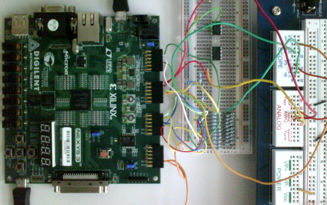
 Figure: Physical test setup with 10 bit R2R DAC
What resolution does the sine DAC have?
switch(2..0) = 000; tCLKD = 40 ns; fCLKD = 25 MHz
Effective number of bits ENOB:
\( SNR = 6.02 \cdot N_{Bit} + 1.76 - 5.17 + 30 log OSR \)
An oversampling of 2048 should give an increase in SNR of \( 30 log OSR \approx 95 dB \).
Since the sigma delta modulator has a 1 bit output NBit = 1.
ENOB:
\( ENOB = \frac{95 - 5.17 +1.76 }{6.02} \approx 15 \)
Bandwidth:
OSR · tCLKD = 2048 · 40 ns = 80 μ s gives one data point.
For fbw 2 points are needed.
\( f_{bw} = \frac{1}{2 \cdot 80 \mu s} = 6.25kHz \)
Minimum input signal frequency:
One period in 16k points.
\( f_{sig,min} = \frac{1}{16 \cdot 1024 \cdot 80 \mu s} = 0.763 Hz \)
Time for getting 16k data, one periodof sine signal:
\( T = \frac{1}{f_{sig,min}} = 1.31 s \)
Measurement of the sine signal period for sw(6,5)=00; sw(4,3)=11.
16k points sine lookup table or oscilloscope measurement confirms 16k points.
10 Bit DAC means 10..16 points per code.
For FFT use 43 periods to get peak at higher frequency.
RC dimension:
\( \delta t = 40 ns \)
12 Bits to have lowest fgRC = 64 fbw = 400 kHz
\( R C = \frac{1}{2 \cdot \pi \cdot 400 kHz} = 397 ns \)
Sample and Hold C requirement for 12 Bit, 3.3V -> C > 80 fF
For example: R = 10 k Ω C = 10 pF
R C = 100 ns
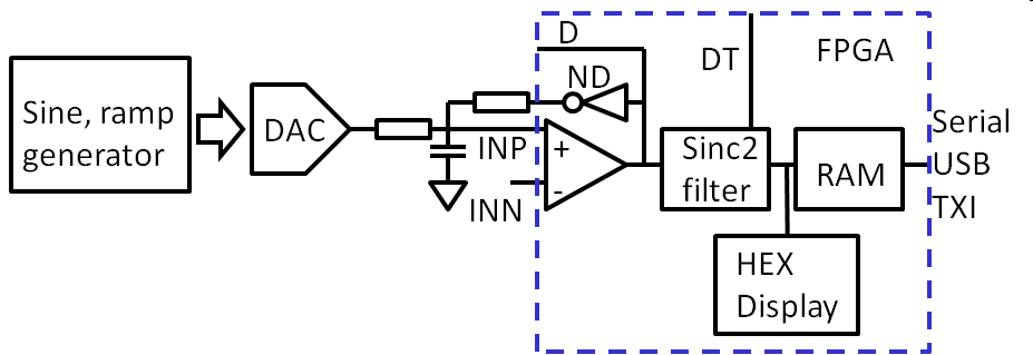
Data processing
The ADC data received by the serial interface of the PC.
Identify and copy a 16k block in the log file.
Transfer hex values to decimal values.
For a ramp or sawtooth signal identify one period and extract the values for a histogramm evaluation.
For a sine signal confirm a prime integer number of cycles or apply a windowing function for FFT.
Do the FFT and calculate signal to noise values.
The ADC data received by the serial interface of the PC is analysed using FFT Javascript
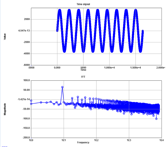
Signal level is 65.19 dB and the total noise 18.07 dB.
This gives SNR = 47.12 dB, which is ENOB = SNR / 6.07 dB = 7. 76 Bits.
The distortion with harmonics can be seen in the spectrum, coming from non linearities.
Not taking into account distortions a total noise magnitude of 8.82 dB can be seen.
This gives SNR = 56.63 dB, which is ENOB = SNR / 6.07 dB = 9. 28 Bits.
Unfortunately quality of sine signal is not given.
Electronic Explorer has a 10-bit DAC. R2R DAC with 0.1% resistance can also give 10-bit.
Probably signal to noise is limited by the quality of the DAC.
Diagnosis of a sigma delta ADC
If the theoretical SNR is not reached a diagnosis is needed.
Clock jitter
Clock jitter will show up using test signals of various frequencies.
With clock jitter the noise will increase with higher frequency test signals, since dV/dt will be bigger and consequently the error will be bigger at higher frequencies.
Inter symbol interference
Inter symbol interference changing the digital output waveform depending on the output code pattern can be studied with varying sample rates. Lower sample rates and clock frequencies should give less inter symbol interference noise.
Signal and power supply noise
Signal and power supply noise is caused by external signal sources and can show up as harmonics or random noise. Shielding and buffer capacitances can be used to lower ths noise. With active sigma delta modulators the input range can be increased with higher power supply voltages. If the SNR is increasing with high power supply voltages shielding und buffer capacitances are not sufficient.
Varying oversampling rate
Higher oversampling rate should give more bits ENOB and SNR.
Summary
16 bit digital code output for sawtooth, sine