Analyzation of the ADC DAC test simulation with a ramp signal input - 600K
ADC DAC test simulation with a ramp signal in LTSPICE - 600K
For creating our data to analzye we need to run a simulation in the Programm 'LTSPICE'.
Therefore we load the prepared .asc-files in LTSPICE.
Before we can start the analysis
we need to change the input signal from a sine wave to a ramp signal. To do that we just
comment out the sine wave as the input and define the ramp signal as the new one.
After specifying the duration of the simulation with 655.36 us we also need to change the
data we want to save. In this simulation we are only interested in the output voltage.
After all this preparations we are ready to start the simulation. The picture underneath
displays the result of the simulation.
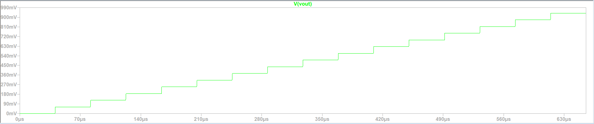
Waveform output with a ramp signal input in a ADC DAC simulation.
Extracting and filtering the values - 600K
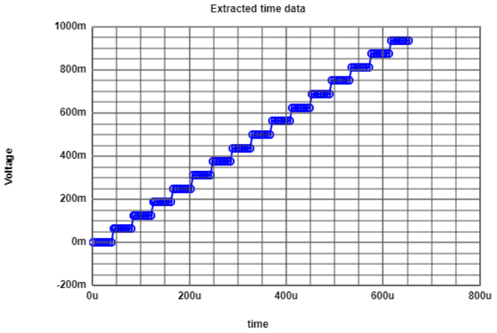
Out of our generated transfer curve we can do different anayses. At first we start with the DAC characteristics.
Therefore we only look at the different output voltage levels.
As we can see we have 16 of them over a the whole time duration of 655.36 us.
Before we started the simulation in LTSPICE we specified that the output voltage should be saved.
For the analyzation of the DAC characteristics we use the javascript tool Read Raw File.
This tool will help us to filter the data of the simulation. LTSPICE gave us a total of 3328663 measurement points. For the analysis of the DAC we only need one point at each of the 16 voltage levels. LTSPICE gave us a total of 3328663 measurement points.
To do the filtering we need to give the 'Read Raw File'-Tool some further information.
We have to enter the total duration of the simulation (start and stop time) and the step size of the desired points.
Because we need only 16 points we have to devide the total time of 655.36 us by 16. By doing that we receive a stepsize of 40.96 us.
Input values for the 'Read Raw File'-Tool:
- Start time: 0
- Stop time: 655.36E-6
- Time step: 40.96E-6
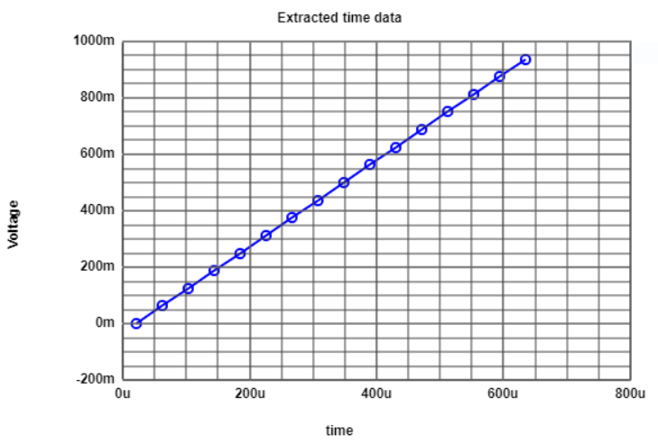
Filtered curve showing the voltage in mV over time in us. |
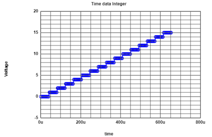
Map extracted values to integer - 600K
The javascript tool 'Read Raw File' also gives us the posibility to map the voltage to a code. Therefore we need to specify the number of the highest code which is 15 (range is from 0 to 15). After clicking on the 'Map to integer' button the tool shows us the desired graph which should look similar to the one before.
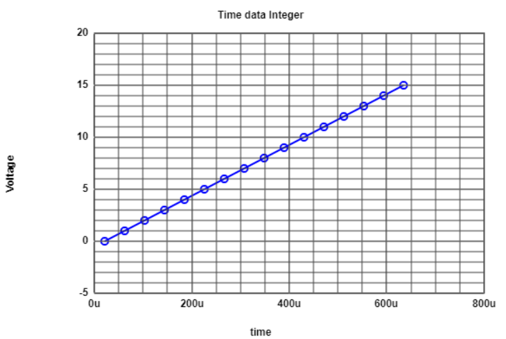
Filtered curve mapped to integer from 0 to 15.
Analyzing the DAC INL and DNL error - 600K
Mapping the values to integer is not the only avaible process we can do with the data.
Cause of examinating the DLC characteristics we also want to check the INL and DNL error.
The results are shown in the graphs underneath.
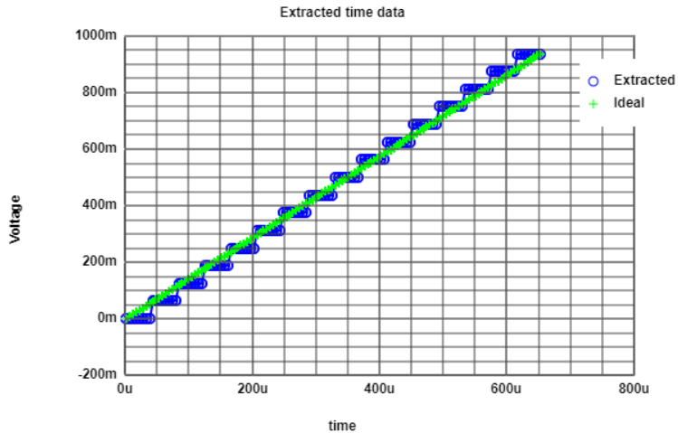
The left graph displays the ideal and real curve. As expected the ideal and real curve are the same.
We did an ideal simulation of an ADC DAC circuit with an ideal input signal.
We also calculated the filter exactly to get the measurement points at the beginning at each voltage level.
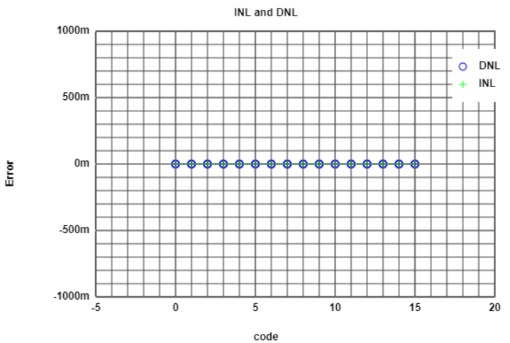
Our INL and DNL is also zero at every number of code.
On the next slide are the exact values of each code presented with the calculated INL and DNL errors.
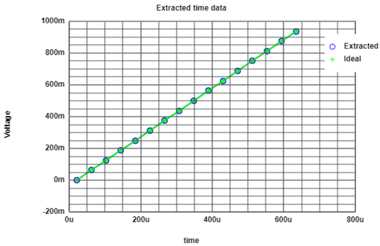
Ideal and real curve of the DAC characteristics |
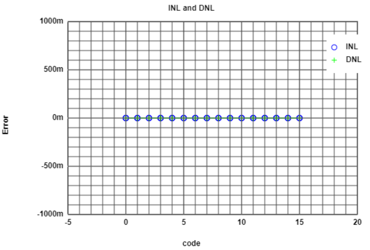
INL and DNL error graph of the DAC characteristics. |
ADC analyzation with an histogram test - 600K
To do the histogram test on our data we need to change the filter values. For examinating the DAC characteristics we only wanted one
measurement point per voltage level. For the histogram test this will not be enough. We will rise the amount of points per level by 8.
The previous filter values for the start and stop time will remain the same. We only going to edit the time step. Previously we had a
time step size of 40.96 us. To get 8 points we need to devide that by eight. The new time step will be 5.12 us.
The right graph shows the extracted values with the voltage in mV over the time in us.
The right one displays the extracted values mapped to integer (range from 0 to 15).
Due to the fact that we are still dealing with an ideal curve we will not see any differences in the step size of the voltage levels.
A table of the values will not be shown. With 8 points per level 128 points are to much to display it in this report.
Input values for the 'Read Raw File'-Tool:
- Start time: 0
- Stop time: 655.36E-6
- Time step: 5.12E-6
Extracted values with 8 points per voltage level. |
Extracted values with 8 points per voltage level mapped to integer. |
ADC analyzation with an histogram test part 2 - 600K
With filter attributs of more than one value per voltage level it's not useful to do an DAC INL and DNL analyses. For each level we will always have at least 7 points with an error. This is proven by the graph on the right side.
Ideal and real curve with 8 points per voltage level. |
DAC INL and DNL error with 8 points per voltage level mapped to integer. |
ADC analyzation with an histogram test part 3 - 600K
We have exactly 8 measurement points at each level with the same level of voltage at each group of 8.
From level to level the increase of voltage is always the LSB of 0.0625 V. Without even calculating it we can say the DNL error is 0.
Due to the fact that \(INL(code) = \sum_{i=0}^{code}DNL(i)\) the INL error is also 0 for all levels.
INL and DNL by using a histogram test.
Analyzation of the ADC DAC test simulation with a sine signal input - 600K
ADC DAC test simulation with a ramp signal in LTSPICE - 600K
We start the ADC DAC test simulation again. This time we change the input from a ramp signal to a sine signal.
The time duration is still set to 655.36 us.
Waveform of the ADC DAC test simulation with a sine signal input.
Extracting the values and mapping it to integer - 600K
After the simulation is done we again use the 'Read Raw File'-Tool to extract our data.
The filter values will remain the same:
- Start time: 0
- Stop time: 655.36E-6
- Time step: 5.12E-6
For receiving the amount of voltage levels we simply count the points shown in the left graph. To be really sure we could also check the list of extracted values with 128 measurement points. The examination will tell us that we again have 16 different voltage levels. With that knowledge we again can map the values to integer. The result is shown in the right graph.
Extracted values of the ADC DAC test simulation with a sine signal input. |
Extracted values mapped to integer. |
Histogram test on the sine signal in the 'Read Raw File'-Tool - 600K
After the simulation is done we again use the 'Read Raw File'-Tool to extract our data.
Histogram test (INL and DNL) on the simulated sine signal.
FFT analyses of the sine signal - 600K
Despite of the 'Read Raw File'-Tool there is also a tool provided for a FFT analyses. As input we use the extracted values mapped to integer out of the 'Read Raw File'-Tool. After reading in the values and generating the charts the tool puts out the following informations. On the left side we can see a table signal to noise ratios. The same information is also displayed in a graph (right side).
FFT analyses. |
INL and DNL error out of the FFT analyses - 600K
After specifing the number of bits to 4 we get the real INL and DNL error. The FFT-Tool will compare the simulated sine signal with an ideal one.
The tool also displays us the following:
- INLmax: 0.33
- INLmin: -0.25
- DNLmax: 0.5
- DNLmin: -0.5
INL and DNL error out of the FFT analyses.
Simulation R2R DAC - 419L
Introduction
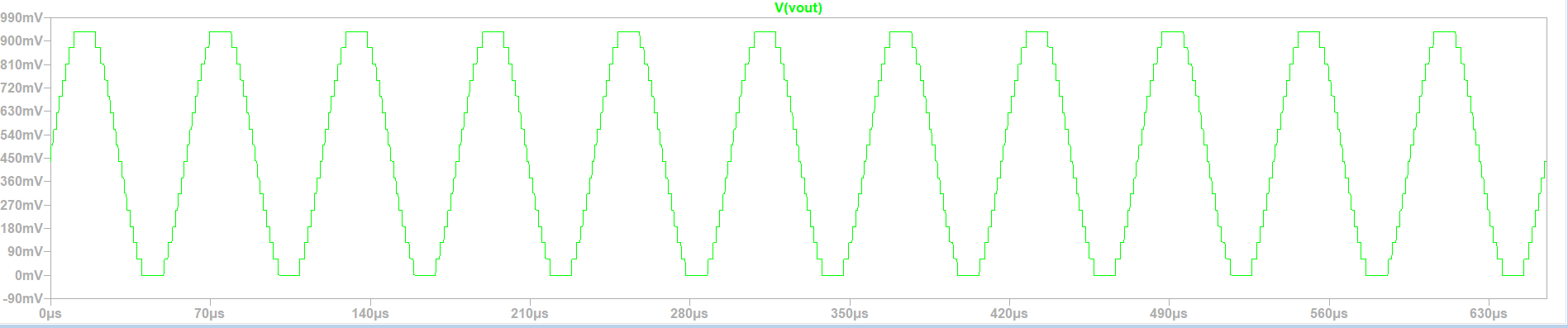
In this part of of the laboratory a 4-Bit R2R DAC is used. Therefore the digital output of the ADC are connected to the different positions at the DAC input. The input signal is a ramp.
LTspice schematics R2R DAC
LTspice Output measurement R2R DAC
The quantization is clearly visible in the picture. The first step of the ramp represents the signal 0000, the next step 0001 up to 1111. D0 changes Vout from 0 to Vdd/2^n (n number of bits). In our case the influence of D0 is 0.0625V. D1 influences the output voltage with the value of Vdd/2^(n-1). In the end the voltages are added up at the output voltage.
Simulation R2R DAC - 419L
Non ideal R2R DAC
Now we change the resistance of R6 and R9. This leads to a change of the behavoir of the whole resistor system. In an ideal R2R DAC there is an constant structure. Between the node and the digital input is a resistor with double the value of the resistance between the nodes. Now a higher jump of the voltage occures when D3 is switched from GND to VDD. The systematic increase with the same stepsize is destroyed.
Simulation R2R DAC - 419L
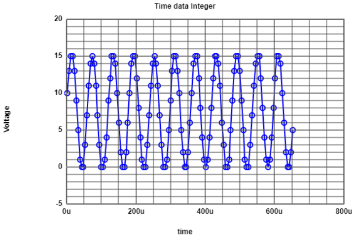
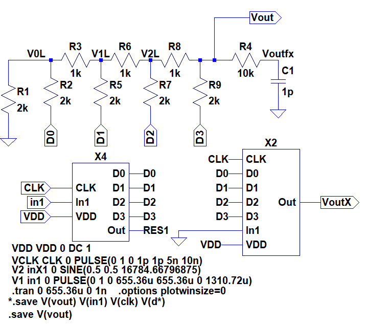
Non ideal R2R DAC - time data
To perform the DNL and INL analyse the raw data is uploaded to the webpage. Again only 16 points are used for the calculation. At a real system an digital code is applied on the inputs of the DAC and the output voltage is measured with a multimeter. A average filter is recommended at the output to filter noise. The other steps are similar to the simulation.
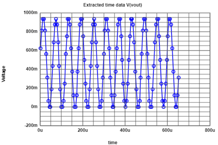
Extracted time data
A non linear behavoir occurs because of the changes of the resistor values.
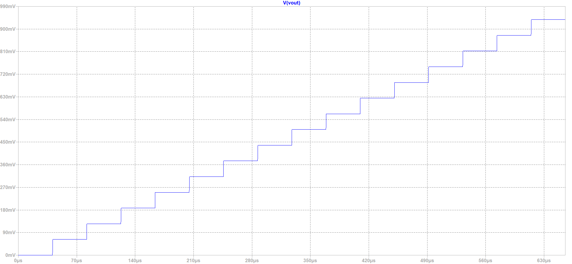
Time data integer
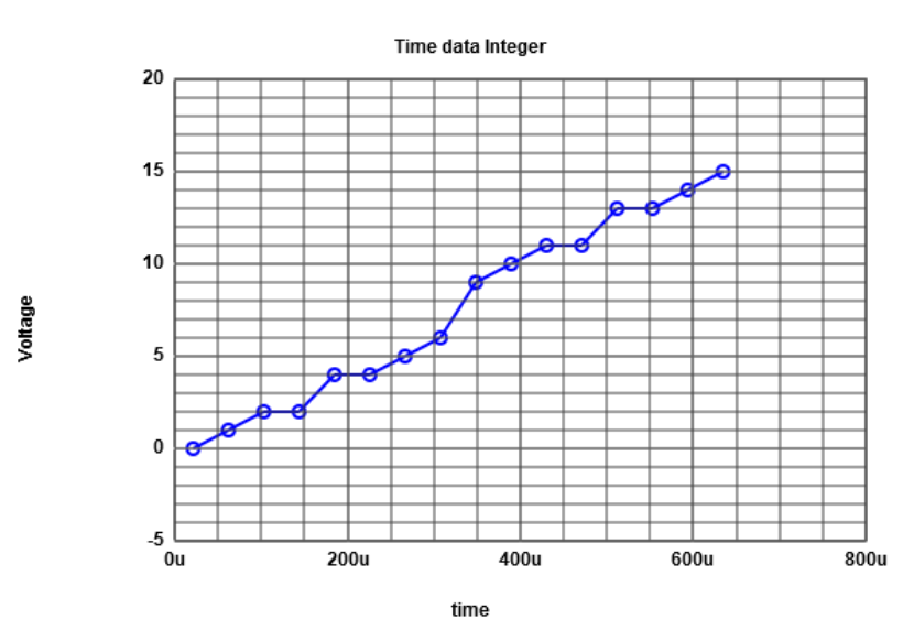
A look at around 175us shows a jump of the voltage from 2V to 4V. Before and after the jump the voltage stays the same. At around 500us the same behavoir occurs again. At timestep 325us a jump of 4V is measured. At this timestep the D3 input changes his value for the first time. Because of the change of the resistances only 12 different voltage values at the time data scale are possible to generate.
Simulation R2R DAC - 419L
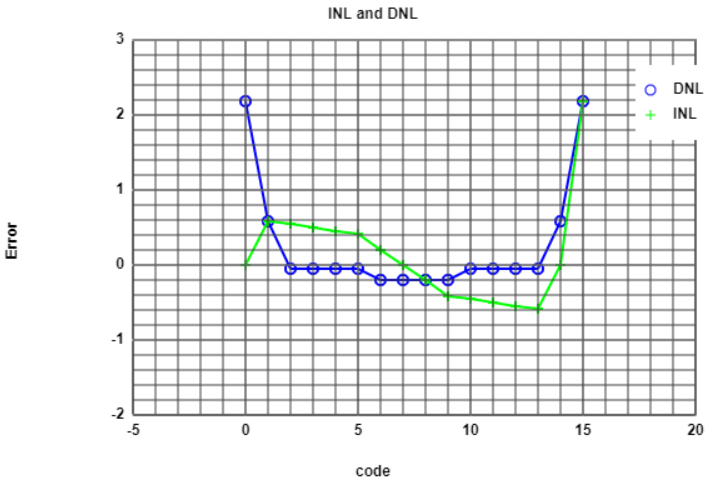
Non ideal R2R DAC - DNL and INL
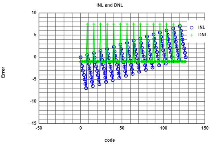
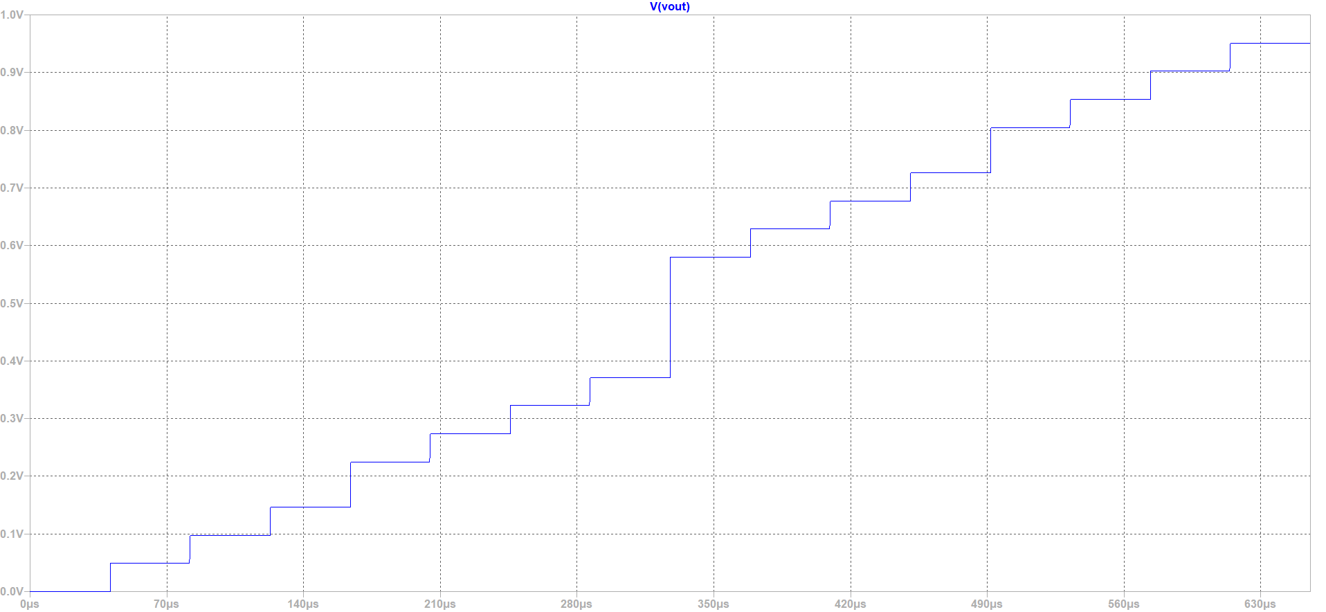
Extracted time data with ideal curve and DNL INL result on the right
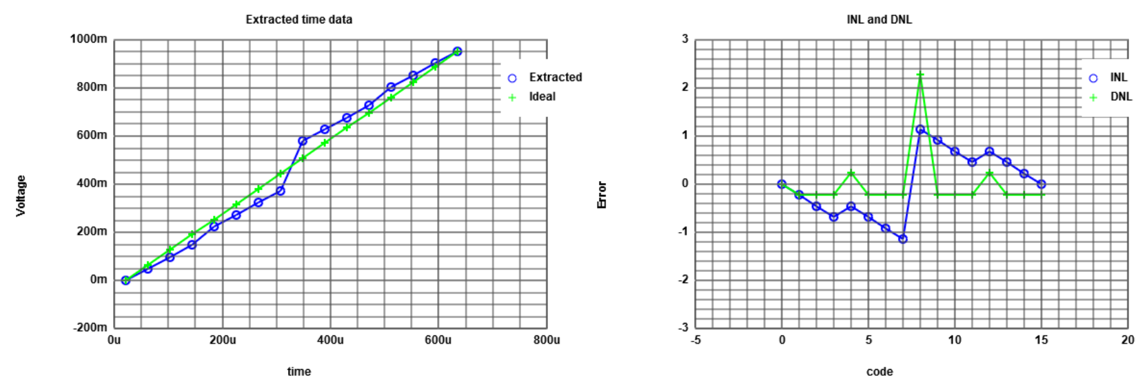
The difference between ideal curve and measured curve is clearly visible. At the beginning the measurment results are lower thann the ideal curve. A DNL bigger than 1 is an indicator of a non-monotonic tranfser function of the DAC. This could lead to stability problems of a closed-loop system.
| Code | 0000 | 0001 | 0010 | 0011 | 0100 | 0101 | 0110 | 0111 | 1000 | 1001 | 1010 | 1011 | 1100 | 1101 | 1110 | 1111 |
| VoutIdeal[mV] | 0 | 62.5 | 125 | 187.5 | 250 | 312.5 | 375 | 437.5 | 500 | 562.5 | 625 | 687.5 | 750 | 812.5 | 875 | 937.5 |
| Vout[mV] | 0 | 48.85 | 97.71 | 146.57 | 224.75 | 273.61 | 322.47 | 371.33 | 579.80 | 628.66 | 677.52 | 726.38 | 804.56 | 853.42 | 902.28 | 951.14 |
| INL | 0 | -0.22 | -0.44 | td>-0.65 | -0.40 | -0.62 | -0.68 | -1.06 | 1.28 | 1.06 | 0.84 | 0.62 | 0.87 | 0.65 | 0.43 | 0.21 |
| DNL | - | -0.28 | -0.28 | td>-0.28 | 0.15 | -0.28 | -0.13 | -0.43 | 2.06 | -0.28 | -0.28 | -0.28 | 0.15 | -0.28 | -0.28 | -0.28 |
With this table it is possible to calculate the DNL and INL. The results are shown in the picture above.
Simulation sinus on R2R DAC - 419L
sinus R2R DAC -
Now a sinus is set to the input of the non ideal R2R DAC
Extracted time data
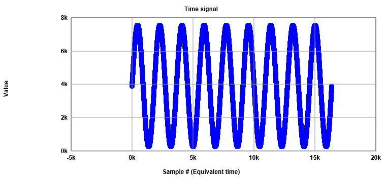
The sine signal is clearly visible.The jump of the voltage caused by the resistor change is not visible anymore. The following analyse of the measured signal shows the jump again.(look at histogram)
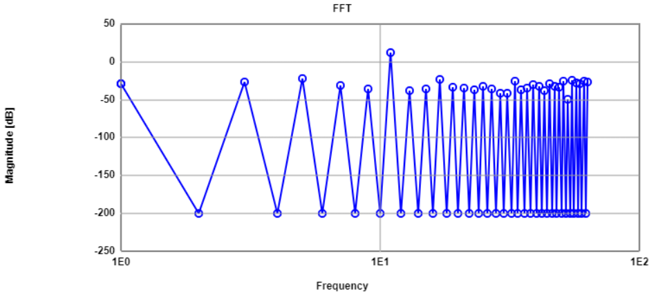
FFT
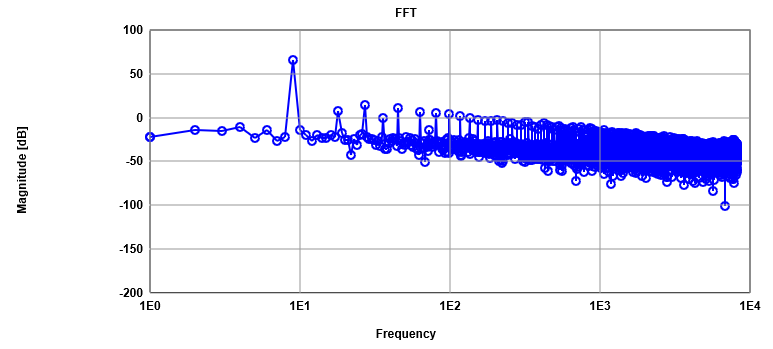
The fast fourier transformation shows an decrease in magnitude for higher frequencies. There is one point at around 9Hz which indicates a very high magnitude. The system has an low pass filter behavoir, shown with the decrease of the magnitude for high frequencies.
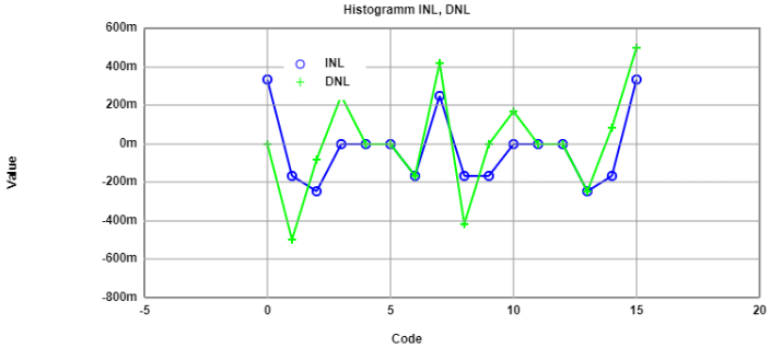
Histogram
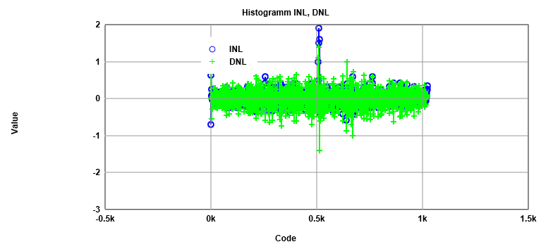
The histogram test shows also an DNL value of higher than 1 for the DAC which was already decribed before. It is recommended to have a INL and DNL in the range of +- 0.5LSB. This can be achived by reducing the number of bits. But the output accuricy will be reduced too. The result the code range is not from the power of 2.
Sometimes reordering of the codes solves the problem, if the LSB is big and a clear difference between the codes occures.
This process is called digital calibration.