Simulation and analysis of a ramp signal: DNL, INL, LSB
Simulation and analysis of a sine signal: FFT, DNL, INL, SNR
Summary
This is a laboratory to simulate an ADC DAC set up with ramp and sine test.
ADC DAC Schematic
The schematic shows a 4-bit ADC DAC simulation set up.
Simulate a ramp test
V2 in1 0 PULSE()
Make sure the .save V(in1) V(vout) saves vout as last value, to be able to postprocess it.
The simulation generates a file 4Bit_ADC_DAC_pipe.raw with simulated values.
Unfortunately this file is binary coded and timesteps are varying.
Extract the simulated values with
Read Raw File .
You can also calculate INL, DNL with any tool you like.
Document and discuss INL and DNL values.
Simulate a sine signal test.
Extract the simulated values with
Read Raw File .
Calculate FFT, INL, DNL with
FFT webpage and paste the
extracted values from LTSPICE into the input field.
Document and discuss FFT, INL, DNL and SNR values.
Please submit via email to joerg.vollrath@hs-kempten.de until 30.10.2019 a zipped
file of your group directory with your web report covering laboratories 1..3.
Addendum 31.10.2019
Please remove in LTSPICE folder the simulation output files .raw.
In LTSPICE select a different folder for the output files:
LTSPICE Tools, Control Panel, Waveforms, Store .raw in a special directory, C:\var\raw
You should zip the folder with a name like: 2019_Group<A..P>0<0,1>
Video Instructions LTSPICE ADC DAC Test Circuit
This video presents the download and run of LTSPICE files.
Search for "Vollrath InEl"
Open LTSPICE presentation.
Go to "Scalable behavioral 4 Bit DAC",
"Scalable behavioral 4 Bit ADC",
"Test for 4 Bit ADC and DAC" slides and download circuits (.asc) and (.asy)
presented to you after clicking on the circuit.
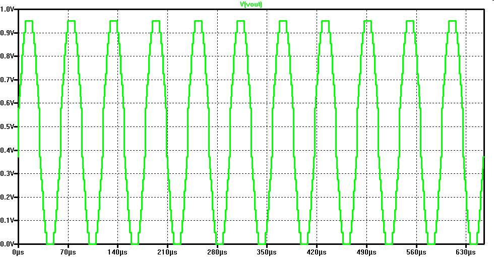
Run the sine simulation and view V(in1),V(out).
Create a pulse voltage source:
V1 in1 0 PULSE(0 1 0 655.36u 655.36u 0 1310.72u)
Run a ramp simulation.
Duration 10:52 min
LTSPICE Ramp simulation of ideal ADC DAC Test Circuit
11:30
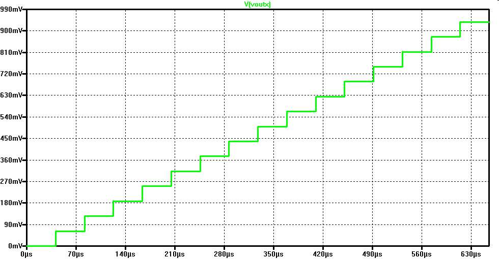
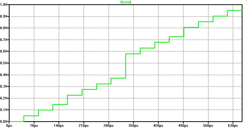
The ramp is generated with the source V1 and a pulse.
The pulse has a rise time of 655360ns.
The clock is sampling with 160ns.
This gives 4096 values.
The 16 steps of the 4 bit test circuit can be seen.
The output range is from 0V..0.937V.
Video Instructions LTSPICE INL, DNL FFT Analysis
This video presents the analysis of LTSPICE simulation files.
Run the ADC DAC test simulation in LTSPICE with a ramp.
Extract the simulated values with
Read Raw File .
Use analysis buttons to:
Show extracted values
Map values to integers
DAC INL, DNL analysis
ADC histogram analysis
Run the ADC DAC test simulation in LTSPICE with a sine signal.
Extract the simulated values with
Read Raw File .
Use the integer values for a FFT analysis.
Duration 13:48 min
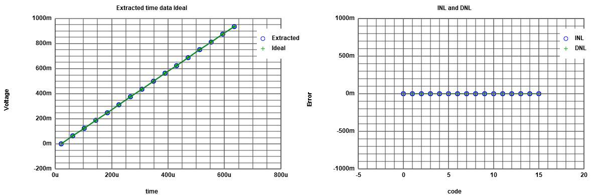
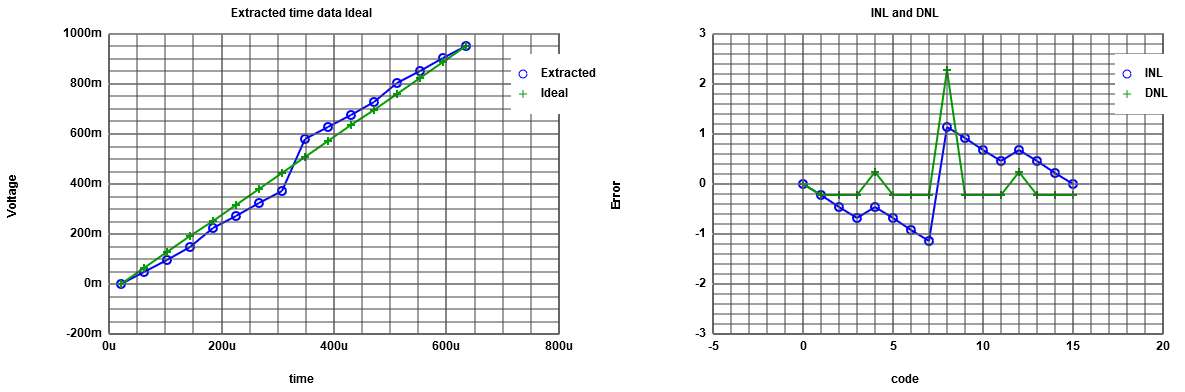
LTSPICE ramp INL, DNL Analysis
For LTSPICE raw file reading start time is 0, Stop time is 650us and time step is
655360/16 ns = 40960 ns = 40.96us
This gives 16 values.
Map to integer scale is set to 15 and DAC INL, DNL analysis gives optimum values of 0.
11:50
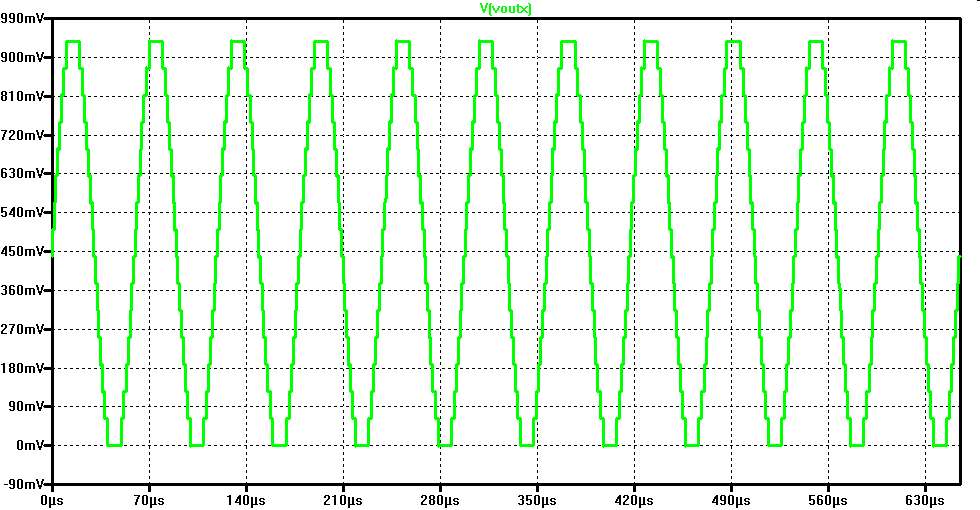
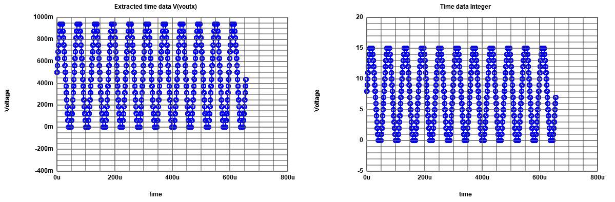
LTSPICE sine preparation for FFT Analysis
11:51
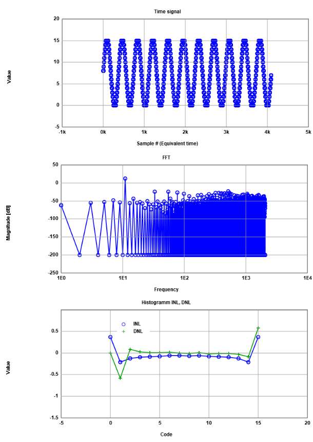
The simulation gives exactly 11 periods of the signal.
For LTSPICE raw file reading start time is 0, Stop time is 655.3us and time step is 160ns.
Mapping is done to a range of integer up to 15.
LTSPICE sine FFT Analysis
The FFT analysis is done with 4 Bits and 4096 points.
Signal magnitude for frequency 11 gives 11.9 dB.
Total noise gives -13.7 dB.
First harmonic at 517 is -23.08 dB.
So total noise is limiting signal to noise ratio and gives ENOB = (11.9-(-13.7)-1.76)/6.02 = 3.96 bits.
12:06
Simulation R2R DAC
The schematic shows a 4-bit R2R DAC.
We will use it in the ADC DAC simulation to see some errors.
Create a symbol and hook it up to the ADC DAC test circuit from last week.
Modify the resistance values. For example 1.5k, 2.5k, 1.3k, 1.7k.
See first LTSPICE schematuc for used values.
Simulate a ramp test.
Extract the simulated values with
Read Raw File .
Calculate INL, DNL with any tool.
Document and discuss INL and DNL values.
Simulate a sine signal test.
Extract the simulated values with
Read Raw File .
Calculate FFT, INL, DNL with
FFT webpage and paste the
extracted values from LTSPICE into the input field.
Document and discuss FFT, INL, DNL and SNR values.
Duration 6:34 min
LTSPICE Ramp simulation of real ADC DAC Test Circuit
12:08
R9 for the most significant bit is changed to 1.5k.
R6 for the second most significant bit is changed to 1.3k.
A big step in the output can be seen.
For LTSPICE raw file reading start time is 0, Stop time is 650us and time step is
655360/16 ns = 40960 ns = 40.96us
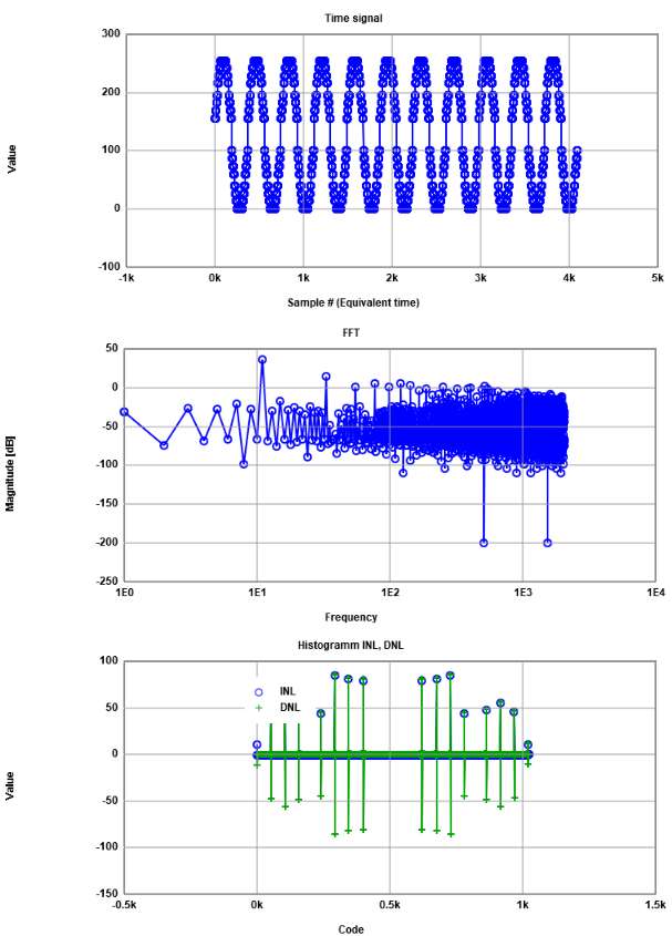
INL and DNL are well out of range of 1/2LSB.
The center peak in DNL is caused by R9.
The smaller peaks are caused by R6.
This behaviour is typical for a binary architecture.
Errors in the lower bits will show up with less impact to overall INL and DNL.
12:19
LTSPICE sine simulation of real ADC DAC Test Circuit
12:19
R9 for the most significant bit is changed to 1.5k.
R6 for the second most significant bit is changed to 1.3k.
FFT of LTSPICE sine simulation of real ADC DAC Test Circuit
For LTSPICE raw file reading start time is 0, Stop time is 655.3us and time step is 160ns
Map to integer range is 255.
Signal level (11): 36.85 dB.
Total noise: 17.44 dB.
First harmonic (33): 14.76 dB.
ENOB = (36.85 - 17.44 -1.76)/6.02 = 2.93 bits.
12:50
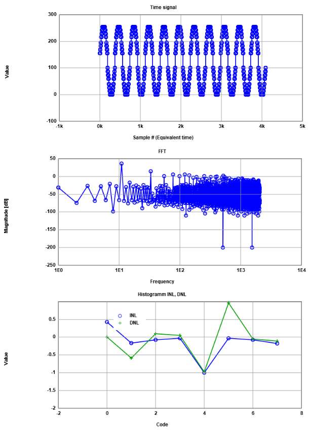
FFT of LTSPICE sine simulation of real ADC DAC Test Circuit
This FFT is done using 3 bit codes only.
Signal to noise is unchanged.
INL, DNL looks more reasonable, but goes up to 1.
Signal level (11): 36.85 dB.
Total noise: 17.44 dB.
First harmonic (33): 14.76 dB.
ENOB = (36.85 - 17.44 -1.76)/6.02 = 2.93 bits.
Video Instructions LTSPICE .Measurement
This video presents the analysis of LTSPICE simulation files with
a .measure statement.
Run the ADC DAC test simulation in LTSPICE with a ramp.
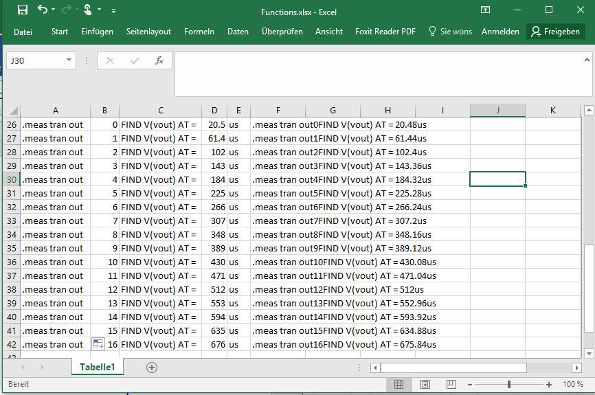
Insert SPICE directive:
.meas trans OUT00 FIND V(vout) AT=81.92us
After simulation "View","SPICE Error log" will show the result.
Multiple measurement statements can be placed into a file.
After simulation "File","Execute .MEAS script" generates the results.
A 10-bit data converter should have about 16384 measurement values.
Data extraction can be difficult and quite time consuming.
Duration 5:55 min
LTSPICE .Measurement
With Excel 16 measurement statements were created.
These were copied to a text editor and saved in a file measure.meas
LTSPICE: File, Execute .MEAS script executes the file.
LTSPICE: View, SPICE Error log shows the results.
Each measurement name needs a unique id.
12:44
.meas tran out0  FIND V(vout) AT = 20.48us
.meas tran out1  FIND V(vout) AT = 61.44us
.meas tran out2  FIND V(vout) AT = 102.4us
.meas tran out3  FIND V(vout) AT = 143.36us
.meas tran out4  FIND V(vout) AT = 184.32us
.meas tran out5  FIND V(vout) AT = 225.28us
.meas tran out6  FIND V(vout) AT = 266.24us
.meas tran out7  FIND V(vout) AT = 307.2us
.meas tran out8  FIND V(vout) AT = 348.16us
.meas tran out9  FIND V(vout) AT = 389.12us
.meas tran out10 FIND V(vout) AT = 430.08us
.meas tran out11 FIND V(vout) AT = 471.04us
.meas tran out12 FIND V(vout) AT = 512us
.meas tran out13 FIND V(vout) AT = 552.96us
.meas tran out14 FIND V(vout) AT = 593.92us
.meas tran out15 FIND V(vout) AT = 634.88us
.meas tran out16 FIND V(vout) AT = 675.84us
View LTSPICE log.
* C:\Users\vollratj\Documents\InEl_Laboratory\web_Template\web_Template\InEl_P2019\2019_GroupY\Measure.mout
out0: V(vout)=0 at 2.048e-005
out1: V(vout)=0.0488599 at 6.144e-005
out2: V(vout)=0.0977199 at 0.0001024
out3: V(vout)=0.14658 at 0.00014336
out4: V(vout)=0.224756 at 0.00018432
out5: V(vout)=0.273616 at 0.00022528
out6: V(vout)=0.322476 at 0.00026624
out7: V(vout)=0.371336 at 0.0003072
out8: V(vout)=0.579805 at 0.00034816
out9: V(vout)=0.628664 at 0.00038912
out10: V(vout)=0.677524 at 0.00043008
out11: V(vout)=0.726384 at 0.00047104
out12: V(vout)=0.80456 at 0.000512
out13: V(vout)=0.85342 at 0.00055296
out14: V(vout)=0.90228 at 0.00059392
out15: V(vout)=0.95114 at 0.00063488

Measurement "out16" FAIL'ed
Summary
Data extraction from LTSPICE is important for calculation of INl, DNL and SNR
The right amount of points with teh desired bit range is needed to get good results.
Ideal sine wave showed good INL and DNL for 15 codes and
expected signal to noise ratio of 25.6 dB.
30% and 50% change in R value showed a DNL=2.3 and INL=1.2
FFT showed 19.4 dB SNR and a low ENOB = 2.93 still not limited by harmonics.
Data extraction can also be done via .meas statements.<\li>
Since this is a DAC INL and DNL between ramp and sine are not exactly matching.<\li>