Laboratory 01/02: Electric, Layout, Schematic and MOS Transistors
Jörg Vollrath
Static IV curves of NMOS and PMOS Transistors from schematic and layout are simulated for \( 1 \mu m \) technology. Electric as design tool is used.
This practical training uses Electric for layout and schematic entry and LTSPICE for simulation. Electric is free software and needs minimal installation and maintenance. There is a standard cell library available muddlib07.jelib , an example for a MIPS processor muddlib07.jelib and operational amplifiers opamp.jelib
. It has many EDA tools built in, has a good tutorial and help system and needs minimum effort to start.
- Electric: http://www.staticfreesoft.com/index.html
- CMOS Circuit Design and Layout: http://www.cmosedu.com/
- LTSPICE: http://www.linear.com/designtools/software/
- David Harris, Harvey Mudd college: MIPS Design, https://globlib4u.wordpress.com/2013/01/26/e158-spring-2007-mips-project/
- David Harris, Harvey Mudd college: MIPS Design, http://www3.hmc.edu/~harris/
- MIPS 2007 http://www.staticfreesoft.com/contrib/muddChip.tar.gz
Electric
This section starts Electric (L:\apps\VLSIDesignSystem\VLSIDesignSystem.bat) and does some basic configuration.
You can either do it manually setting one option at a time or import electricPrefs.xml .
Start Electric by double clicking on the symbol on the desktop. Adjust the windows.
Select a white Background: Window- > Color Schemes - > White background color
Increase Memory: File->Preferences- > General- > General Memory
Maximum Memory 512 megabytes
Maximum permanent space 64 megabytes
Setup Technology:
File->Preferences->Technology->Technology mocmos Metal layers 3 Layers
File->Preferences->Technology->Scale 500 nanometer
Set LTSPICE path:
File->Preferences->Tools->SPICE
Spice engine Spice 3
Spice level: 3
Parasitics: Trans area/perim only
After writing deck: Run, Ignore Output
Run program: L:\apps\LTC\LTspiceIV\scad3.exe
!! Adjust this path to your directory structure !!
with args: -i ${FILENAME} -r ${FILENAME_NO_EXT}.raw -o ${FILENAME_NO_EXT}.out
!! SPACE between the options are needed.
check Use dir: your directory (c:\temp\Microelectronics\Laboratory\SPICE\)
check: Overwrite existing output file (no prompt)
Apply
Export: electricPrefs.xml to your group directory
Simulation of CMOS Transistors
The following simulations should give you the threshold voltages of the NFET and PFET Transistors and the IDS for VGS=VDD.
| Technology | \( 1 \mu m \) | \( 1 \mu m \) | 50nm | 50nm |
| Schematic | Given | Given | Change scale | Change scale |
| LTSPICE transfer curve | Run | Run | Change model | Change model |
| LTSPICE output curve | Change Sim | Change Sim | ||
| Layout | Change scale | Change scale | ||
| LTSPICE transfer curve | ||||
| LTSPICE output curve | ||||
| Transistor | NFET(W/L=20/1) | PFET(W/L=20/1) | NFET(W/L=20/1) | PFET(W/L=20/1) |
| Vth | ||||
| IDS(VGS = VDS = VDD) |
Schematic and Layout of a MOS Transistor
This section shows how to simulate the output curve of a MOS Transistor.
Copy the files: cmosedu_models.txt and Lab01_1u_00.jelib to your personal directory.
Open the Library Lab01_1u_00.jelib.
Select in the Explorer Tab NFET_1u_IV{sch}.
Tools->Simulation(SPICE)->Write SPICE Deck. This starts LTSPICE. Watch the message window for errors.
If there is an error in LTSPICE delete the .OPTION line.
Error message: Can't find transistor model
Open cmosedu_models.txt in LTSPICE (type .txt *.*) and check model.
If the file cmosedu_models.txt does not exist, copy the file to this location.
Make sure the node names of the transistor match the node names of the voltage sources, otherwise you have floating nodes and no current will flow.
You have to hit the run button to start the SPICE simulation. A graphical window appears where you do a 'Add Trace' with the current I(VDS).
Look at the output IV-curve of a MOSFET. X-Axis VDS, y axis IDS. Make a printout for your report.
Note down the IDS. Exchange the position of VDS and VGS voltage variations in the .dc statement and look at the transfer characteristic. Note down the threshold voltage. You can vary the source VWS to see a change in the threshold voltage.
Close LTSPICE.
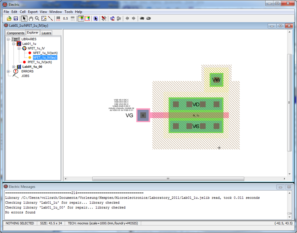
NMOS Transistor Layout
We will design the corresponding layout for the NFET transistor.
Cell->New Cell.. -> select layout, set name NFET_1u_IV same name as schematic.
Goto:
Components select nMOS Transistor and place it.
On the bottom of the screen you see a small text what kind of object you are selecting.
Size the transistor: Double click on the transistor to change width to 20.
Specify the transistor model: Tools -> Simulation (Spice) -> Set Spice Model -> N_1u
Holding down the <Strg> key lets you cycle through all possible selections.
Place the source drain contacts: select nACT and place a contact above the transistor and below the transistor. Resize the contacts to 20 by double clicking on them (Edit->Properties-> Object Properties)
Place a gate contact. Select 'Metal-1-Polysilicon Contact' to the left of the transistor.
Connect the contacts with the transistor: Select the contact. Press and hold the right mouse button and draw a connection to the transistor. If the wire gets to wide, Select the wire, double click and select at the end extension neither end.
Do a design rule check via Tools-> DRC-> Check Hierarchically (F5)
Name the wires: double click on the wires and name the connection G, D, S
Export the pins: Select the contacts, Export->Create Export, Export name VG, VD, VS, VW and set the characteristics to input or bidirectional.
Spice Code: Insert the SPICE code via Misc-> SPICE code or copy it from the schematic.
Simulate the output characteristics: Tools->Simulation(SPICE)-> write SPICE deck.
Make sure the node names of the transistor match the node names of the voltage sources, otherwise you have floating nodes and no current will flow.
Make sure to use the right transistor model: L, W of NFET PFET should match model name of NFET, PFET and model name in cmoseedu_models.txt.
Layout versus Schematic and 3D View
To check the layout versus schematic use Tools->NCC-> Schematic and Layout Views
The checklist can be defined under Preferences->Tools->NCC
If a layout view is active a 3D view can be generated using Window->3D Window-> 3D View.
Output and Transfer curves for PFET
Select in the Explorer Tab PFET_1u_IV{sch}.
Tools->Simulation(SPICE)->Write SPICE Deck. This starts LTSPICE. Watch the message window for errors.
If there is an error in LTSPICE delete the .OPTION line. You have to hit the run button to start the SPICE simulation. A graphical window appears where you do a 'Add Trace' with the current I(Vds).
Look at the output IV-curve of a MOSFET. X-Axis VDS, y axis IDS. Make a printout for your report.
Note down IDS. Exchange the position of VDS and VGS voltage variations in the .dc statement and look at the transfer characteristic. Note the threshold voltage. You can vary the source VWS to see a change in the threshold voltage.
Make sure the node names of the transistor match the node names of the voltage sources, otherwise you have floating nodes and no current will flow.
Make sure to use the right transistor model: L, W of NFET PFET should match model name of NFET, PFET and model name in cmoseedu_models.txt.
Simulations for 50nm Technology
Use the SPICE simulation code for 1µm Technology and change the transistors.
MM1 VD VG 0 VW N_50n L=50n W=1U
MM1 VD VG 0 VW P_50n L=50n W=1U
Simulate output and transfer characteristic between 0..1 V and extract threshold voltage and IDS(VGS=VDS=1V). What happens at voltages between 1 V and 5 V?
Make sure the node names of the transistor match the node names of the voltage sources, otherwise you have floating nodes and no current will flow.
Make sure to use the right transistor model: L, W of NFET PFET should match model name of NFET, PFET and model name in cmoseedu_models.txt.
Report
Example: Documentation format
The report should include
1) Your experience during the practical training.
What obstacles did you experience how did you solve them? Please work in groups. You should also note down times you spent for each task.
2) Screenshots of the output and transfer curves of NFET and PFET in 50nm and 1um. Layout of the NFET and PFET. A nice 3D view of a PFET with some explanations. Extract threshold voltage and maximum currents for the transistors. What happens if you operate a transistor in 50nm technology at 5V?
Please send your electronic report as pdf including your name and lab number to joerg.vollrath@hs-kempten.de.
The filename should be <year>_Lab01_<Name>.pdf until 29.4.2024.
You can use PDFCreator as printer for creating pdf files via the print menue in Windows.
Microelectronics
Laboratory 03/04