
Open Laboratory 2018: Tiny FPGA
Joerg VollrathLaboratory Instructions
Build a very tiny FPGA with minimum size 50 nm transistors.
A minimum schematic is shown above. The FPGA is configured using a scan operation. With TE active serial data is fed into TDI and shifted through all scan cells for FPGA configuration.
- General specification
- n LUT2 blocks
- m IO pads
- Global pins: VDD, GND, CLK, CE, RST
- Test and configuration: TE, TDI, TDO
- Switch matrix
- 1 input 4 outputs DEMUX
- 4 inputs 1 output MUX
- 2 input, 1 output LUT2 with register (out Y) and 1 shift register (out YS)
Start: 2 inputs, 2 outputs, one LUT, 4 input switch matrix, 4y output switch matrix
What is the relationship between number of pins, switch matrix and LUTs?
What would be the optimum number of global lines, inputs/outputs for switch matrix and LUTs?
Implement a state machine or truth table in FPGA.
Overview and tool chain
The sclib.jelib provides basic logic functions and a scan cell flip flop.A schematic for circuit A or B is created and fully tested with simulation.
LTSPICE and IRSIM are used for simulation. Delay times are extracted and compared.
Architecture exploration for relationship between number of pins, switch matrix and LUTs is done using literature research, graphs, excel, empty blocks and/or JavaScript.
Layout will be generated using the silicon compiler.
Routing will be done with the routing tool.
Pads will be placed to generate a chip using pad frame generator tool.
Schematic block generation
In a schematic a cell from another library can be placed with Misc. -> Cell Instance ..The scan cells share the same TE. TDO from one cell is connected to TDI of the next cell.
For FPGA output Q of one cell is connected to D of the same cell.
Please use only scan cells instead of registers/D-flipflops.
Label interesting internal signals, wires for simulation.
Provide a description of the hook up of scan cells.
Create exports for inputs and outputs.
Check the exports with 'Exports','Manipulate exports'.
TLUT2 block
This block has 4 scan cell registers (LR0..LR3) to program a truth table.The input x1 and x2 selects, which information (LR0..LR3) is transfered to the output register YR with a rising clock edge.
x1,x2 are the control signals for a multiplexer with LR0..LR3 as inputs and YR as output.
An additional shift register YS stores the information Y from previous clock cycle.
TMUX block
This block has 2 registers (MR0,MR1) to program a connection between x1..x4 and Y.MR0,MR1 are the control signals for a multiplexer with x1..x4 as inputs and y as output.
TDEMUX block
This block has 2 registers (DR0,DR1) to program a connection between x and y1..y4.DR0,DR1 are the control signals for a demultiplexer with x as input and y1..y4 as outputs.
You can use logic cells or switches (switch2a).
Simulate behavior using LTSPICE
Make a test plan.Program the registers using TE and CLK.
Apply all input patterns and observe the output.
Connect inverters to inputs and outputs to achieve a realistic input voltage source and output load and measure delay times from CLK or input to output.
Simulate behavior using IRSIM
IRSIM is started with tools built in simulator.Selecting a pin and moving the cursor to a time keys V, G can set the output level to high or low. Also the menue tools-> built in simulation, set IRSIM to high/low can be used.
Output can also be probed.
A typical IRSIM file looks like:
l I0
l I1
s 2.0
h I0
s 2.0
h I1
s 2.0
l I0
h I1: sets pin I1 to '1' high.
s 2.0: performs a time step of 2.0 ns.
The example sets I0 and I1 to '0', waits 2 ns and then set I0 to '1'.
After another 2ns I1 is set to '1'.
You can create LTSPICE and IRSIM stimuli with test vector generation. Verify matching of LTSPICE and IRSIM simulation.
Do a High-Z output test with resistance to GND, VDD or VDD/2.
Long LTSPICE text shrinks the schematic and layout drawing. Use
FPGA Schematic
Create a minimum schematic fpga_tiny with: 2 IO pins, one LUT2, 2 input switch matrices, 2 output switch matrices as shown in the top picture.Synthesize core circuit and simulate without pads
Select M1 in another cell to enable the right layers for routing.Select fpga_tiny{vhdl}.
Tools-> Silicon Compiler -> Convert current cell to layout.
In the VHDL code delete all entities and architectures of cells which have already a layout.
If you have used PFET or NFET transistors create layouts for these cells.
For simulation create a new cell fpga_tiny doc.waveform.
In the tab 'Components' place the cell fpga_tiny layout.
LTSPICE simulation
Add the LTSPICE simulation text:
.include cmosedu_models.txt
.global VDD
VDD VDD 0 DC 1
VCLK CLK 0 PULSE(0 1 0 1n 1n 19n 40n)
VCLR RESET 0 PULSE(0 1 0 1n 1n 99n 2000n)
.tran 1000n
Add further stimuli for testing functionality.
Do a LTSPICE simulation to check functionality.
Since the top level cell needs some inputs modify the line
*** TOP LEVEL CELL: mod_m_counter{doc.wave}
Xfpga_tiny@0 clk gnd max_tick q__0 q__1 q__2 q__3 reset vdd fpga_tiny
accordingly.
Document your simulation result.
Repeat simulation with RCX extraction.
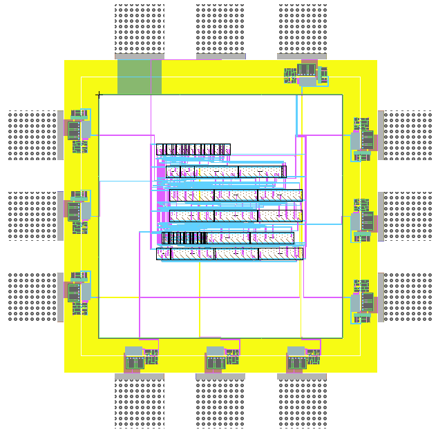
Create a chip adding Pads (, test structures and alignment marks)
Use the library Pads4u.jelib.
Tools->Padframe
Create a pad frame placing file (.arr) according to Help.
Deliverables
Document your laboratory in a pdf document with a name of < Date > _2019_FPGA_ < name > .pdf
and send it to joerg.vollrath@hs-kempten.de.
A maximum of 2 students can prepare a document together clearly marking authorship
of different sections. Submission is due 10.7.2019.
- Schematic of switch matrix or LUT
- LTSPICE (and IRSIM) simulation of this block with extensive comments
- < Name > .jelib with Chip_FPGA, FPGA, LUT2 or MUX41 and DEMUX14 and simulation code
- LTSPICE simulation of FPGA.
- Discussion of architecture options.
- Table listing time efforts to complete the laboratory.
- Summary
Result
Layout Renderer
Summary and Discussion
Accomplishments:
- A tool can convert a truth/state table in a LTSPICE/IRSIM simulation file.
- Benefits of an automated toolchain were experienced.
- A circuit was placed in an IO-Pad frame
- Test and scan cell operation was simulated.
- A basic layout renderer for HTML5 was created.
- Discovery of IRSIM technology files:
300nm
First try modification for 50nm
Open Challenges:
- Provide a working IO-Pad simulation
- Make real IO-Pads
- Provide working IRSIM simulations with expected output
- Provide Chip id and test structures.
First try modification for 50nm