
Open Laboratory 2018: Tiny FPGA
Joerg VollrathLaboratory Instructions
Build a very tiny FPGA with minimum size 50 nm transistors.
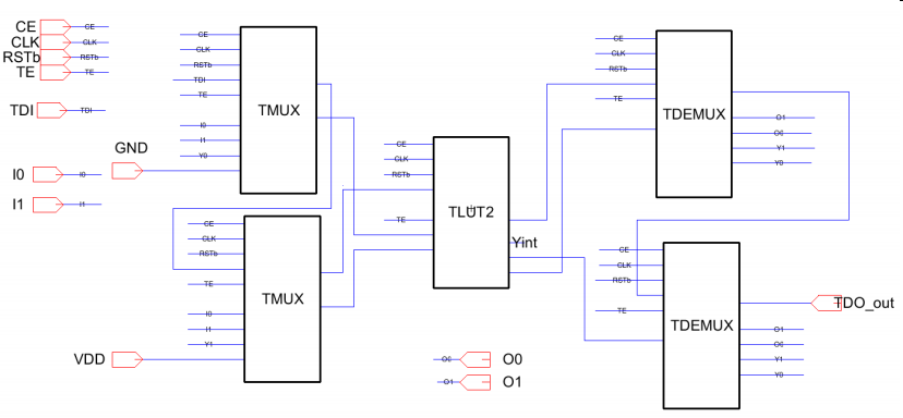
A minimum schematic is shown above. The FPGA is configured using a scan operation. With TE active serial data is fed into TDI and shifted through all scan cells for FPGA configuration.
- General specification
- n LUT2 blocks
- m IO pads
- Global pins: VDD, GND, CLK, CE, RST
- Test and configuration: TE, TDI, TDO
- Switch matrix
- 1 input 4 outputs DEMUX
- 4 inputs 1 output MUX
- 2 input, 1 output LUT2 with register (out Y) and 1 shift register (out YS)
Overview and tool chain
The sclib.jelib provides basic logic functions and a scan cell flip flop.A schematic for circuit A or B is created and fully tested with simulation.
LTSPICE and IRSIM are used for simulation. Delay times are extracted and compared.
Architecture exploration for relationship between number of pins, switch matrix and LUTs is done using literature research, graphs, excel, empty blocks and/or JavaScript.
Layout will be generated using the silicon compiler.
Routing will be done with the routing tool.
Pads will be placed to generate a chip using pad frame generator tool.
Schematic block generation
In a schematic a cell from another library can be placed with Misc. -> Cell Instance ..The scan cells share the same TE. TDO from one cell is connected to TDI of the next cell.
For FPGA output Q of one cell is connected to D of the same cell.
Please use only scan cells instead of registers/D-flipflops.
Label interesting internal signals, wires for simulation.
Provide a description of the hook up of scan cells.
Create exports for inputs and outputs.
Check the exports with 'Exports','Manipulate exports'.
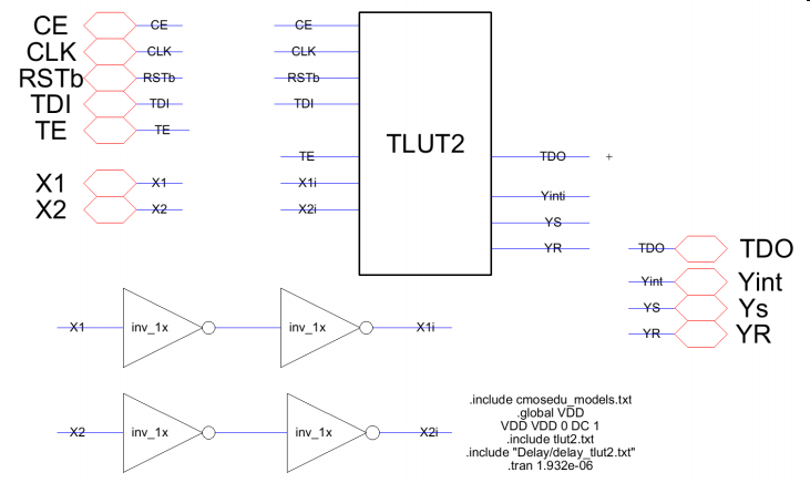
TLUT2 block
This block has 4 scan cell registers (LR0..LR3) to program a truth table.The input x1 and x2 selects, which information (LR0..LR3) is transfered to the output register YR with a rising clock edge.
x1,x2 are the control signals for a multiplexer with LR0..LR3 as inputs and YR as output.
An additional shift register YS stores the information Y from previous clock cycle.
TMUX block
This block has 2 registers (MR0,MR1) to program a connection between x1..x4 and Y.MR0,MR1 are the control signals for a multiplexer with x1..x4 as inputs and y as output.
TDEMUX block
This block has 2 registers (DR0,DR1) to program a connection between x and y1..y4.DR0,DR1 are the control signals for a demultiplexer with x as input and y1..y4 as outputs.
You can use logic cells or switches (switch2a).
Simulate behavior using LTSPICE
Make a test plan.Program the registers using TE and CLK.
Apply all input patterns and observe the output.
Connect inverters to inputs and outputs to achieve a realistic input voltage source and output load and measure delay times from CLK or input to output.
Simulate behavior using IRSIM
IRSIM is started with tools built in simulator.Selecting a pin and moving the cursor to a time keys V, G can set the output level to high or low. Also the menue tools-> built in simulation, set IRSIM to high/low can be used.
Output can also be probed.
A typical IRSIM file looks like:
l I0
l I1
s 2.0
h I0
s 2.0
h I1
s 2.0
l I0
h I1: sets pin I1 to '1' high.
s 2.0: performs a time step of 2.0 ns.
The example sets I0 and I1 to '0', waits 2 ns and then set I0 to '1'.
After another 2ns I1 is set to '1'.
You can create LTSPICE and IRSIM stimuli with test vector generation. Verify matching of LTSPICE and IRSIM simulation.
Do a High-Z output test with resistance to GND, VDD or VDD/2.
Long LTSPICE text shrinks the schematic and layout drawing. Use
FPGA Schematic
Create a minimum schematic fpga_tiny with: 2 IO pins, one LUT2, 2 input switch matrices, 2 output switch matrices as shown in the top picture.Synthesize core circuit and simulate without pads
Select M1 in another cell to enable the right layers for routing.Select fpga_tiny{vhdl}.
Tools-> Silicon Compiler -> Convert current cell to layout.
In the VHDL code delete all entities and architectures of cells which have already a layout.
If you have used PFET or NFET transistors create layouts for these cells.
For simulation create a new cell fpga_tiny doc.waveform.
In the tab 'Components' place the cell fpga_tiny layout.
LTSPICE simulation
Add the LTSPICE simulation text:
.include cmosedu_models.txt
.global VDD
VDD VDD 0 DC 1
VCLK CLK 0 PULSE(0 1 0 1n 1n 19n 40n)
VCLR RESET 0 PULSE(0 1 0 1n 1n 99n 2000n)
.tran 1000n
Add further stimuli for testing functionality.
Do a LTSPICE simulation to check functionality.
Since the top level cell needs some inputs modify the line
*** TOP LEVEL CELL: mod_m_counter{doc.wave}
Xfpga_tiny@0 clk gnd max_tick q__0 q__1 q__2 q__3 reset vdd fpga_tiny
accordingly.
Document your simulation result.
Repeat simulation with RCX extraction.
Create a chip adding Pads (, test structures and alignment marks)
Use the library Pads4u.jelib.
Tools->Padframe
Create a pad frame placing file (.arr) according to Help.
Deliverables
Document your laboratory in a pdf document with a name of < Date > _2019_FPGA_ < name > .pdf
and send it to joerg.vollrath@hs-kempten.de.
A maximum of 2 students can prepare a document together clearly marking authorship
of different sections. Submission is due 10.7.2019.
- Schematic of switch matrix or LUT
- LTSPICE (and IRSIM) simulation of this block with extensive comments
- < Name > .jelib with Chip_FPGA, FPGA, LUT2 or MUX41 and DEMUX14 and simulation code
- LTSPICE simulation of FPGA.
- Discussion of architecture options.
- Table listing time efforts to complete the laboratory.
- Summary
Result
Layout Renderer
Review Strategy
- Create table for topics and students
- Gather topics and options from reports
- Review reports with full list and generate best web page
- Final grading
The documentation should have schematics, state tables and simulations for MUX, DEMUX and LUT.
The flow of documentation can be circuit based (this example) or
task (schematic, state table, simulation) based.
Introduction
The results presented here are developed in order according to the procedure described in the guide:
https://personalpages.hs-kempten.de/~vollratj/Microelectronics/2018_Lab_Micro_FPGA.html. If
additional steps were required, description of these will be given.
- Open Electric
- Load the library scelib
- Set the preferences according to the laboratory instructions
- Create a new library tinyfpga
- Create new cells for the MUX, DEMUX and LUT2
- Design the schematic of the cells, by using IC´s of the scelib library
- Connect the IC´s in the right way
- Name the internal signals
- Create exports for all the inputs and outputs of the schematic
For the creation of blocks, a new library called "tinyfpga.jelib" was created in
Electric software.
There, the blocks were created and simulated.
The library "sclib.jelib" is also needed for the working of the
program, as the basic blocks used in tinyfpga are provided by this library.
For all the blocks generated, the signal TE, TDI, and TDO work in the same way.
The following table resumes their functionality in the program.
| Signal | Brief functionality description | |
| TE | Input | Test Enable. Enables the test functionality in the scan cells, allowing to pass the data in TDI to the output Q and TDO. |
| TDI | Input | Test Data input. Data to be transferred into the output Q and TDO with a rising clock edge. |
| TDO | Output | Test Data output. Data transferred from the TDI. |
Mainly, for schematic generation, the following instructions were applied to the schematic according to the lab instructions.
- Scan cells share the same TE signal.
- TDO from one cell is connected to TDI of the next cell, in order to configure the data from all the cells with a serial communication.
- For the output Q of the register, is connected to the input D of the same cell. In this way, the information remains stored in the register after data initialization.
MUX schematic
|
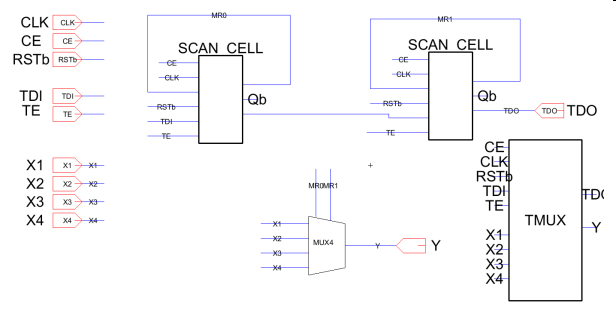 |
| TMUX Block state table | |||
| MR1 | MR2 | Y | |
| 0 | 0 | X1 | |
| 0 | 1 | X2 | |
| 1 | 0 | X3 | |
| 1 | 1 | X4 | |
TDEMUX schematic
|
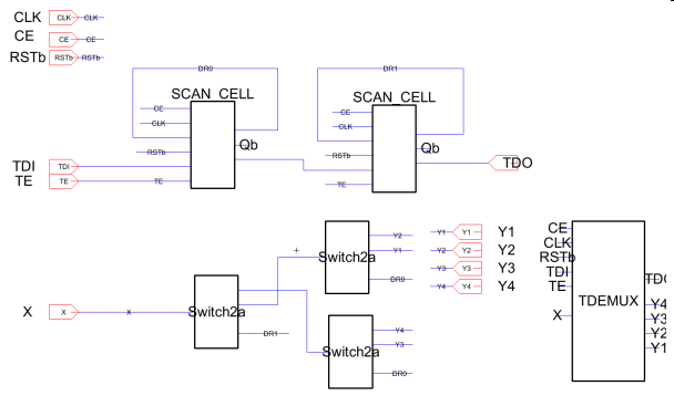 |
| DEMUX Block truth table | ||||||
| MR1 | MR0 | Y1 | Y2 | Y3 | Y4 | |
| 0 | 0 | X | High-Z | High-Z | High-Z | |
| 0 | 0 | High-Z | X | High-Z | High-Z | |
| 0 | 0 | High-Z | High-Z | X | High-Z | |
| 0 | 0 | High-Z | High-Z | High-Z | X | |
LUT schematic
|
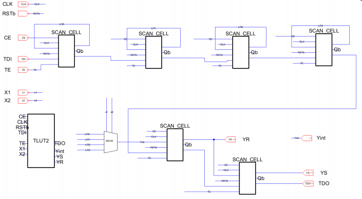 |
| TLUT2 Block state table | ||||||||
| LR0 | LR1 | LR2 | LR3 | X1 | X2 | Yn+1 | YSn+1 | |
| X | X | X | X | 0 | 0 | LR3 | Yn | |
| X | X | X | X | 0 | 1 | LR2 | Yn | |
| X | X | X | X | 1 | 0 | LR1 | Yn | |
| X | X | X | X | 1 | 1 | LR0 | Yn | |
As seen in the schematic the scan cells have the sequence: LR0, LR1, LR2, LR3, Y, YS

Tinyfpga library overview
The following image shows the created library and its contents: TF_DEMUX, TF_LUT2 and TF_MUX blocks contains the schematic {sch} and icon view {ic}. Additional schematics TF_DEMUX_test, TF_LUT2_test and TF_MUX_test contain the simulation of the logic of the blocks.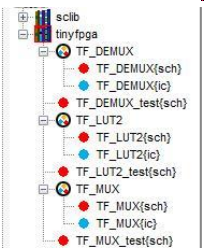
Simulation
For the simulation of the blocks, additional steps were required. These steps can be summarized as power and analysis request, export creation, vector generation, circuit conditioning, and results.Basic procedure
To do the functional testing of the components according to the laboratory instructions, for every component the same procedure was applied:- Open Electric and load the tinyfpga and sclib libraries
- Create an additional test-cell in the tinyfpga library for each component
- Place the IC of the component to be tested in this schematic
- Create the exports for the inputs and outputs of the IC
- Add two LTSpice codes (one for the LTSpice simulation text and one to include the stimuli for functional testing) to the schematic, by selecting Components ? Misc. ? Spice Code
- Create individual test-vectors for each component (e.g. with Excel)
- Use the online tool test vector generation to create LTSpice code out of the test- vectors created with Excel
- Insert the created Spice code in one of the Spice Code fields
- Modify the simulation text according to the signal duration, mentioned in the vector generation
- Start the simulation and debug the component in an iterative process, until the desired functionality is achieved
Power and analysis request
An additional schematic for simulation is required. Additional to the block to test, a code for power and analysis definition is needed.
.global vdd
VDD VDD 0 DC 1
.include cmosedu_models.txt
.tran 0 800n 0 0.01n
Figure - Code for Power and Analysis In this code, the power definition is set up, the model of the transistor is included, and a transient analysis is requested. The time needed for the analysis depends on the logic and test vectors, therefore this parameter varies for each block tested.
Power and analysis request
In order to control and change the values for the inputs and observe the outputs in the analysis, the creation of the exports is required.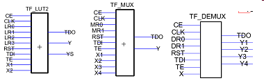
As it is expected, the export match with the input and output names.
Test vector generation
Now that the exports were created, an additional code was needed for control the input signals and compare the output to the expected values. In order to do that, the philosophy to test can be described in the following flow chart:
With the previous idea, the following vectors were created. The states will be indicated in different colors, indicating the key data input.
- Reset:
In this state, all the memory cells are set to zero and "erased" from previous states. The input reset (RST) is enabled to do this action. No output is expected. After 1 clock period, the signal is disabled. - Memory cell configuration:
Memory can be set up to a desired state. Depending on the block of test, this step can setup the memory control signals (TF_MUX, TF_DEMUX), or the memory input signals (TF_LUT2). During this state the clock enable (CE) and test enable (TE) are activated. To configure the desired data, the input TDI is used as a serial communication, and in order to reach the proper memory, the sequence TDI to TDO must be taken into account. The number of clock periods needed for this state, depends on the configuration of the block, as well as, the desired setup. - Input combination and output visualization:
Input to the blocks can now be set to different combinations, and the output can be compared. In this state, the signal TE is always desactivated. If the output depends on registers, the signal CE must be activated in order to allow the logic to feed an output register. If it not depend on register, the signal CE must be disactivated, as the output does not depend on clock cycle. If more simulation cases are needed, the process can start again to the reset state.
It must be said also, that this is not a complete test, as a complete test requires all the possible combinations of inputs. Therefore, is only limited to these specific combinations.
Circuit conditioning
Additional to the steps before, the block TF_LUT2 required a special condition at the outputs. This is because all the outputs are not constantly updated at the same time. Instead, through the configuration of the switches, only one of the outputs get an updated value. Therefore, the other outputs should be in an indeterminate state of 0.5V, not 0 and not 1. In order to get this idea, a resistive circuit was adapted.If the resistance is to high, tristate will show slow convergence to 0.5V.
If the resistance is to low, 0V and Vdd can not be reached.
50k was used.

Generating vectors and TestJS
For all circuits state tables for minimum testing were created.
Each row in the table will be one clock cycle in simulation and displayed as one column.
| Test vector generation for TMUX block | Input for TestJS | |||||||||
| RST | CE | TE | TDI | X1 | X2 | X3 | X4 | xY | RST,CE,TE,TDI,X1,X2,X3,X4;xY,Comment | |
| 0 | 0 | 0 | 0 | 0 | 0 | 0 | 0 | 0 | 0,0,0,0,0,0,0,0;0,Reset | |
| 1 | 1 | 1 | 0 | 0 | 0 | 0 | 0 | 0 | 1,1,1,0,0,0,0,0;0,Registers 00 | |
| 1 | 1 | 1 | 0 | 0 | 0 | 0 | 0 | 0 | 1,1,1,0,0,0,0,0;0,Registers 01 | |
| 1 | 0 | 0 | 0 | 0 | 0 | 0 | 0 | 0 | 1,0,0,0,0,0,0,0;0,xY=X1 | |
| 1 | 0 | 0 | 0 | 0 | 0 | 0 | 1 | 0 | 1,0,0,0,0,0,0,1;0,xY=X1 | |
| 1 | 0 | 0 | 0 | 0 | 0 | 1 | 0 | 0 | 1,0,0,0,0,0,1,0;0,xY=X1 | |
| 1 | 0 | 0 | 0 | 0 | 0 | 1 | 1 | 0 | 1,0,0,0,0,0,1,1;0,xY=X1 | |
| 1 | 0 | 0 | 0 | 0 | 1 | 0 | 0 | 0 | 1,0,0,0,0,1,0,0;0,xY=X1 | |
| 1 | 0 | 0 | 0 | 0 | 1 | 0 | 1 | 0 | 1,0,0,0,0,1,0,1;0,xY=X1 | |
| 1 | 0 | 0 | 0 | 0 | 1 | 1 | 0 | 0 | 1,0,0,0,0,1,1,0;0,xY=X1 | |
| 1 | 0 | 0 | 0 | 0 | 1 | 1 | 1 | 0 | 1,0,0,0,0,1,1,1;0,xY=X1 | |
| 1 | 0 | 0 | 0 | 1 | 0 | 0 | 0 | 1 | 1,0,0,0,1,0,0,0;1,xY=X1 | |
| 1 | 0 | 0 | 0 | 1 | 0 | 0 | 1 | 1 | 1,0,0,0,1,0,0,1;1,xY=X1 | |
| 1 | 0 | 0 | 0 | 1 | 0 | 1 | 0 | 1 | 1,0,0,0,1,0,1,0;1,xY=X1 | |
| 1 | 0 | 0 | 0 | 1 | 0 | 1 | 1 | 1 | 1,0,0,0,1,0,1,1;1,xY=X1 | |
| 1 | 0 | 0 | 0 | 1 | 1 | 0 | 0 | 1 | 1,0,0,0,1,1,0,0;1,xY=X1 | |
| 1 | 0 | 0 | 0 | 1 | 1 | 0 | 1 | 1 | 1,0,0,0,1,1,0,1;1,xY=X1 | |
| 1 | 0 | 0 | 0 | 1 | 1 | 1 | 0 | 1 | 1,0,0,0,1,1,1,0;1,xY=X1 | |
| 1 | 0 | 0 | 0 | 1 | 1 | 1 | 1 | 1 | 1,0,0,0,1,1,1,1;1,xY=X1 | |
| 0 | 0 | 0 | 0 | 0 | 0 | 0 | 0 | 0 | 0,0,0,0,0,0,0,0;0,Reset | |
| 1 | 1 | 1 | 0 | 0 | 0 | 0 | 0 | 0 | 1,1,1,0,0,0,0,0;0,Set registers to 01 | |
| 1 | 1 | 1 | 1 | 0 | 0 | 0 | 0 | 0 | 1,1,1,1,0,0,0,0;0,Set registers to 01 | |
| 1 | 0 | 0 | 0 | 0 | 0 | 0 | 0 | 0 | 1,0,0,0,0,0,0,0;0,xY=X2 | |
| 1 | 0 | 0 | 0 | 0 | 0 | 0 | 1 | 0 | 1,0,0,0,0,0,0,1;0,xY=X2 | |
| 1 | 0 | 0 | 0 | 0 | 0 | 1 | 0 | 0 | 1,0,0,0,0,0,1,0;0,xY=X2 | |
| 1 | 0 | 0 | 0 | 0 | 0 | 1 | 1 | 0 | 1,0,0,0,0,0,1,1;0,xY=X2 | |
| 1 | 0 | 0 | 0 | 0 | 1 | 0 | 0 | 1 | 1,0,0,0,0,1,0,0;1,xY=X2 | |
| 1 | 0 | 0 | 0 | 0 | 1 | 0 | 1 | 1 | 1,0,0,0,0,1,0,1;1,xY=X2 | |
| 1 | 0 | 0 | 0 | 0 | 1 | 1 | 0 | 1 | 1,0,0,0,0,1,1,0;1,xY=X2 | |
| 1 | 0 | 0 | 0 | 0 | 1 | 1 | 1 | 1 | 1,0,0,0,0,1,1,1;1,xY=X2 | |
| 1 | 0 | 0 | 0 | 1 | 0 | 0 | 0 | 0 | 1,0,0,0,1,0,0,0;0,xY=X2 | |
| 1 | 0 | 0 | 0 | 1 | 0 | 0 | 1 | 0 | 1,0,0,0,1,0,0,1;0,xY=X2 | |
| 1 | 0 | 0 | 0 | 1 | 0 | 1 | 0 | 0 | 1,0,0,0,1,0,1,0;0,xY=X2 | |
| 1 | 0 | 0 | 0 | 1 | 0 | 1 | 1 | 0 | 1,0,0,0,1,0,1,1;0,xY=X2 | |
| 1 | 0 | 0 | 0 | 1 | 1 | 0 | 0 | 1 | 1,0,0,0,1,1,0,0;1,xY=X2 | |
| 1 | 0 | 0 | 0 | 1 | 1 | 0 | 1 | 1 | 1,0,0,0,1,1,0,1;1,xY=X2 | |
| 1 | 0 | 0 | 0 | 1 | 1 | 1 | 0 | 1 | 1,0,0,0,1,1,1,0;1,xY=X2 | |
| 1 | 0 | 0 | 0 | 1 | 1 | 1 | 1 | 1 | 1,0,0,0,1,1,1,1;1,xY=X2 | |
| 0 | 0 | 0 | 0 | 0 | 0 | 0 | 0 | 0 | 0,0,0,0,0,0,0,0;0,Reset | |
| 1 | 1 | 1 | 1 | 0 | 0 | 0 | 0 | 0 | 1,1,1,1,0,0,0,0;0,Set registers to 10 | |
| 1 | 1 | 1 | 0 | 0 | 0 | 0 | 0 | 0 | 1,1,1,1,0,0,0,0;0,Set registers to 10 | |
| 1 | 0 | 0 | 0 | 0 | 0 | 0 | 0 | 0 | 1,0,0,0,0,0,0,0;0,xY=X3 | |
| 1 | 0 | 0 | 0 | 0 | 0 | 0 | 1 | 0 | 1,0,0,0,0,0,0,1;0,xY=X3 | |
| 1 | 0 | 0 | 0 | 0 | 0 | 1 | 0 | 1 | 1,0,0,0,0,0,1,0;1,xY=X3 | |
| 1 | 0 | 0 | 0 | 0 | 0 | 1 | 1 | 1 | 1,0,0,0,0,0,1,1;1,xY=X3 | |
| 1 | 0 | 0 | 0 | 0 | 1 | 0 | 0 | 0 | 1,0,0,0,0,1,0,0;0,xY=X3 | |
| 1 | 0 | 0 | 0 | 0 | 1 | 0 | 1 | 0 | 1,0,0,0,0,1,0,1;0,xY=X3 | |
| 1 | 0 | 0 | 0 | 0 | 1 | 1 | 0 | 1 | 1,0,0,0,0,1,1,0;1,xY=X3 | |
| 1 | 0 | 0 | 0 | 0 | 1 | 1 | 1 | 1 | 1,0,0,0,0,1,1,1;1,xY=X3 | |
| 1 | 0 | 0 | 0 | 1 | 0 | 0 | 0 | 0 | 1,0,0,0,1,0,0,0;0,xY=X3 | |
| 1 | 0 | 0 | 0 | 1 | 0 | 0 | 1 | 0 | 1,0,0,0,1,0,0,1;0,xY=X3 | |
| 1 | 0 | 0 | 0 | 1 | 0 | 1 | 0 | 1 | 1,0,0,0,1,0,1,0;1,xY=X3 | |
| 1 | 0 | 0 | 0 | 1 | 0 | 1 | 1 | 1 | 1,0,0,0,1,0,1,1;1,xY=X3 | |
| 1 | 0 | 0 | 0 | 1 | 1 | 0 | 0 | 0 | 1,0,0,0,1,1,0,0;0,xY=X3 | |
| 1 | 0 | 0 | 0 | 1 | 1 | 0 | 1 | 0 | 1,0,0,0,1,1,0,1;0,xY=X3 | |
| 1 | 0 | 0 | 0 | 1 | 1 | 1 | 0 | 1 | 1,0,0,0,1,1,1,0;1,xY=X3 | |
| 1 | 0 | 0 | 0 | 1 | 1 | 1 | 1 | 1 | 1,0,0,0,1,1,1,1;1,xY=X3 | |
| 0 | 0 | 0 | 0 | 0 | 0 | 0 | 0 | 0 | 0,0,0,0,0,0,0,0;0,Reset | |
| 1 | 1 | 1 | 1 | 0 | 0 | 0 | 0 | 0 | 1,1,1,1,0,0,0,0;0,Set registers to 10 | |
| 1 | 1 | 1 | 1 | 0 | 0 | 0 | 0 | 0 | 1,1,1,1,0,0,0,0;0,Set registers to 10 | |
| 1 | 0 | 0 | 0 | 0 | 0 | 0 | 0 | 0 | 1,0,0,0,0,0,0,0;0,xY=X4 | |
| 1 | 0 | 0 | 0 | 0 | 0 | 0 | 1 | 1 | 1,0,0,0,0,0,0,1;1,xY=X4 | |
| 1 | 0 | 0 | 0 | 0 | 0 | 1 | 0 | 0 | 1,0,0,0,0,0,1,0;0,xY=X4 | |
| 1 | 0 | 0 | 0 | 0 | 0 | 1 | 1 | 1 | 1,0,0,0,0,0,1,1;1,xY=X4 | |
| 1 | 0 | 0 | 0 | 0 | 1 | 0 | 0 | 0 | 1,0,0,0,0,1,0,0;0,xY=X4 | |
| 1 | 0 | 0 | 0 | 0 | 1 | 0 | 1 | 1 | 1,0,0,0,0,1,0,1;1,xY=X4 | |
| 1 | 0 | 0 | 0 | 0 | 1 | 1 | 0 | 0 | 1,0,0,0,0,1,1,0;0,xY=X4 | |
| 1 | 0 | 0 | 0 | 0 | 1 | 1 | 1 | 1 | 1,0,0,0,0,1,1,1;1,xY=X4 | |
| 1 | 0 | 0 | 0 | 1 | 0 | 0 | 0 | 0 | 1,0,0,0,1,0,0,0;0,xY=X4 | |
| 1 | 0 | 0 | 0 | 1 | 0 | 0 | 1 | 1 | 1,0,0,0,1,0,0,1;1,xY=X4 | |
| 1 | 0 | 0 | 0 | 1 | 0 | 1 | 0 | 0 | 1,0,0,0,1,0,1,0;0,xY=X4 | |
| 1 | 0 | 0 | 0 | 1 | 0 | 1 | 1 | 1 | 1,0,0,0,1,0,1,1;1,xY=X4 | |
| 1 | 0 | 0 | 0 | 1 | 1 | 0 | 0 | 0 | 1,0,0,0,1,1,0,0;0,xY=X4 | |
| 1 | 0 | 0 | 0 | 1 | 1 | 0 | 1 | 1 | 1,0,0,0,1,1,0,1;1,xY=X4 | |
| 1 | 0 | 0 | 0 | 1 | 1 | 1 | 0 | 0 | 1,0,0,0,1,1,1,0;0,xY=X4 | |
| 1 | 0 | 0 | 0 | 1 | 1 | 1 | 1 | 1 | 1,0,0,0,1,1,1,1;1,xY=X4 | |
| Test vector generation for TDEMUX block | ||||||||||
| RSTb | CE | TE | TDI | X | xY1 | xY2 | xY3 | xY4 | RSTb,CE,TE,TDI,X;xY1,xY2,xY3,xY4,Comment | |
| 1 | 1 | 1 | 0 | 0 | 0 | 0 | 0 | 0 | 1,1,1,0,0;0,0,0,0,set register 00 | |
| 1 | 1 | 1 | 0 | 0 | 0 | 0 | 0 | 0 | 1,1,1,0,0;0,0,0,0,set register 00 | |
| 1 | 0 | 0 | 0 | 0 | 0 | 0 | 0 | 0 | 1,1,0,0,0;0,0,0,0,Y1=x | |
| 1 | 0 | 0 | 0 | 1 | 1 | 0 | 0 | 0 | 1,1,0,0,1;1,0,0,0,Y1=x | |
| 1 | 1 | 1 | 1 | 0 | 0 | 0 | 0 | 0 | 1,1,1,0,0;0,0,0,0,set register 01 | |
| 1 | 1 | 1 | 0 | 0 | 0 | 0 | 0 | 0 | 1,1,1,1,0;0,0,0,0,set register 01 | |
| 1 | 0 | 0 | 0 | 0 | 0 | 0 | 0 | 0 | 1,1,0,0,0;0,0,0,0,Y2=x | |
| 1 | 0 | 0 | 0 | 1 | 0 | 1 | 0 | 0 | 1,1,0,0,1;0,1,0,0,Y2=x | |
| 1 | 1 | 1 | 0 | 0 | 0 | 0 | 0 | 0 | 1,1,1,1,0;0,0,0,0,set register 10 | |
| 1 | 1 | 1 | 1 | 0 | 0 | 0 | 0 | 0 | 1,1,1,0,0;0,0,0,0,set register 10 | |
| 1 | 0 | 0 | 0 | 0 | 0 | 0 | 0 | 0 | 1,1,0,0,0;0,0,0,0,Y3=x | |
| 1 | 0 | 0 | 0 | 1 | 0 | 0 | 1 | 0 | 1,1,0,0,1;0,0,1,0,Y3=x | |
| 1 | 1 | 1 | 1 | 0 | 0 | 0 | 0 | 0 | 1,1,1,1,0;0,0,0,0,set register 11 | |
| 1 | 1 | 1 | 1 | 0 | 0 | 0 | 0 | 0 | 1,1,1,1,0;0,0,0,0,set register 11 | |
| 1 | 0 | 0 | 0 | 0 | 0 | 0 | 0 | 0 | 1,1,0,0,0;0,0,0,0,Y4=x | |
| 1 | 0 | 0 | 0 | 1 | 0 | 0 | 0 | 1 | 1,1,0,0,1;0,0,0,1,Y4=x | |
| Test vector generation for TLUT2 block | ||||||||||
| RSTb | CE | TE | TDI | X1 | X2 | xY | xYS | RSTb,CE,TE,TDI,X1,X2;xY,xYS,Comment | ||
| 0 | 0 | 0 | 0 | 0 | 0 | 0 | 0 | 0,0,0,0,0,0;0,0,Reset | ||
| 1 | 1 | 1 | 1 | 0 | 0 | 0 | 0 | 1,1,1,1,0,0;0,0,Register 1000 | ||
| 1 | 1 | 1 | 0 | 0 | 0 | 0 | 0 | 1,1,1,0,0,0;0,0,Register 1000 | ||
| 1 | 1 | 1 | 0 | 0 | 0 | 0 | 0 | 1,1,1,0,0,0;0,0,Register 1000 | ||
| 1 | 1 | 1 | 0 | 0 | 0 | 0 | 0 | 1,1,1,0,0,0;0,0,Register 1000 | ||
| 1 | 1 | 0 | 0 | 1 | 1 | 1 | 0 | 1,1,0,0,1,1;1,0, | ||
| 1 | 1 | 0 | 0 | 1 | 1 | 1 | 1 | 1,1,0,0,1,1;1,1, | ||
| 0 | 0 | 0 | 0 | 0 | 0 | 0 | 0 | 0,0,0,0,0,0;0,0,Reset | ||
| 1 | 1 | 1 | 1 | 0 | 0 | 0 | 0 | 1,1,1,1,0,0;0,0,Register 100 | ||
| 1 | 1 | 1 | 0 | 0 | 0 | 0 | 0 | 1,1,1,0,0,0;0,0,Register 100 | ||
| 1 | 1 | 1 | 0 | 0 | 0 | 0 | 0 | 1,1,1,0,0,0;0,0,Register 100 | ||
| 0 | 1 | 0 | 0 | 0 | 1 | 1 | 0 | 0,1,0,0,0,1;1,0, | ||
| 0 | 1 | 0 | 0 | 0 | 1 | 1 | 1 | 0,1,0,0,0,1;1,1, | ||
| 0 | 0 | 0 | 0 | 0 | 0 | 0 | 0 | 0,0,0,0,0,0;0,0,Reset | ||
| 1 | 1 | 1 | 1 | 0 | 0 | 0 | 0 | 1,1,1,1,0,0;0,0,Register 10 | ||
| 1 | 1 | 1 | 0 | 0 | 0 | 0 | 0 | 1,1,1,0,0,0;0,0,Register 10 | ||
| 0 | 1 | 0 | 0 | 1 | 0 | 1 | 0 | 0,1,0,0,1,0;1,0, | ||
| 0 | 1 | 0 | 0 | 1 | 0 | 1 | 1 | 0,1,0,0,1,0;1,1, | ||
| 0 | 0 | 0 | 0 | 0 | 0 | 0 | 0 | 0,0,0,0,0,0;0,0,Reset | ||
| 1 | 1 | 1 | 1 | 0 | 0 | 0 | 0 | 1,1,1,1,0,0;0,0,Register 1 | ||
| 0 | 1 | 0 | 0 | 0 | 0 | 1 | 0 | 0,1,0,0,0,0;1,0, | ||
| 0 | 1 | 0 | 0 | 0 | 0 | 1 | 1 | 0,1,0,0,0,0;1,1, | ||
According to these state tables, through the vector creation available in the laboratory instructions (https://personalpages.hs-kempten.de/~vollratj/Microelectronics/TestJS.html), the SPICE code is created.
While pressing < Strg > copy the last column of the tables from above and paste into input field of TestJS.html.
Press 'Generate analysis request'.
A graph, LTSPICE code and IRSIMcode is generated.
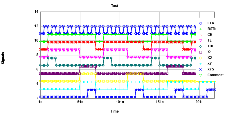
MUX simulation
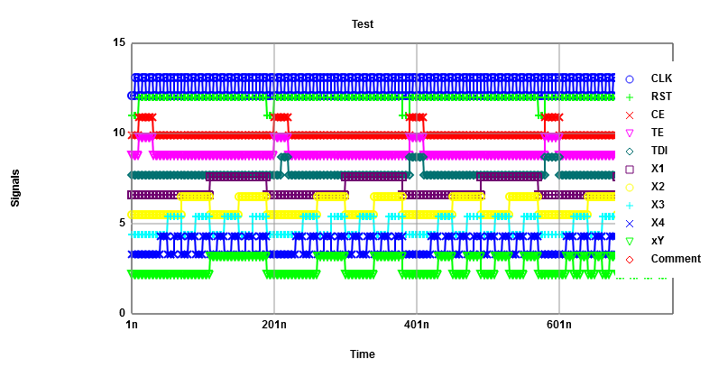
The upper image shows the waveforms of the inputs and the expected outputs as displayed by TestJS.html. The lower image is the result of the simulation with defined inputs. The inputs are x1, x2, x3, x4. Registers are set with TE and TDI using a scan operation. Before setting registers a reset is done. xY is set to the value of one of the four inputs x1 . x4. This depends on the states of the two scan cells, because they control the multiplexer.
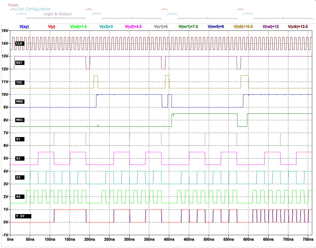
The time diagram shows the result of the simulation in LTSPICE. Here it can be seen, that depending on the values configured on MR0 and MR1, the output takes the same pattern of X1, X2, X3 or X4. It can also be seen, that there is a time delay between the expected output and the real output.
DEMUX simulation
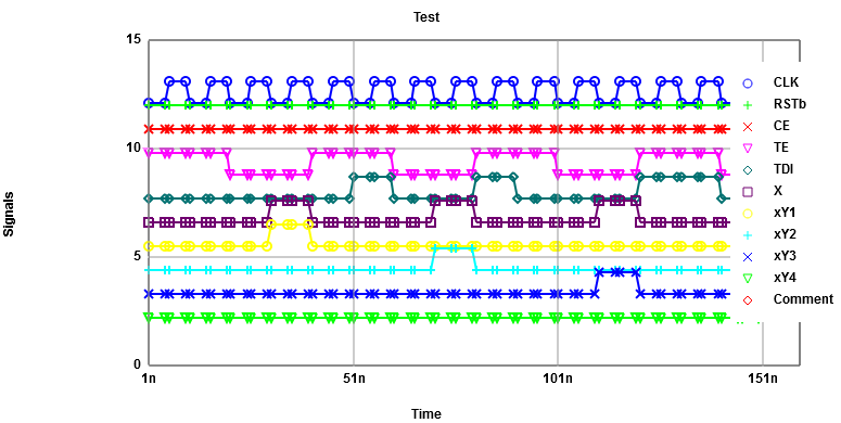
The upper image shows the waveforms of the inputs and the expected outputs generated by TestJS.html. The lower image is the result of the simulation with defined inputs. The inputs are TE, TDI and x. CE and RST were set to 1 in the command for the simulation. The outputs are given by y1, y2, y3, y4 and TDO. The input x is either fed to y1, y2, y3 or y4. This depends on the states of the two scan cells DR0 and DR1, as they control the demultiplexer. But as you can see in the waveforms of simulation this isn't a good test as we didn't test the outputs y2 and y3. The TDO is the same as the TDI signal, but delayed by two clock cycles, because there are two scan cells.

Opposite to the previous result, according to the values configured in DR0 and DR1, the input X is transmitted either to Y1, Y2, Y3 or Y4. It can also be seen that the expected output differs some period of times. As explained before in 4.4, as the output is not updated, the value it gets is random. In order to prevent this to happen, the output is leaded to an intermediate state of 0.5V. This value could be obtained in the vector generation application.
LUT simulation
Replace with good TestJS output
The upper image shows the waveforms of the inputs and the expected outputs. The lower image is the result of the simulation with defined inputs. The test vector for the inputs was generated with the test vector creation. This was copied in a text document. In excel the text document was imported and the expected outputs were added by hand. This table was inserted on the website for the test vector generation again and the waveforms with the expected outputs were generated (upper picture). It also created a LTSPICE code. This code was used for the simulation with LTSPICE. Furthermore, an additional test circuit is required for testing, where the commands for the simulation are placed.
For the simulation we chose the inputs x1, x2 and test data in (TDI). The clock (CLK) signal is created automatically by the test vector generator. The chip enable (CE), reset (RST) and test enable (TE) signals were set to 1 in the simulation command. The outputs were test data out (TDO), Y and YR.
TDO depends on TDI and on the CLK, because TDI is shifted to the next scan cells with a rising clock edge. Due to the six scan cells we got a six clock cycles delay of TDO. Y is depending on the inputs x1 and x2, because these two inputs control the multiplexer. So, Y takes the value of the output of the selected scan cell. YR is the same value as Y, but one clock cycle delayed. Therefore, YR is the value of Y of the previous clock cycle.
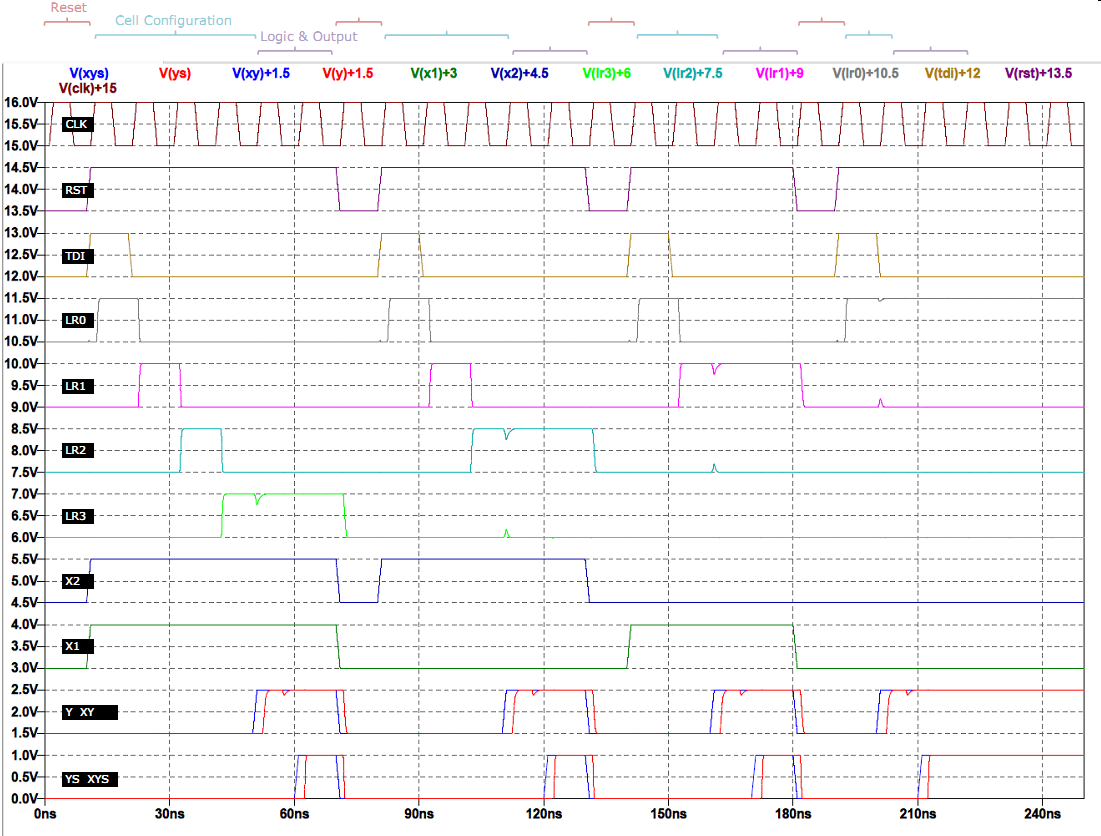
According to the values of X1 and X2, the output Y takes the value, one clock cycle later, stored in either LR0, LR1, LR2 or LR3. As well, one cycle more, the value YS updates with the value of Y. To test this block easily, all the stored values in the input registers LR0, LR1, LR2 and LR3 were set to zero, except the register to be transferred. In this way, according to the right selection of X1 and X2, the output Y and YS should be updated as well with a 1. This test was also limited due to time limits.
Propagation delay
In the third part of the lab propagation delays from input(s) to output(s) for all three blocks were performed. To provide a realistic load at the outputs as well as a realistic input waveform, inverters were connected to the appropriate inputs and outputs of the blocks. Yet another inverter was added to each of those so all previously created test vectors could be easily reused. For all measurements tpd LH indicates the propagation delay for a rising edge on the input, tpd HL for a falling edge on the input.| TMUX propagation delay | ||||
| Input | Output | # | tpd LH [ns] | tpd HL [ns] |
| X1i | Yi | 1 | 0.926 | 0.926 |
| X2i | Yi | 2 | 0.925 | 1.23 |
| X3i | Yi | 3 | 0.925 | 1.26 |
| X4i | Yi | 4 | 0.924 | - |
| TDEMUX propagation delay | ||||
| Input | Output | # | tpd LH [ns] | tpd HL [ns] |
| Xi | Y1i | 1 | 0.266 | 0.302 |
| Xi | Y2i | 2 | 0.212 | 0.243 |
| Xi | Y3i | 3 | 0.238 | 0.269 |
| Xi | Y4i | 4 | 0.185 | - |
| TLUT2 propagation delay | ||||
| Input | Output | # | Delay | tpd [ns] |
| X1i | Yinti | 1 L ! H | 1.42 | |
| X1i | Yinti | 2 H ! L | 0.490 | |
| X2i | Yinti | 3 L ! H | 1.25 | |
| X2i | Yinti | - H ! L | - | |
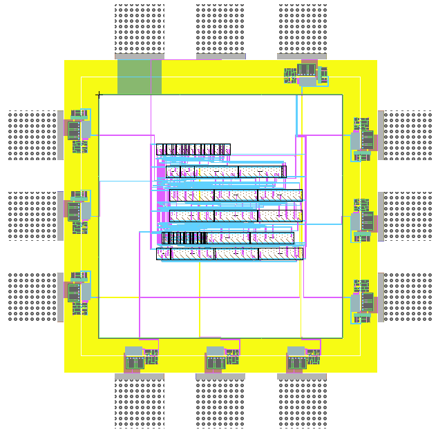
TinyFPGA and layout
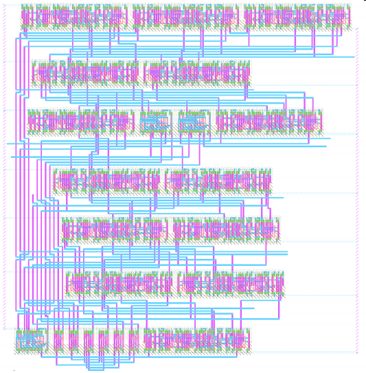
In the last part of the lab, the schematic of the Tiny FPGA was put together according to the lab's manual using the previously created blocks.As a last step the schematic was synthesized to an actual layout using Electric's silicon com- piler. After running the silicon compiler, all blocks for which a layout already existed were removed from the generated VHDL code. When trying to generate a layout from this code, an error occured indicating that the TDO signal of one of the output demultiplexers wasn't con- nected. Since we suspected that the problem might be that all of the blocks exports were cre- ated as bidirectional I/Os, all input and output signals of the "TMUX", "TDEMUX" and "TLUT2" blocks were changed accordingly. After this, the circuit could be successfully synthesized into the layout shown; the number of rows for the silicon compiler was set to 7 in order to obtain an almost rectangular layout.
Since there was no more time left, this concluded the last lab of Microelectronics.
Outlook
Time, Effort and Grading
| Topic | options | Abu | Cor | Diw | Gal | Lin | Mag | Mül | Pat | Rup | Sin | Thu | Raw | Hei | Sch |
| Topic | options | st1 | st2 | st3 | st4 | st5 | st6 | st7 | st8 | st9 | st10 | st11 | st12 | st13 | st14 |
| Introduction | Objectives, Environment, Strategy | 1 | 1 | 1 | 1 | 1 | 1 | 1 | 1 | 1 | 1 | 1 | 1 | 1 | 1 |
| MUX | schematic, text | 0.5 | 2 | 0.5 | 2 | 2 | 1 | 2 | 0.5 | 2 | 1 | 2 | 1 | 1 | 2 |
| MUX | state table, text, highlighting | 2 | 1.5 | 2 | 2 | 1 | 2 | 1.5 | 1 | 1 | 2 | 1 | 2 | 1 | |
| DEMUX | schematic, text | 0.5 | 2 | 0.5 | 2 | 2 | 1 | 2 | 0.5 | 2 | 1 | 2 | 1 | 1 | 2 |
| DEMUX | Resistors, good connection | 1.5 | 1 | 1 | 2 | 1 | 2 | 2 | 1 | 1 | |||||
| DEMUX | state table, text, highlighting | 2 | 1.5 | 2 | 2 | 1 | 2 | 1.5 | 1 | 1 | 2 | 1 | 2 | 1 | |
| LUT | schematic, text | 0.5 | 2 | 0.5 | 2 | 2 | 1 | 2 | 0.5 | 2 | 1 | 2 | 1 | 1 | 2 |
| LUT | state table, text, highlighting | 2 | 1.5 | 2 | 2 | 1 | 2 | 1.5 | 1 | 1 | 2 | 1 | 2 | 1 | |
| Test vector generation | text | 1 | 1 | 1 | 1 | 1 | 1 | 2 | 1 | ||||||
| MUX | simulation, extra label | 1 | 2 | 0.5 | 1 | 1 | 1 | 1 | 0.5 | 1 | 1 | 2 | 1 | 1 | 1 |
| DEMUX | simulation, extra label | 1 | 2 | 0.5 | 1.5 | 1.5 | 1 | 1 | 0.5 | 1 | 1 | 2 | 1 | 1 | 1 |
| LUT | simulation, extra label | 1 | 2 | 0.5 | 1.5 | 1.5 | 1 | 1 | 0.5 | 1 | 1 | 2 | 1 | 1 | 1 |
| Outlook | text | 1 | 0.5 | 1 | 1 | 1 | 1 | 0.5 | 1 | 1 | 1 | 1 | |||
| Problems | text | 1 | 1 | 1 | 1 | 1 | 1 | 1 | 1 | 1 | 1 | 1 | 1 | 1 | |
| Time efforts | time [h] | 13 | 7.5 | 13 | 9 | 9 | 17 | 13 | 13 | 17 | 21 | 20 | 18 | ||
| Pages | 27 | 17 | 11 | 19 | 19 | 20 | 18 | 7 | 10 | 20 | 47 | 9 | 10 | 10 | |
| English | no text | 1 | 1 | 1 | 1 | 1 | 1 | 1 | 1 | 1 | 1 | 0 | 1 | 1 | |
| Extra | VHDL, Matlab code | colored test table | Flow chart, IO | Flow chart, IO | AnalyzeJS output | student10 | Propagation delay, layout, Matlab | student12 | student13 | AnalyzeJS output | |||||
| Grading | Abu 3.0 Thu | Cor 1.3 | Diw 3.0 Pat |
Gal 1.3 |
Lin 1.3 | Mag 1.3 Sin | Mül 1.3 |
Pat 3.0 Diw |
Rup 1.7 Sch | Sin 1.3 Magoc |
Thu 1.0 Abu | Raw 1.3 Hei |
Hei 1.3 Raw | Sch 1.7 Rupp |
Effort
| Task | Abu | Cor | Diw | Gal | Lin | Mag | Mül | Pat | Rup | Sin | Thu | Raw | Hei | Sch | |
| Schematic | time[h] | 3 | 2.5 | 3 | 1.5 | 1.5 | 5 | 2.5 | 3 | 5 | 2.5 | 7.5 | 3 | ||
| Simulation | time[h] | 11 | 3.5 | 7 | 7.5 | 7.5 | 7 | 3.5 | 7 | 7 | 7.5 | 7.5 | 11 | ||
| Documentation | time[h] | 5 | 4 | 5 | 9 | 5 | 3.5 | ||||||||
| Debugging | time[h] | 1.5 | 2 | 5 | 2 | ||||||||||
| Delay | 3 |
Problems and Solutions
| Description | Solution |
| Tried to make the simulation of the block in the same schematic. | Create a separate schematic just for testing and invoke the block with the icon view. |
| Exports were created in the schematic of the block. Once the simulation was configured in the test schematic, the export did not appear on the list of the graphics. | The exports must also be created in the test schematic. |
| First time, the code generated for the test vectors was copied directly to the schematic in a new LTSpice code. This generated lot of error in the added line in LTSPICE simulation. | Multi-line option must be selected for the code object in order to avoid this problem. This can be done in the Edit menu -> properties -> object properties, the select the multi-line text option. |
| At the beginning, some of the blocks were working with the falling edge clock. | An updated version for "sclib" library was released, and the behavior of this was changed. |
| Using a clock definition with no time delay or 5ns delay, in some block leaded to not to catch the right input value in the registers, and therefore the logic and the expected value failed. | Use a small-time delay of 1ns, with this the register takes the value in the right cycle. |
Some facts experienced:
| Most of the times, these problems were caused by failed exports. The exports were disconnected. Could be also short circuits. The solution is: delete and redo the export or make a correction in the electric lines. |
| For combination of inputs of 2 signals, the output could be seen but in very distinct time of combination, and therefore the expected value was not in the exact time. | The combination led to another output than the expected. It is just a matter to change the expected value, as the block works with the truth table, or change the combination to obtain the right output. |
| Test vector were not easy to plan, in order to get the code for the simulation. | The functioning of the vector generator was understood, by the time it was realized that the vectors are like the clock by clock sequence, and therefore, the plan to put the right configuration had to be done first thinking by the clock and logic sequence. |
- No laboratory during holidays
- the long time, that we needed to understand how the test-vector generator works
- the time for the discussion how the test vectors should be created
- the time for debugging
Summary and Discussion
Accomplishments:- A tool can convert a truth/state table in a LTSPICE/IRSIM simulation file.
- Benefits of an automated toolchain were experienced.
- A circuit was placed in an IO-Pad frame
- Test and scan cell operation was simulated.
- A basic layout renderer for HTML5 was created.
- Test vector creation was improved.
- Discovery of IRSIM technology files:
300nm
First try modification for 50nm
- Provide a working IO-Pad simulation
- Make real IO-Pads
- Provide working IRSIM simulations with expected output
- Provide Chip id and test structures.
What is the relationship between number of pins, switch matrix and LUTs?
What would be the optimum number of global lines, inputs/outputs for switch matrix and LUTs?
Implement a state machine or truth table in FPGA.