
Open Laboratory 2021: Cell optimization
Joerg VollrathLaboratory Instructions
In this laboratory cells from sclib.jelib are optimized and characterized.
| Nr | Matrikelnummer, Name | Cell (sclib) |
| 1 | *****916, A | LUT22 |
| 2 | *****430, A | LUT23 |
| 3 | *****708, A | LUT24 |
| 4 | *****711, A | LUT27 |
| 5 | *****407, B | LUT28 |
| 6 | *****399, H | LUT2B |
| 7 | *****729, K | LUT2D |
| 8 | *****215, K | LUT2E |
| 9 | *****461, Ö | LUT22 |
| 10 | *****414, R | LUT23 |
| 11 | *****995, R | LUT24 |
| 12 | *****727, R | LUT27 |
| 13 | *****104, S | LUT28 |
| 14 | *****305, S | LUT2B |
| 15 | *****443, T | LUT2D |
| 16 | *****807, A | LUT2E |
Cell Layout Optimization
Create a new library with the cell name.
Place the original cell in.
Place a driving and load inverter in the library.
Create an optimized cell.
Create a test cell.
Optimize the cell layout and compare old and new design.
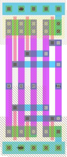
Example: Optimized cells Switch2a.jelib LUT21 as pictured above
Optimization rules
- Unit transistors:
PFET W=10 L=2
NFET W=7 L=2 - Exports M2-M1 contact in the center where the n-well meets the p-substrat.
- Exports have same grid as the VDD nwell, gnd p-substrat contacts.
- Straight polysilicon lines.
- Vertical M2 lines, horizontal M1 lines.
Characterization
Characterize functionality (truth table), delay times and power consumption with realistic source and load of the old and new cell with and without parasitics.
Deliverables
Explanation what you changed and why.
DRC no errors.
NCC no errors.
Layout
Delay times.
Power consumption.
Document your laboratory in a pdf document with a name of <Year>_Cell_ <name>.pdf and a <CellName>_<Initials>.jelib and send it to joerg.vollrath@hs-kempten.de.
Submission is due xx.xx.2021.