Open Laboratory 2021: Multiplier
Joerg VollrathLaboratory Instructions
Starting with a 2x2 Multiplier design of a 3x3 and 4x4 multiplier are explored.
The output is buffered with a sacn register.
Pads are attached.
Simulate pads.
Video of Multiplier (17.05.2021)
|
Länge: 0:54:00 |
0:0:0 Multiplier 0:2:14 Example 2 2 bit numbers 0:6:10 Design options 0:11:59 Inputs and outputs, equations 0:16:9 Add2 operation LUT26, LUT28 0:18:59 LUT26 naming convention 0:22:59 Start library multiplier 0:23:46 Schematic 0:30:39 Make icon 0:32:14 Hooking up the subcircuits 0:36:44 Simulation 0:39:39 SPICE text 0:41:1 Pulse statements 0:42:14 Simulate SPICE 1:18:4 Setting up waveform display 0:44:12 Check output 0:46:34 Generate reference output 0:48:14 Tool silicon compiler 0:50:34 Change text size 0:51:44 LTSPICE layout simulation |
Video of Multiplier (31.05.2021)
|
Länge: 0:50:41 |
0:0:0 Welcome 0:10:5 Questions 0:10:5 Preferences Silicon Compiler 0:12:22 Simulation layout 0:14:10 Reference signals for simulation 0:17:14 TestJS: Truth table to LTSPICE PWL statement 0:21:0 Propagation delay with reference signals 0:23:50 Testing and vectors 0:25:40 Silicon Compiler multiplier 0:27:40 Layout and Exports of test cell 0:34:30 Test signal genration 0:35:25 Generate LTSPICE waveform 0:36:25 generate signals 0:39:19 Connecting a cell for testing 0:43:5 Checking Exports 0:45:29 Simulation results |
Video of Multiplier (7.06.2021)
|
Länge: 0:50:41 |
0:0:0 LTSPICE schematic no AD, AS, PD, PS 0:0:0 Schematic -> VHDL -> silicon compiler 0:2:21 Reusable addx 0:2:51 Silicon compiler option rows. 0:4:51 VHDL multiplier start 0:6:48 Paste VHDL Text and replace STD_LOGIC with Bit 0:9:1 Check working Silicon compiler change VHDL cell name 0:10:56 Ports modification in and out 0:13:14 LUT modification, more MUX 0:16:24 Syntax check with silicon compiler 0:16:24 LUT2 requirement analysis 0:18:32 Identifying output codes 0:23:20 components LUT2.. 0:24:49 Adding y4.. 0:26:4 MUX modification 0:27:42 Summary of steps 0:30:24 LTSPICE text and simulation 0:32:2 Simulation configuration and result 0:35:34 Discussion VHDL text versus schematic 0:36:25 0 0:36:25 Last laboratory: built addx 0:38:5 0 |
Video of Multiplier (14.06.2021)
|
Länge: 0:50:41 |
0:0:10 Evaluation 0:0:10 Multiplier 0:0:51 LTSPICE longest delay 0:2:32 LTSPICE netlist 0:5:37 net@16 net@19, net@11 0:10:10 Control panel, Save Defaults activate subcircuit voltages 0:12:36 Add signals net@16 0:17:2 W/L change not usefull 0:18:41 Schematic 0:22:10 IRSIM switch level simulator |
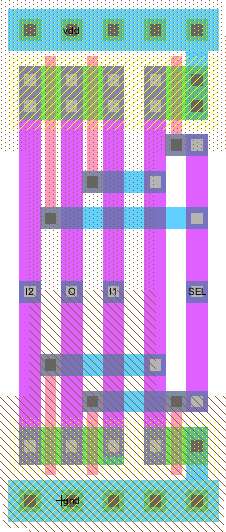
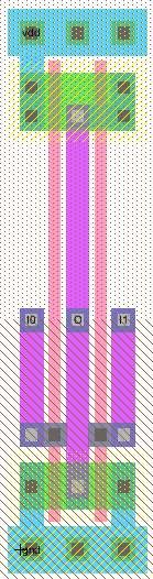
2x2 Multiplier
2 positive 2 bit numbers.Function
| A1 | A0 | * | B1 | B0 | |
| 1 | 1 | * | 1 | 0 | |
| 0 | 0 | B0 = 0, result 00 | |||
| 1 | 1 | B1 = 1, result A | |||
| Carry | |||||
| 1 | 1 | 0 | Result R |
Possible Solutions
- Boolean function:
Schematic
Behavioral VHDL, Webpack - Lookup table:
VHDL
LUT2, MUX
Boolean Function
| R0 = A0 * B0 | LUT28 |
(R2C, R2) = add2 (B1 * A1 , R1C)
R3 = R2C
add2:
| A | B | R | C |
| 0 | 0 | 0 | 0 |
| 0 | 1 | 1 | 0 |
| 1 | 0 | 1 | 0 |
| 1 | 1 | 0 | 1 |
R = (/A * B) + (A * /B)
R: LUT26
C = A * B
C: LUT28
Lookup Table
| A1 | A0 | B1 | B0 | R3 | R2 | R1 | R0 |
| 0 | 0 | 0 | 0 | 0 | 0 | 0 | 0 |
| 0 | 0 | 0 | 1 | 0 | 0 | 0 | 0 |
| 0 | 0 | 1 | 0 | 0 | 0 | 0 | 0 |
| 0 | 0 | 1 | 1 | 0 | 0 | 0 | 0 |
| 0 | 1 | 0 | 0 | 0 | 0 | 0 | 0 |
| 0 | 1 | 0 | 1 | 0 | 0 | 0 | 1 |
| 0 | 1 | 1 | 0 | 0 | 0 | 1 | 0 |
| 0 | 1 | 1 | 1 | 0 | 0 | 1 | 1 |
| 1 | 0 | 0 | 0 | 0 | 0 | 0 | 0 |
| 1 | 0 | 0 | 1 | 0 | 0 | 1 | 0 |
| 1 | 0 | 1 | 0 | 0 | 1 | 0 | 0 |
| 1 | 0 | 1 | 1 | 0 | 1 | 1 | 0 |
| 1 | 1 | 0 | 0 | 0 | 0 | 0 | 0 |
| 1 | 1 | 0 | 1 | 0 | 0 | 1 | 1 |
| 1 | 1 | 1 | 0 | 0 | 1 | 1 | 0 |
| 1 | 1 | 1 | 1 | 1 | 0 | 0 | 1 |
Tool zur Erzeugung der LTSPICE Waveform TestJS
A1,A0,B1,B0;xR3,xR2,xR1,xR0,COMMENT
0,0,0,0;0,0,0,0; 0*0=0
0,0,0,1;0,0,0,0; 0*1=0
0,0,1,0;0,0,0,0; 0*2=0
0,0,1,1;0,0,0,0; 0*3=0
0,1,0,0;0,0,0,0; 1*0=0
0,1,0,1;0,0,0,1; 1*1=1
0,1,1,0;0,0,1,0; 1*2=2
0,1,1,1;0,0,1,1; 1*3=3
1,0,0,0;0,0,0,0; 2*0=0
1,0,0,1;0,0,1,0; 2*1=2
1,0,1,0;0,1,0,0; 2*2=4
1,0,1,1;0,1,1,0; 2*3=6
1,1,0,0;0,0,0,0; 3*0=0
1,1,0,1;0,0,1,1; 3*1=3
1,1,1,0;0,1,1,0; 3*2=6
1,1,1,1;1,0,0,1; 3*3=9
Design with Lookup Table (VHDL, LUT2, MUX)
Start with structural example from lecture and modify:
entity LUT4_0DF0 is port( I0,I1,I2,I3: in STD_LOGIC;O: out STD_LOGIC);
end LUT4_0DF0;

architecture LUT4_0DF0_BODY of LUT4_0DF0 is
  component LUT20 port ( I0,I1 : in STD_LOGIC;O: out STD_LOGIC); end component;
  component LUT2D port ( I0,I1 : in STD_LOGIC;O: out STD_LOGIC); end component;
  component LUT2F port ( I0,I1 : in STD_LOGIC;O: out STD_LOGIC); end component;
  component MUX4 port(I0,I1,I2,I3,I4,I5 : in STD_LOGIC;O: out STD_LOGIC); end component;

  signal y1,y2,y3,y4,O2 : STD_LOGIC ;

begin
  LUT2_1: LUT20 port map (I0,I1,Y1);
  LUT2_2: LUT2F port map (I0,I1,Y2);
  LUT2_3: LUT2D port map (I0,I1,Y3);
  LUT2_4: LUT20 port map (I0,I1,Y4);
  MUX0: MUX4 port map (Y1,Y2,Y3,Y4,I2,I3,O);
end LUT4_0DF0_BODY;
Change VHDL code.1. Replace STD_Logic with Bit
2. Change entity name from LUT4_0DF0 to multiplier2x2vhdl
3. Check with Silicon compiler operation correct syntax
4. Change input (I0,I1,I2,I3) to (B1, B0, A1, A0), outputs (O) to (R3, R2, R1, R0)
5. Add multiplier instances for R0, R1, R2, R3
6. Check with Silicon compiler operation correct syntax
7. Get needed LUTs and combinations for R3, R2, R1, R0 from truth table
8. Adjust components to needed LUT2xs
9. Adjust instances of LUT2_x and signals yx
10. Adjust MUX instances with correct pattern
11. Check with Silicon compiler operation correct syntax
12. Add LTSPICE simulation commands to layout
13. Simulate with LTSPICE
entity multiply2x2vhdl is port( A1,A0,B1,B0: in Bit;R3,R2,R1,R0: out Bit);
end multiply2x2vhdl;

architecture multiply2x2vhdl_BODY of multiply2x2vhdl is
      component LUT20 port ( I0,I1 : in Bit;O: out Bit); end component;
      component LUT28 port ( I0,I1 : in Bit;O: out Bit); end component;
      component LUT2C port ( I0,I1 : in Bit;O: out Bit); end component;
      component LUT24 port ( I0,I1 : in Bit;O: out Bit); end component;
      component LUT2A port ( I0,I1 : in Bit;O: out Bit); end component;
      component LUT26 port ( I0,I1 : in Bit;O: out Bit); end component;
      component MUX4 port(I0,I1,I2,I3,I4,I5 : in Bit;O: out Bit); end component;

      signal y1,y2,y3,y4,y5,y6: Bit ;
--            Y 4321
-- R3 = 0x8000
-- R2 = 0x4C00
-- R1 = 0x6AC0
-- R0 = 0xA0A0
begin
      LUT2_1: LUT20 port map (B0,B1,Y1);
      LUT2_2: LUT28 port map (B0,B1,Y2);
      LUT2_3: LUT2C port map (B0,B1,Y3);
      LUT2_4: LUT24 port map (B0,B1,Y4);
      LUT2_5: LUT2A port map (B0,B1,Y5);
      LUT2_6: LUT26 port map (B0,B1,Y6);
--                                            Y   1   2   3   4
      MUX3: MUX4 port map (Y1,Y1,Y1,Y2,A0,A1,R3);
      MUX2: MUX4 port map (Y1,Y1,Y3,Y4,A0,A1,R2);
      MUX1: MUX4 port map (Y1,Y3,Y5,Y6,A0,A1,R1);
      MUX0: MUX4 port map (Y1,Y5,Y1,Y5,A0,A1,R0);
end multiply2x2vhdl_BODY;
Design with reusable block Addx
Input; Bn, Am, Si, Ci
Output:Co, S
Function: Co S = Bn*An + Si + Ci

Bn Am Si Ci | S Co
 0  0  0  0 | 0  0
 0  0  0  1 | 1  0
 0  0  1  0 | 1  0
 0  0  1  1 | 0  1
 0  1  0  0 | 0  0
 0  1  0  1 | 1  0
 0  1  1  0 | 1  0
 0  1  1  1 | 0  1
 1  0  0  0 | 0  0
 1  0  0  1 | 1  0
 1  0  1  0 | 1  0
 1  0  1  1 | 0  1
 1  1  0  0 | 1  0
 1  1  0  1 | 0  1
 1  1  1  0 | 0  1
 1  1  1  1 | 1  1
Co = (S1*C1) + (Bn*Am*(Si*/Ci+/Si+Ci))
Design this block addx and a 2 x 2 multiplier using schematic oder VHDL and simulate it.
Design options
Design for:
- Automation
- Manufacturing
- Test
- Performance
- Diagnosis
- Reuse
Compare the designs of the multipliers
What is the longest delay path?
How easy is it to design a 3x3, 4x4 multiplier?
What about effort?
What about automation?
What about area?
Characterization
Characterize functionality (truth table), delay times, area and power consumption with realistic source and load of the old and new cell with parasitics.
Discuss benefits and drawbacks of different design styles.
Deliverables
Document your laboratory in a pdf document with a name of <Year>_Multiply_ <name>.pdf and a <Multiply>_<Initials>.jelib and send it to joerg.vollrath@hs-kempten.de.
Submission is due 09.07.2021.
Adding Pad Frame
Use and load the library Pads4u.jelib.
Keep multiplier as the "Current Library".
Download file padsMultiplier2x2.arr and save it to your local directory.
Modify the file according to the inputs and outputs.
Insert in the line core your top level circuit layout name.
Names are case sensitiv.
Try to make a square pad frame:
Tools - Generation - Pad Frame Generator: select file padsMultiplier2x2.arr
Tools - Routing - Sea of Gates Route
Simulating bigger circuits with IRSIM
LTSPICE has some limits of the number of transistors it can simulate in a reasonable amount of time.
It is possible to transfer the structural VHDL code to a FPGA design suite and simulate it.
Electric has built in a switch level simulator IRSIM.
It is very user unfriendly to operate.
The HTMLpage for LTSPICE stimuli provides also IRSIM commands which can be saved in a <name>.cmd file.
To display reference signals the cell TestSignal can be used and appropriate Exports created.
IRSIM is started with: Tools, Simulation(Built-in), IRSIM Simulate current cell
Stimuli are loaded with: Tools, Simulation(Built-in), Restore stimuly from disk
Window, Fill window displays all signals
At the top of the subwindow the height of the rows can be changed.
Window Zoom in is used to zoom in and be able to measure delays with cursors (Center the cursors).
Grabbing the time display scrolls the display left and right.
A parameter file scmos0.3.prm built into Electric is used.