A DRAM memory cell has a size of 8F2. 55% of chip area can be used
for memory cells, 45% of chip area is used for periphery circuits and IO pads.
How big is a 1GBit chip in 70nm technology?
How many chips fit on a wafer with 200mm diameter?
How many good chips do you get with 70% yield?
What is the defect density for this yield?
SS 2018 Problem 2: VHDL
entity ThisCircuit is port (
        INSIGNAL : in std_logic_vector (3 downto 0);
        OUTSIGNAL: out std_logic );
end ThisCircuit;

architecture ThisCircuit_BEHAVE of ThisCircuit is
signal  a: std_logic;
begin
 a <= INSIGNAL(2) or INSIGNAL(1) ;
 OUTSIGNAL <= INSIGNAL(3) and  a and INSIGNAL(0);
end ThisCircuit_BEHAVE;
Draw a schematic described by this VHDL code.
Make a truth table of this circuit?
How many vectors do you need to test the circuit?
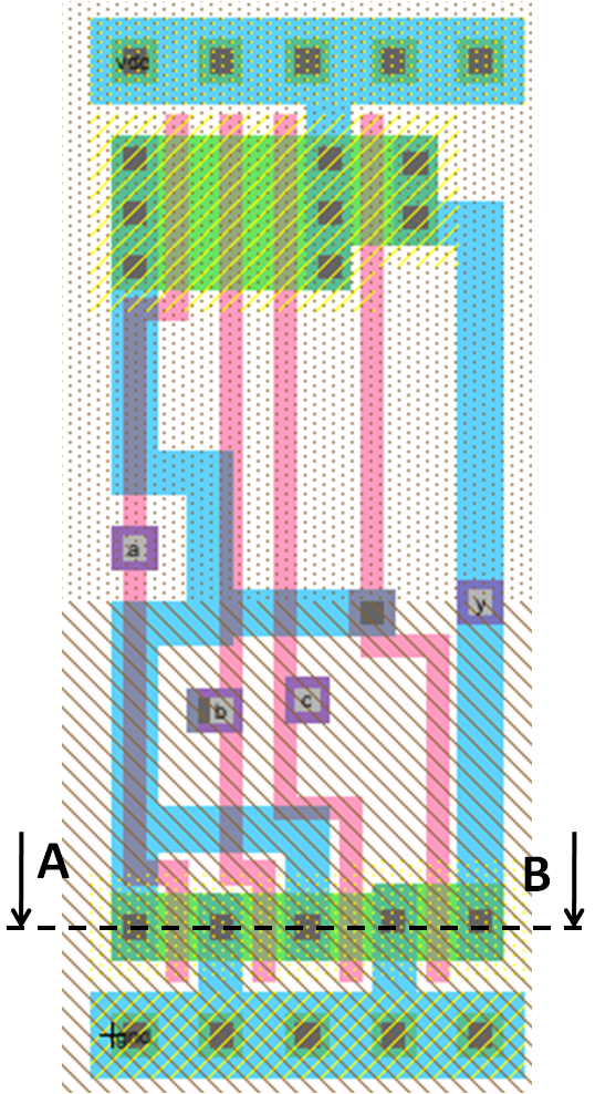
SS 2018 Problem 3: Circuit and Layout Analysis
Calculate the input capacitance of the circuit on the right. The
transistor has minimum length in 1µm technology.
Technology
Rn
Rp
Scale factor
Cox=C'oxWL·(scale)2
1µm (long-channel)
15kL/W
15kL/W
1µm
(1.75fF)·WL
Calculate the contact resistance of the drain and
source contacts, if a single contact has a resistance of 10Ω.
A capacitance of 50pF is connected to the output.
Calculate the propagation delays and rise and fall time of the
output.
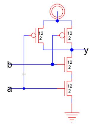
SS 2018 Problem 4: Truth table AOI circuit
Make a truth table for the circuit on the right.
How do you have to resize the transistors for equal delay to an inverter with a PFET W/L of 12/2 and NFET W/L of 6/2?
Give a boolean equation for the circuit.
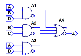
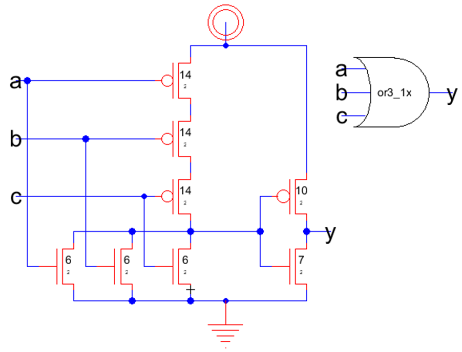
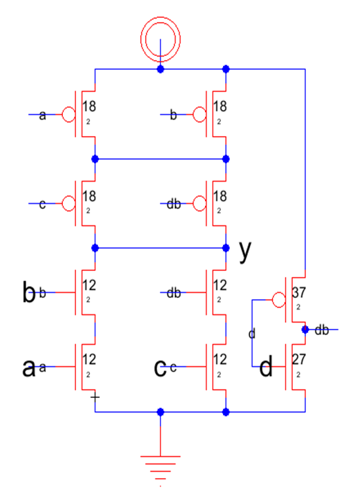
SS 2018 Problem 5: Circuit
Describe the input and outputs and the function of the circuit shown in the
schematic. What kind of circuit is it?
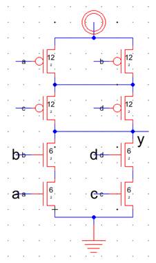
SS 2018 Problem 6: SPICE
This is the SPICE code of a netlist of a logic circuit with the input a and b and the
output y.
*** TOP LEVEL CELL:
Mnmos@0 y a 0 0 N L=0.1U W=0.4U
Mnmos@1 y b 0 0 N L=0.1U W=0.4U
Mpmos@0 net@9 b y vdd P L=0.1U W=0.8U
Mpmos@1 vdd a net@9 vdd P L=0.1U W=0.8U
VD1 vdd 0 DC 1.2
Va a 0 PULSE(0 1.2 5n 1n 1n 4n 10n 20)
Vb b 0 PULSE(0 1.2 12.5n 1n 1n 9n 20n 20)
.include cmosedu_models.txt
.tran 0 25n 0 0.01n
.END
Draw a schematic of this circuit?
What is the operating voltage?
Draw a timing diagram of the signals a, b and y.
Why do you need the file cmosedu_models.txt?
SS 2019 HKE Examination Microelectronics
SS 2019 1. Problem: Manufacturing
A wafer with 300mm diameter has 1200 Chips.
The contact yield is 98% and there are 1035 functional pass chips.
What is the total yield and the relative functional yield? (2 points)
Calculate the defect density. (2 points)
What would be the total yield, if the chips would have half the area? (2 points)
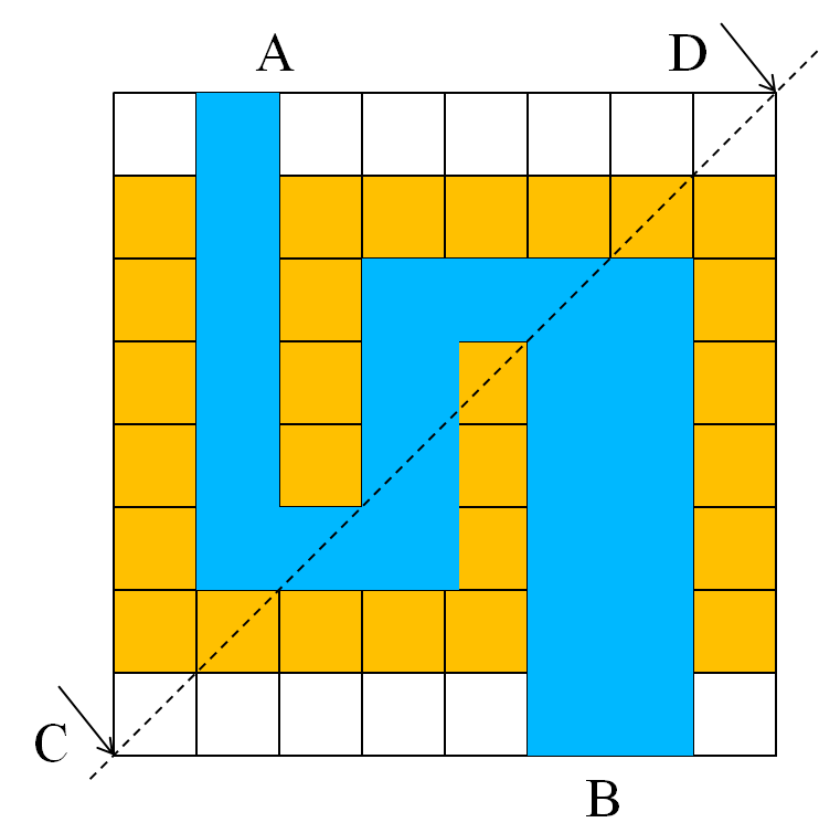
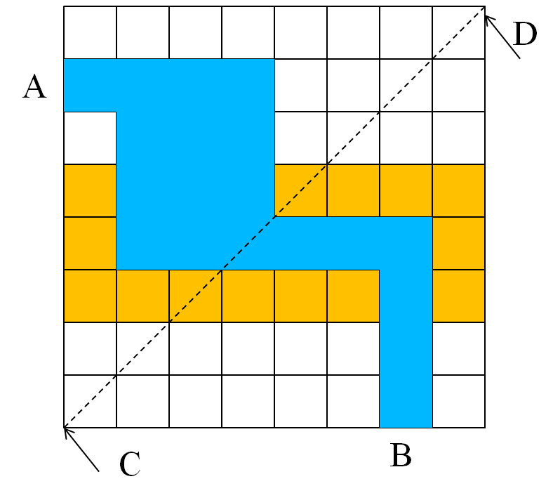
A top view of a metal line in a 50nm process running from A to B is shown crossing a polysilicon line,
which runs from left to right. The metal sheet resistance is Rsquare = 0.2 Ω/square.
Plate capacitance is 40 aF/µm2 and fringe capacitance is 90 aF/µm.
1. Calculate the capacitance between the metal line (blue) and the polysilicon line (yellow).(3 points)
2. Calculate the resistance from A to B? (1 points)
3. Calculate the voltage drop on the line if a current of 30µA is flowing.
(1 point)
4. Draw a cross section from points C to D (4 points)
Make a truth table for the following circuit: (4 points)
C
B
A
Y
Draw a transistor schematic with the estimated W/L ratio of the transistors. (6 points)
Each contact has a resistance of 20Ω. What is the minimum and maximum contact
resistance of the source drain contacts of the transistors? (3 points)
Draw a cross section along the line from A to B (5 points)
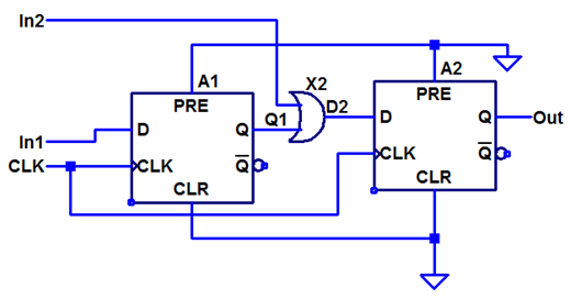
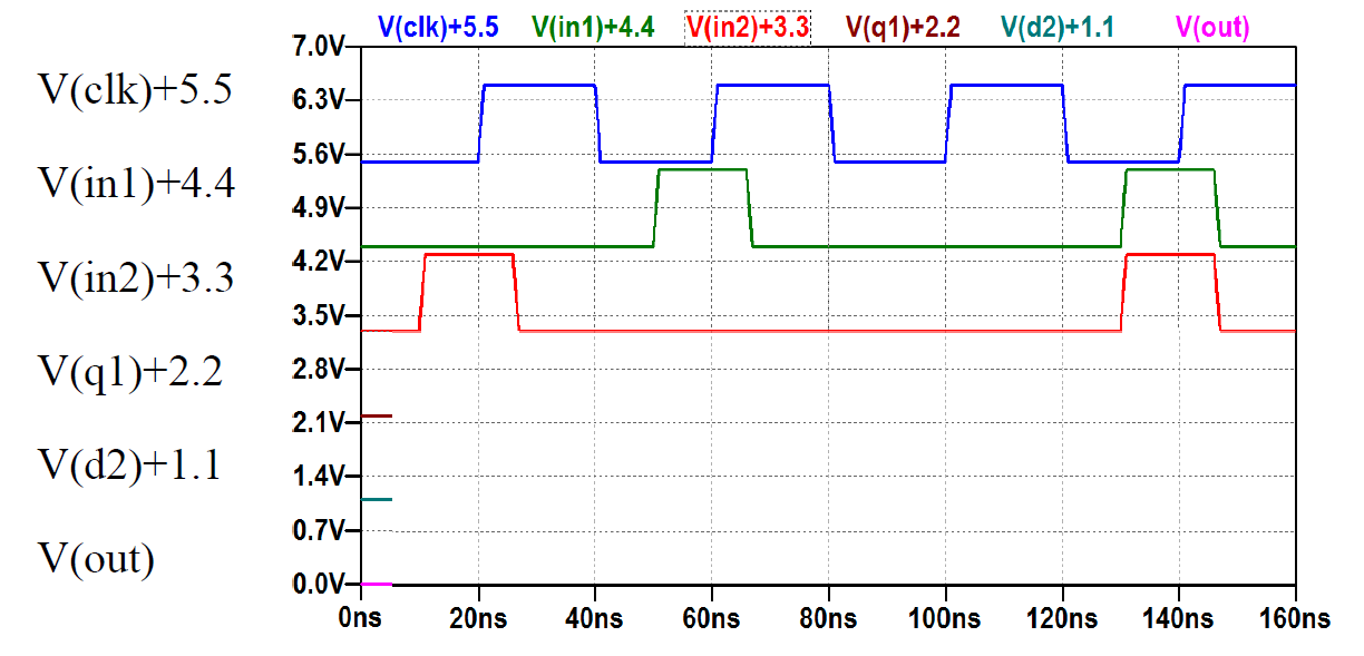
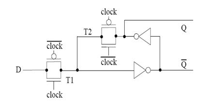
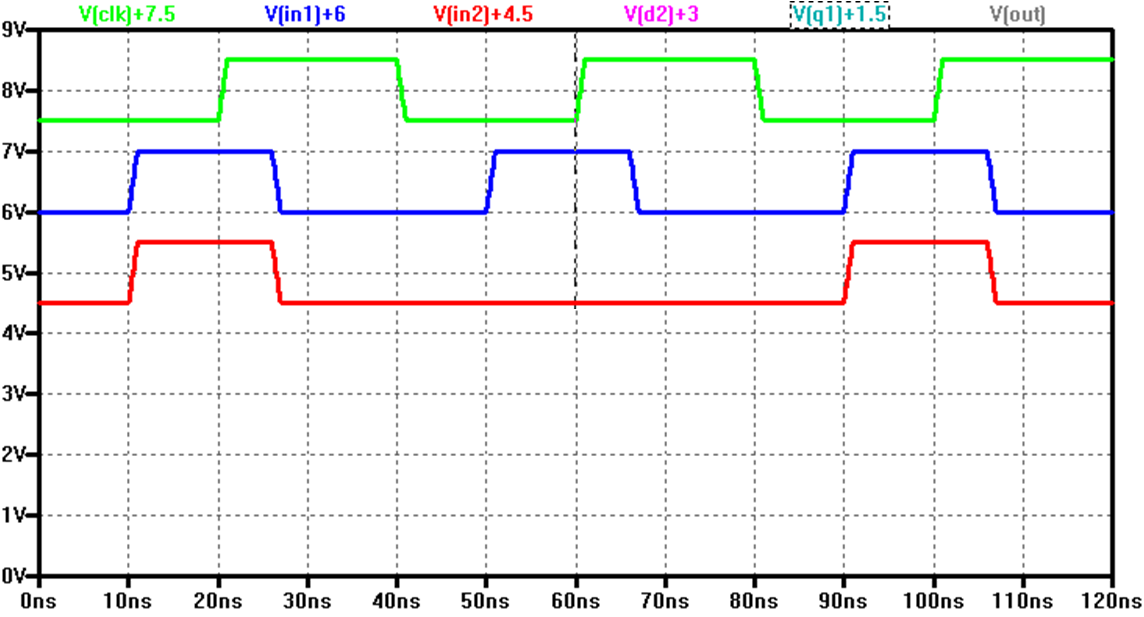
SS 2019 5. Problem: Circuit Analysis
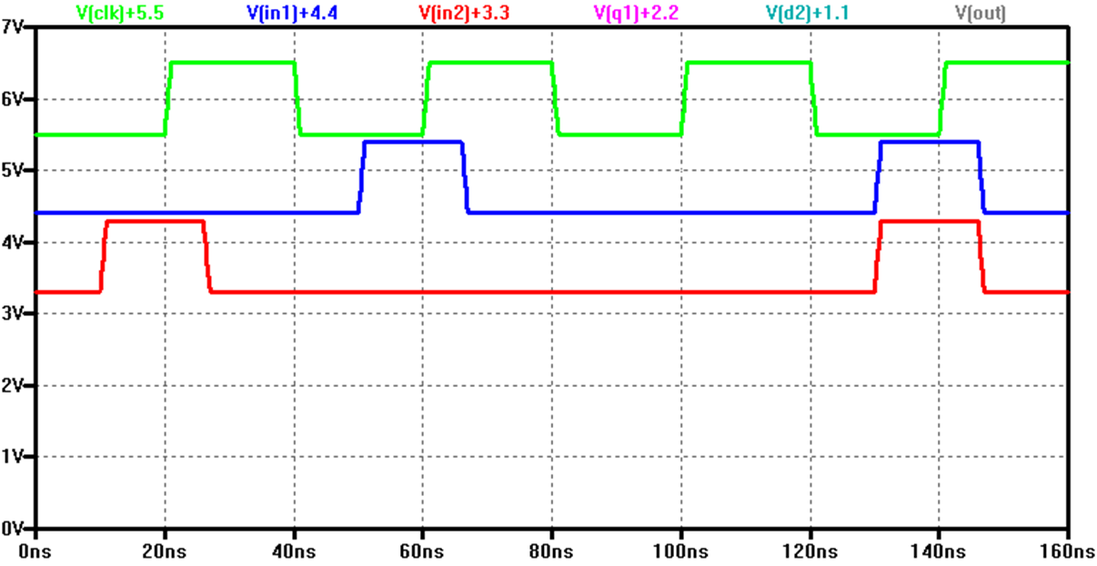
5.1 Draw the output response of nodes d2+3.0, q1+1.5 and Out. (6 points)
5.2 What are the setup and hold times? (4 points)
Tsetup= 10ns, 30ns
tHold=10ns, 30ns
SS 2019 6. Problem: SPICE netlist
* Testcell
Mnmos1 0 Y 0 0 NX L=0.1U W=2U
Mpmos1 Vdd Y Vdd Vdd PY L=0.1U W=3U
Mnmos0 Y Vdd A 0 NX L=0.5U W=4.0U
V1 A 0 SINE(0.5 0.5 50k) AC 1
VD1 vdd 0 DC 0.9
.include cmosedu_models.txt
.ac dec 10 100k 1G
.backanno
.end
1. What simulation is done with this SPICE code?
Make a schematic, describe the circuit, signals and simulation. (8 points)
2. How many transistors are implemented, what are the dimensions
and what is the transistor model name? (3 points)
3. What is the operating voltage? (1 point)
4. Draw V(a) and V(Y) of this circuit for this simulation.
Label the axis and important measurement points.
Discuss the curve. (4 points)
An AC simulation is done from 100kHz to 1GHz.
Mpmos1 and Mnmos1 are connected as capacitors as a load to a pass gate Mnmos0.
Voltage source VD1 is supplying an AC and sine stimulus with amplitude 0.5V and offset 0.5V to the circuit.
2. There are 3 transistors.
Mnmos0 W=4um, L=0.5um model NX (3)
2.3 VDD=0.9V
2.4 Just copy the spice text into LTSPICE or save as .asc file and simulate.
SS 2019 7. Problem
7.1 How can you control the gain of an amplifier? (2 points)
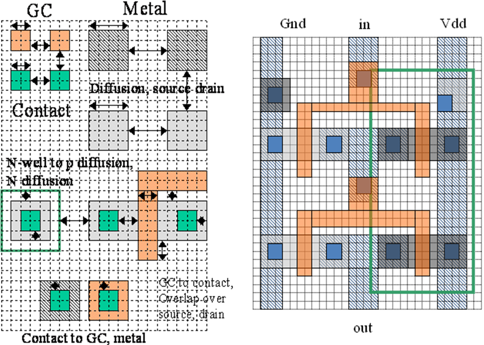
7.2 What is a stick diagram and why do you use it? (5 points)
7.3 What is a wired Or Fault model? (1 points)
7.4 What is electromigration and how do you prevent it? (4 points)
7.1:
A feedback loop can be implemented with external resistors.
A load resistance can degrade the output resistance and limit the gain.
7.2:
A stick diagram helps you to plan and draw a layout.
Wires are represented as blue and violet lines, contacts as black crosses and
transistors by crossing lines of red polysilicon and green S/D diffusion (n,p regions).
It is easier to draw only wires instead of rectangles.
Color coding helps with identifying parts and avoiding shorts.
7.3:
A fault between 2 lines is modeled as an OR Gate.
7.4:
Electromigration occurs at high currents in a metal line
where material is moved by the flowing high current. It can cause opens.
Reducing the current density with wide metal lines prevents electromigration.
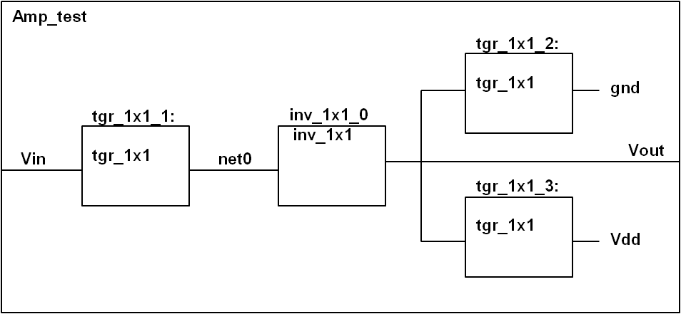
SS 2019 8. Problem: VHDL
Draw a schematic block diagram of the VHDL code. (8 points)
Label the nets and instances.
entity Amp_test is port(Vin: in BIT; Vout: out BIT);
  end Amp_test;

architecture Amp_test_BODY of Amp_test is
  component inv_1x1 port(a: in BIT; y: out BIT);
    end component;
  component tgr_1x1 port(x: in BIT; y: out BIT);
    end component;
begin
  inv_1x1_0: inv_1x1 port map(net_0, Vout);
  tgr_1x1_1: tgr_1x1 port map(Vin, net_0);
  tgr_1x1_2: tgr_1x1 port map(Vout, gnd);
  tgr_1x1_3: tgr_1x1 port map(Vout, vdd);
end Amp_test_BODY;
SS 2020 HKE Examination Microelectronics
SS 2020 Problem 1
1.1: Identify the DRAM cell types shown in the schematic (2 points).
____ SRAM
____ DRAM
____ Flash
1.2: Give the main differences between a SRAM, DRAM,
and Flash memory cell (5 points)
SS 2020 Problem 2
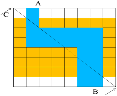
Given are the following design rules and a circuit layout.
Why are design rules needed? (2 points)
Draw the schematic of the layout below. Mark all design violations in
the layout. (5 points)
What is the width and the length of the transistors. The smallest
feature size in this process is 0.5 µm. (1 point)
Design Rules
Layout
Problem 3
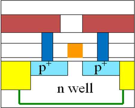
Label the different regions (Gate, Drain, Source,
Isolation, Polysilicon, Metal) in the shown cross section of a transistor.
What type of transistor is it? (5 points)
SS 2020 Problem 4:
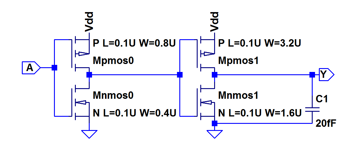
Calculate the delay and rise and fall time of the output for a rising
and falling output using the following properties. (6 points)
Calculate the input capacitance of the circuit. (2 points)
Calculate the resistance of a polysilicon line with length L. (2 points)
If the line resistance is too high, what can you do to lower the
resistance? (2 points)
Calculate the capacitance between the 2 lines. (3 points)
SS 2020 Problem 6:
Make a truth table for the following circuit.
Which Boolean function is it? (4 points)
A
B
C
Y
SS 2020 Problem 7:
Make a truth table and draw a schematic for the
following logic AOI function. Size the transistors with minimum size to achieve
a maximum delay like a inverter with PFET(15/1) and NFET(5/1).
(8 points)
\( Z = \overline{ (AB)+C+D} \)
A
B
C
D
Z
SS 2020 Problem 8:
Calculate the maximum number of chips with 150mm2 area which
fit on a 300mm wafer. (3 points)
There is 1 defect per 600mm2. How many chips will fail? (1
point)
During test of all chips 38 chips are bad. What is the yield? What is
the fault coverage? (4 points)
Is this a good fault coverage? (2 points)
What is the difference between a defect and a fault? (2 points)
SS 2021 HKE Examination Microelectronics
SS 2021 Problem 1:
A CPU with 50 Million Transistors needs 100F2 per transistor.
How big is the chip in 90nm technology? (2 points)
How many chips fit on a wafer with 300mm diameter? (3 points)
What defect density do you need to get a yield of 65%? (4 points).
How many more good chips do you get with the same defect density using a
70nm technology? (4 points).
SS 2021 Problem 2:
Make a truth table for this VHDL code. (8 points)
entity ThisCircuit is port (
  op : in STD_LOGIC_VECTOR (1 downto 0);
  vin1,vin2 : in STD_LOGIC;
  vout : out STD_LOGIC);
end ThisCircuit;

architecture Behavioral of ThisCircuit is
  signal acc:STD_LOGIC;
begin
  PROCESS (op)
  BEGIN
    CASE op IS
      WHEN "00" => acc<= '0';
      WHEN "01" => acc<= vin1 or vin2;
      WHEN "10" => acc<= vin1 xor vin2;
      WHEN "11" => acc<= vin1 and vin2;
      WHEN OTHERS => acc<='0';
    END CASE;
  END PROCESS;
  vout <= acc;
end Behavioral;
Draw a timing diagram of the signals op, vin1, vin2 and vout of
this circuit for the following stimulus. ( 6 points)
constant Tp : time := 50 ns;
stim_proc: process
begin
  op <= "00"; vin1 <='0'; vin2 <='1'; wait for Tp;
  op <= "01"; vin1 <='1'; vin2 <='0'; wait for Tp;
  op <= "10"; vin1 <='0'; vin2 <='0'; wait for Tp;
  op <= "11"; vin1 <='1'; vin2 <='0'; wait for Tp;
  op <= "11"; vin1 <='1'; vin2 <='1'; wait for Tp;
end process;
SS 2021 Problem 3: Test
Why do you have to test integrated circuits? (2 points)
Give an electrical model for a transition delay fault. (2 points)
Give an electrical model for a stuck at ´1` fault. (2 points)
What is a scan chain? What signals do you need and what is their purpose? How
does a scan chain operate? What is the benefit and drawback of a scan chain?
(12 points)
SS 2021 Problem 4:
Calculate the minimum and maximum propagation delay for the circuit
below, when a 10pF Capacitance is connected to the output. (4 points)
Calculate the maximum input capacitance of the circuit. (3 points)
What would be the W/L ratio of the transistors to optimize the circuit
for minimum power consumption? Why is the power consumption lower? (4
points)
What would be the W/L ratio of the transistors to optimize the circuit
to have a delay equal to an inverter with a NFET W/L 2/2 and PFET W/L 6/2?
(4 points)
Technology
Rn
Rp
Scale factor
Cox=C'oxWL·(scale)2
1µm (long-channel)
15kL/W
45kL/W
1µm
(1.75fF)·WL
The general equation for the propagation delay time is:
t = 0.7 R C
R is the resitance of the NFET or PFET.
C is the total capacitance at the output.
NFETs are in series:
\( R_{N} = 2 * R_{N} \frac{2}{12} = 15 k\Omega \frac{1}{3}= 5 k\Omega \)
PFETs can be activated both or only one:
\( R_{Pmin} = \frac{R_{P}}{2} \frac{2}{12} = 45 k\Omega \frac{1}{12}= 3.75 k\Omega \)
\( R_{Pmax} = R_{P} \frac{2}{12} = 45 k\Omega \frac{1}{6}= 7.5 k\Omega \)
\( C = C_{outN} + C_{outP0} + C_{outP1} + C_{1} \)
The output capacitance of an inverter is:
\( C_{out} = C_{ox} \)
Delay is an estimation with Cox/2 between gate and drain and with Cox/2 between gate and source.
A propagation delay can be observed if an inout signal change leads to an output signal change.
For a NAND gate the following switching cases are relevant:
Coxpa is the capacitance of the PFET (p) for input a (a).
Rpa is the on resistance of the PFET for input a.
If input is changing from 0 to 1 and output changes from 1 to 0 a capacitance Cox/2
between input and output appears as Cox.
1) a(1->0), b = 1, y= 0->1 : NFET capacitance directly Coxn/2 to input b. Rpa (Coxpa + Coxpb/2 + Coxnb/2 + C1) = Rp (2 Cox +C1)
2) b(1->0), a = 1, y= 0->1 : NFET capacitance directly Coxn to input b. Rpb (Coxpa/2 + Coxpb + Coxnb + C1) = Rp (2.5 Cox +C1)
3) b(1->0), a(1->0), y= 0->1 : NFET capacitance directly Coxn to input b. (Rpb||Rpa) (Coxpa + Coxpb + Coxnb + C1) = Rp/2 (3 Cox +C1)
4) b(0->1), a = 1, y= 1->0 : NFET capacitance directly Coxn to input b. (Rnb+Rna) (Coxpa/2 + Coxpb + Coxnb + C1) = 2 Rn (2.5 Cox + C1)
For input a there is 1st discharging the node between NFET a and NFET b nd then the delay for discharging y.
5) a(0->1), b = 1, y= 1->0 : (Rna (Coxna + Coxnb/2) + Rnb (Coxnb/2 + Coxpa + Coxpb/2 + C1)) = Rn (3.5 Cox +C1)
6) a(0->1), b(0->1), y= 1->0 : (Rna (Coxna + Coxnb) + Rnb (Coxnb + Coxpa + Coxpb + C1)) = Rn (5 Cox + C1).
The input capacitance of an inverter is:
\( C_{in} = \frac{3}{2} (C_{oxn} + C_{oxp})\)
A good estimation is:
\( C = \frac{3}{2} ( C_{ox} \cdot 2 \cdot 12 + C_{ox} \cdot 2 \cdot 12) = 126 fF \)
The power consumption is determined by switching current to charge and discharge capacitances.
Minimum power consumption needs minimum capacitance. Therefore minimum sized transistor have lowest capacitance.
If the leakage current (off current) of MOSFETs with short channel length is too high the transistors can be made longer.
W = U * I * t = U * Q = U * C * U = U2 * C
The NFETs should have a W/L of 4/2 since they are in series connected. The effective W/L of both transistors is 4/4 = 2/2.
The worst case for PFETs switching is having only one PFET on. Therefore the PFETS should be sized to W/L = 6/2.
SS 2021 Problem 5:
For power supply routing 2 metal lines 2mm long and 30µm wide are
running parallel to each other in 1µm distance over the chip. The lines
are t=0.1µm thick. The metal sheet resistance is Rsquare=0.1Ω/square.
The lines are isolated with oxide. (ε0= 88 fF/cm, εSiO2
= 4)
Calculate the capacitance between the 2 metal lines.(2 points)
How could you change the capacitance between the lines in a given CMOS
process? (5 points)
Calculate the voltage drop on the line if a current of 10µA is flowing.
( 2 points)
SS 2021 Problem 6:
Make a truth table for the following circuit.(4 points)
A
B
C
Y
Draw a transistor schematic.(4 points)
Give the boolean equation? (3 points)
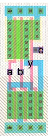
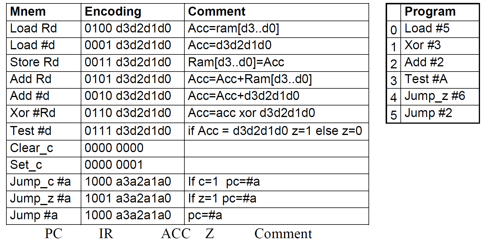
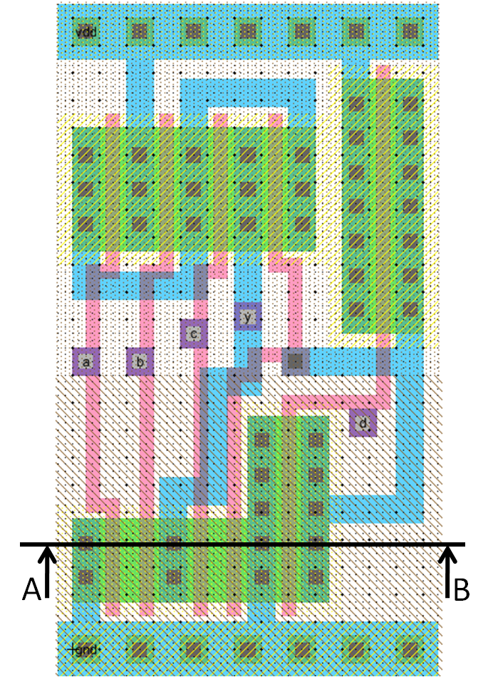
SS 2021 Problem 7: Microprocessor
What are the three states of a instruction decoder of a microprocessor?
What happens during these states? (6 points)
Describe step by step what happens with the registers IR, PC, ACC
and Z during the execution of the program. (12 points)
What simulation is done with this SPICE code? Describe the
circuit, signals and simulation. (5 points)
How many transistors are implemented, what are the dimensions and
what is the transistor model name? (5 point)
What is the operating voltage? (1 point)
Draw v(Vout),V(Vres) versus v(Vin) of this circuit. Label the axis
and important measurement points. Discuss the curve. The PFET has Vtp=-0.8V
and the NFET Vtn=0.8V. IDSN=2*IDSP. (11
points)
SS 2021 Problem 9:
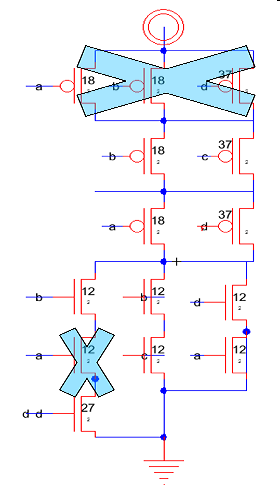
Make a truth table and draw a transistor and a logic schematic for the following logic AOI function. (15 points)
\( Z = \overline{(AB) + (BCD)} \)
A
B
C
D
Z
SS 2022 HKE Examination Microelectronics
SS 2022 1. Problem Manufacturing:
A wafer with 200mm diameter has 1200 Chips.
During manufacturing test 20 chips have contact problems.
40 Chips violate the current limits. 80 Chips are functional fail.
The chips are manufactured in a 90nm technology and need 100F2 per transistor.
What are the contact yield, the DC yield and the total yield? (6 points)
What is the defect density? (2 points)
How many transistors are realized on one chip? (2 points)
What can go wrong during manufacturing of integrated circuits? (6 points)
1.1
\( Y_{contact} = \frac{1180}{1200} = 98.3 % \) (2)
\( Y_{DC} = \frac{1200-20-40}{1200} = 95 % \) (2)
\( Y_{total} = \frac{1200-20-40-80}{1200} = 88.3 % \) (2)
1.2
Defect density = Bad Chips / Wafer area
\( D = \frac{20+40+80}{ \pi \cdot r^{2}} = 0.0045 mm^{-2} \) (2)
1.3
Chip area = Wafer area/Number of chips \( = \frac{\pi r^{2}}{1200} = 26.18mm^{2} \)
(1)
Transistors = Chiparea/100F2= 32320912 = 32Mio (1)
1.4
- Particles too high -> defects: shorts and opens (1)
- Misalignment (1)
-over/underexposure: lateral thick or thin lines (1)
- thickness of deposited layers wrong (1)
- over/under etching/cmp (1)
- wrong recipe (1)
SS 2022 2. Problem Output voltage:
Technology
Scale factor
Rn
Rp
Vthn
Vthp
Cox=Cox·WL(scale)2
50nm
34k Ω L/W
68k Ω L/W
280 mV
-280 mV
62.5 aF·WL
All transistors have a width of 200nm and a length of 100nm.
Give the maximum voltages at the points OUT1, OUT2 and Out for an
operating voltage of 1V. (4 points)
Calculate the delay from In1 to OUT1 through M1. (3 points)
A top view of a metal line in a 90 nm
process running from A to B is shown
crossing a polysilicon line, which runs from
left to right. The metal sheet resistance is
Rsquare = 0.4 Ω / square. The lines are isolated
with 150 nm oxide. (ε0 = 88 fF/cm, εSiO2 = 4)
Calculate the capacitance between
metal line (blue) and the polysilicon
line (yellow).(2 points)
Calculate the resistance from A to B. (2 points)
Draw a cross section from points C to D. (4 points)
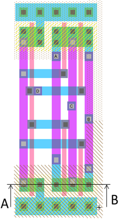
Make a truth table for the following cicuit: (4 points)
D
C
B
A
Y
Draw a transistor schematic with te W/L ratio of the transistors. (6 points)
Give the Boolean equation. (3 points)
Each contact has a resistance of 20 Ω.
What is the minimum and maximum contact resistance of the
source drain contacts of the transistors? (3 points)
Draw a cross section along the line from A to B (5
points)
\( Y = /((A \cdot B) + (C \cdot /D) ) \) (3)
2 contacts in parallel Rmax = 10 Ω
(1)
7 contacts in parallel Rmin = Rcontact / 7 = 2.86 Ω
(2) (5)
Each error -1.
SS 2022 5. Problem: Circuit analysis
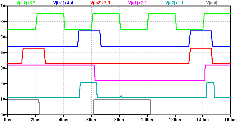
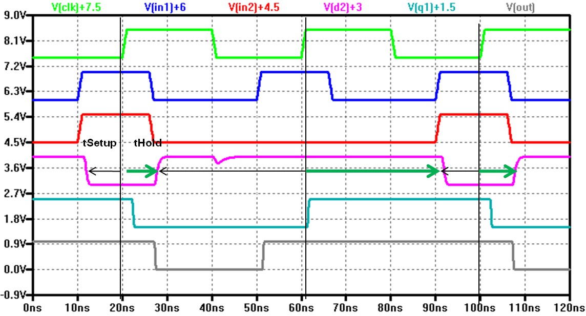
Draw the output response of nodes Q1+2.2, D2+1.1 and Out. (6 points)
What are the setup and hold times? How do you measure a setup and
hold time? (4 points)
Setup Time: 10ns for '1'; 35ns, 75ns, for '0' (1)
Hold Time: 5ns for '1', 30ns, 70ns for '0' (1)
Setup Time: Signal mid level to clock rising mid level (1)
Hold Time: clock rising mid level to Signal mid level. (1)
What simulation is done with this SPICE code? Make a schematic,
describe the circuit, signals and simulation. (5 points)
How many transistors are implemented, what are the dimensions and
what is the transistor model name? (5 point)
What is the operating voltage? (1 point)
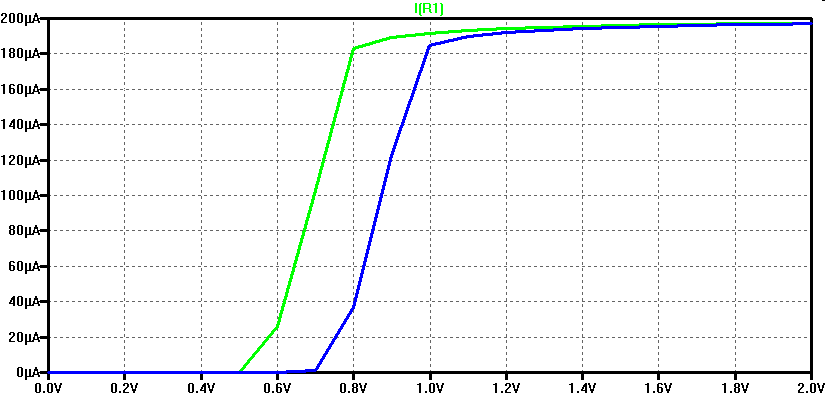
Draw I(R1) versus V(V1) of this circuit for this simulation (Vthn0=0.5V).
Label the axis and important measurement points. Discuss the curve. (5
points)
A DC simulation V1 is varied from 0 to 2 V with 0.1V step. (1)
V3 is varied from 0 to -1V with -1V step. (1)
V2 is constant at 2V.
(3)
2 Transistors are implemented (1)
width=750nm (1)
length 250nm M1 (1)
and 500nm M2 (1),
model name:NMx (1)
3. Operating voltage 2V
x.-axis: V1 gate source voltage
y-axis: drain source current
Transfer characteristic (1)
At V1=0.5V current starts to flow (1)
At high voltages is limited by resistor, linear region. (1)
If well is biased the threshold voltage changes. (1)
Vth will get larger. (1)
SS 2022 7. Problem
How do you cope with complexity? (4 points)
What is a floorplan? (2 points)
What are standard cells? What properties do they have? (4 points)
What is design verification? (2 points)
What is a wired AND fault model? (3 points)
How do you cope with complexity? (4 points)
Hierarchy (1)
Modularity/Reuse (1)
Regularity (1)
Locality (1)
What is a floorplan? (2 points)
A top view of circuit blocks of a chip with an area estimation. (2)
What are standard cells? What properties do they have? (4 points)
Standard cells are logic circuits with a common cell height. (2)
They have a VDD and GND line at the top and bottom (1)
They can be easily placed next to each other and allow easy routing,
since VDD and gnd can be connected easily. (1)
What is design verification? (2 points)
Comparing the actual electric behavior with the specification. (2)
Simulation and measurement of timing and truth table.
What is a wired AND fault model? (3 points)
A fault is modeled as an AND gate. The output is only '1' if both input
signals are '1'. (3)
SS 2022 8. Problem
(1) Make a truth table and draw
(2) a transistor and
(3) a logic schematic for the following AOI function. (15 points)
Z = (ABD) + (BC) + (AD)
A
B
C
D
Z
0
0
0
0
1
0
0
0
1
1
0
0
1
0
1
0
0
1
1
1
0
1
0
0
1
0
1
0
1
1
0
1
1
0
0
0
1
1
1
0
1
0
0
0
1
1
0
0
1
0
1
0
1
0
1
1
0
1
1
0
1
1
0
0
1
1
1
0
1
0
1
1
1
0
0
1
1
1
1
0
SS 2023 HKE Examination Microelectronics
SS 2023 1. Problem Manufacturing:
A wafer with 300mm diameter has 1600 Chips. During manufacturing test 110
chips have contact problems. 80 Chips violate the current limits. 180 Chips are
functional fail. The chips are manufactured in a 60nm technology and need 80F2
per transistor.
1.1 What are the contact yield, the DC yield and the total yield? (6 points)
1.2 What is the defect density? (3 points)
1.3 How many transistors are realized on one chip? (2 points)
1.4 What would be the optimum width to length ratio of a chip? Why?(2 points)
SS 2023 2. Problem Circuit properties:
Technology
Scale factor
Rn
Rp
Vthn
Vthp
Cox=Cox·WL(scale)2
50nm
34k Ω L/W
68k Ω L/W
280 mV
-280 mV
62.5 aF·WL
The circuit is operated with VDD = 1V.
2.1. Calculate the minimum and maximum delay of this circuit.(6 points)
2.2 What is the maximum current of each of the 4 transistors?(5 points)
There is the propagation delay for stage1 t1 and stage 2 t2.
The general equation for the propagation delay time is:
t = 0.7 R C
R is the resitance of the NFET or PFET.
C is the total capacitance at the output.
The maximum current is:
\( I_{maxN0} = \frac{VDD}{R_{N0}} = \frac{1V}{8.5 k\Omega} = 117 \mu A \)
\( I_{maxP0} = \frac{VDD}{R_{P0}} = \frac{1V}{8.5 k\Omega} = 117 \mu A \)
\( I_{maxN1} = \frac{VDD}{R_{N1}} = \frac{1V}{2.125 k\Omega} = 470 \mu A \)
\( I_{maxP1} = \frac{VDD}{R_{P1}} = \frac{1V}{2.125 k\Omega} = 470 \mu A \)
SS 2023 3. Problem Layout and parasitic:
A top view of a metal line in a 50nm process running from A to B is
shown crossing a polysilicon line, which runs from left to right. The
metal sheet resistance is Rsquare=0.6Ω/square.
The lines are isolated with 80nm oxide. (ε0= 88 fF/cm, εSiO2
= 4)
1. Calculate the capacitance between the metal line (blue) and the
polysilicon line (yellow).(2 points)
2. Calculate the resistance from A to B? (2 points)
3. Calculate the voltage drop on the line if a current of 30µA is flowing. (2
points)
4. Draw a cross section from points C to D (4 points)
SS 2023 4. Problem:
Make a truth table for the following circuit: (4 points)
D
A
B
C
Draw a transistor schematic with the W/L ratio of the transistors. (6
points)
Each contact has a resistance of 20Ω. What is the minimum and maximum
contact resistance of the source drain contacts of the transistors? (3
points)
Draw a cross section along the line from A to B (5 points)
SS 2023 5. Problem: Circuit Analysis
5.1 Draw the output response of nodes Q1+2.2, D2+1.1 and Out. (6 points)
5.2 What are the setup and hold times? (6 points)
SS 2023 6. Problem: SPICE netlist
* Testcell
Mnmos0 N001 A 0 0 N L=0.1U W=0.4U
Mpmos0 N001 A Vdd Vdd P L=0.1U W=0.8U
Mnmos1 Y N001 0 0 N L=0.1U W=1.6U
Mpmos1 Y N001 Vdd Vdd P L=0.1U W=3.2U
C1 Y 0 100fF
VD1 vdd 0 DC 1.2
Va a 0 PULSE(0 1.2 5n 1n 1n 4n 10n 20)
.include cmosedu_models.txt
.tran 0 25n 0 0.01n
1. What simulation is done with this SPICE code? Make a schematic, describe
the circuit, signals and simulation. (8 points)
2. How many transistors are implemented, what are the dimensions and what is the
transistor model name? (5 points)
3. What is the operating voltage? (1 point)
4. Draw V(a), V(Y), V(N001) of this circuit for this simulation. Label the axis
and important measurement points. Discuss the curve. (4 points)
SS 2023 7. Problem:
7.1 What is a silicon compiler? (2 points)
7.2 Why do you need DRC? (2 points)
7.3 What is alignment, what kind of alignment problems can happen, how is
alignment done? (4 points)
7.4 What is specified with design rules? (3 points)
7.5 How do you make a robust layout? (3 points)
SS 2023 Problem 8 VHDL:
1. Make a truth or state table for this VHDL code. (8 points)
entity ThisCircuit1 is port (
  clk: in STD_LOGIC;
  a: in STD_LOGIC_VECTOR (1 downto 0);
  b : in STD_LOGIC;
  y: out STD_LOGIC);
end ThisCircuit1;

architecture Behavioral of ThisCircuit1 is
  signal xy:STD_LOGIC;
begin
  PROCESS (clk)
  BEGIN
    if (clk='1' and clk'event) then
      CASE a IS
        WHEN "00" => xy<=xy and b;
        WHEN "01" => xy<=a(0) or b;
        WHEN "10" => xy<=b and xy;
        WHEN "11" => xy<=a(1) and b;
        WHEN OTHERS => xy<='0';
      END CASE;
    end if;
  END PROCESS;
  y <= xy or b;
end Behavioral;
2. Draw a timing diagram of the signals a, b, c, xy and y of this circuit for
the following stimulus. ( 7 points)
   constant Tp : time := 10 ns;
BEGIN
  clk_process :process
  begin
    clk <= '0'; wait for Tp/2;
    clk <= '1'; wait for Tp/2;
  end process;
  stim_proc: process
  begin
    a <= "11"; b <='1'; wait for Tp;
    a <= "10"; b <='0'; wait for 2*Tp;
    a <= "00"; b <='1'; wait for Tp;
    a <= "01"; b <='0'; wait for Tp;
    a <= "11"; b <='0'; wait for Tp;
  end process;;
Questions:
1. What is a suitable unit for area per transistor?
2. Why are you interested in the area per transistor?
3. How can the switch point of an inverter be changed?
4. What is an RCX extraction? Why do you need it?
5. What is a process window investigation? Why do you need it?
6. What rules apply for a standard CMOS cell?
7. When do you do optimization?
8. How many delay times can be measured at a 3 input NOR gate?
9. How many test vectors do you need, if you have a circuit with 3 inputs and 4 registers?
10. A combinational circuit with 8 inputs is tested with 220 test vectors(input signal combinations).
What is your test coverage?


 (5)
(5)