Signal Margin Analysis for DRAM Sense AmplifiersJörg Vollrath, Joerg.vollrath@ieee.orgAbstractThe sense amplifier (SA) design and the bit line architecture determine the minimum detectable signal limit for a dynamic random access memory (DRAM) cell readout operation. Increasing memory sizes, smaller feature sizes and lower operating voltages make it more important to understand the cell signal sensing operation, the signal of memory cells and the limiting factors. This paper presents a measurement method to evaluate the signal created by the memory cell and the sense amplifier uniformity at product level. Measurements of the sense amplifier offset distribution and sense amplifier signals for '0's and '1's for all memory cells will be presented. Spatial analysis gives further insight into the sensing limitations. This can be used to improve the circuit modeling of the sense amplifier and to simulate process variations. The results for a 64Mbit 0.19µm memory device will be shown, having a sense amplifier imbalance. |
Introduction
Dynamic random access memories face the challenge with smaller feature sizes and reduced memory cell capacitance to detect very small signals during a read operation. In a 64M SDRAM device with 8k refresh, 64M/4k=16k sense amplifiers are set at the same time. A sense operation is finished in 5 ns. This requires a lot of charge to set the sense amplifiers. Power wiring and distribution is critical for this operation to get the optimum uniform sense amplifier performance. The layout of the sense amplifier, the robustness to misalignment and variations in dimensions is influencing the sensing operation. A phenomenon where a '1' in a sea of '0's is not sensed correctly is known as the weak column problem in dynamic memories. Therefore it is important to measure the uniformity of the sense amplifier performance on the product with different data patterns and under various operating conditions. Direct measurement of many sense amplifiers is not possible, since the bit lines and sense amplifiers are in a tight pitch on a low metal layer. Some memories have access pads to a couple of sense amplifiers at the border of the memory array. The sense amplifier signal can be measured there using pico probes. The probes can influence the signal. This method is time consuming and gives only a very small number of data points. There are measurement procedures using special test modes on the finished product [1]. The signal measurement can be used to check the circuit simulation and improve circuit models. This paper uses the reduced signal measurement technique [2], generating fail counts and bit fail maps. The analysis of the fail counts and bit fail maps results in an estimate for the cell signal at the sense amplifier.
First the problem will be stated. Then the measurement method will be explained. Measurement results of a 64Mbit DRAM will be shown and discussed.
Problem
A 64M product showed in an early development phase a data topology sensitivity for timing and retention critical memory tests. During the memory test data patterns are written into the cell array. For solid data all memory cells have the same voltage level. A checkerboard data pattern switches between low ('0') and high levels ('1') in adjacent cells [6]. Earlier products had a worst case data topology. This product had memory cells failing exclusively for solid data and other cells exclusively failing checkerboard data. This had an impact on test time, since every pattern had to be run twice with both data topologies. This paper presents the investigation to determine the most critical data topology to optimize the product test strategy and understand the physical root cause for the behavior. The root cause for data topology sensitivities for single cells can be found in the physical memory array structure, for bit lines (BL) it can be found in the BL coupling scheme [3] or the sense amplifier design [2,4].
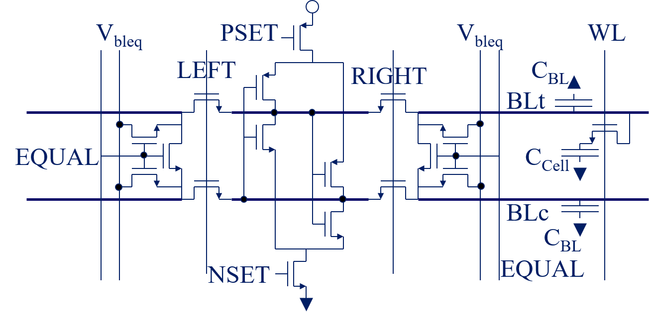
Figure 1: Schematic of a sense amplifier
Figure 1 shows the schematic for a typical dynamic random access memory sense amplifier [5]. The cross coupled inverter arrangement can be seen with the NFET and PFET of the inverters and the NSET and PSET transistors to prevent weak column effects. Since the sense amplifier is shared between left and right bit lines (figure 2) a LEFT and RIGHT isolator is shown. The connection to the Vbleq network to equalize the bit lines, consist of three transistors on the left and three transistors on the right. These are activated by the EQUAL signal. A true (BLt) and a complement (BLc) bit line are connected between the sense amplifier and the memory cell.
The signal equation for the sense amplifier signal assuming constant charge is:
| \( Q_{before}=C_{Cell} \cdot V_{cell} + C_{BL} \cdot V_{bleq} \) | (1) |
| \( Q_{sensing} = \left( C_{BL} + C_{Cell} \right) \left( V_{signal} + V_{bleq} \right) \) | (2) |
| \( V_{signal}= \frac{C_{Cell}}{C_{BL} + C_{Cell} } \left( V_{cell} - V_{bleq} \right) \) | (3) |
VCell: Voltage level in the memory cell
Vbleq: Equalize voltage
CCell: Cell capacitance
CBL: bit line capacitance
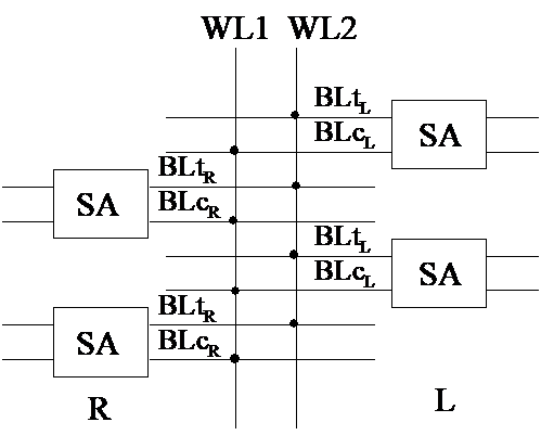
Figure 2: Sense amplifier (SA) scheme
The ideal signal equation has to be extended to include parasitic effects. A neighboring bit line can couple signal via the bit line capacitance CBL. A sense amplifier offset can be caused by a threshold voltage (Vt) mismatch of the sense amplifier NFETs and PFETs. There can be misalignment of the gates, variation in the gate length or mismatch in the series resistance of the drain or source (power wiring). Signal measurements have to be done to model these variations correctly. This investigation uses a special test mode to estimate the signal for a '0' and a '1' with different data topologies and the distribution of the Vt mismatch.
Signal margin measurement set up
The investigation was performed on wafer level, where the internal chip voltages can be controlled via pads. The chip had a test mode to inhibit the sense amplifier setting to use the reduced signal technique [2]. The test flow of the reduced signal test is shown in figure 3. A signal is written into the cell. One or more reduction steps are performed, where the cell is accessed, but the sense amplifier is not set. This stores the signal level on the bit lines back into the cell. Finally the bit line equalize voltage is varied and the cell is accessed. The sense amplifier makes a simple comparison between the bit line equalize voltage and the cell level. If the cell level is higher than the equalize voltage a '1' is read, otherwise a '0' is read. During the test there has to be sufficient time to transfer the Vbleq voltage from the network to the bit lines: 10..100?s. This results in large retention times for the measurement pattern. For a typical device with 8k refresh this results in: 8k * 100µs = 800 ms retention time. A special test pattern using only sub blocks of the whole memory array can reduce the retention time.
As a result fail counts are measured versus the bit line voltage Vbleq level. Since a large number of cells, bit lines and sense amplifiers are involved the variations of the signal will be Gaussian distributed. Therefore a normal probability plot of the failcount is done. The failcount is normalized to the percentage of total tested memory cells.
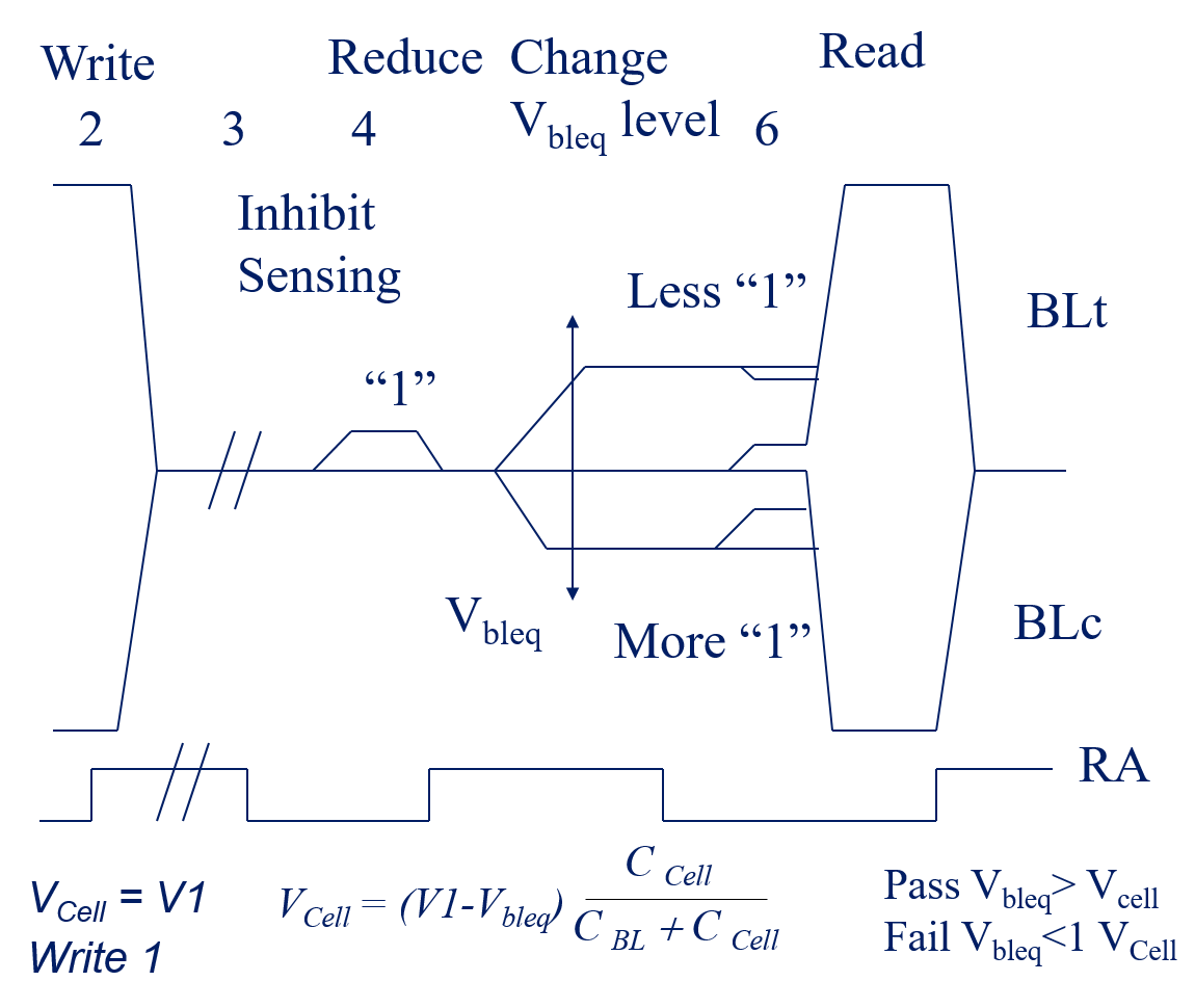
Figure 3: Reduced signal test flow
The following section presents the results.
Results
All measurements were done at room temperature on 8Mbit of cells of a 64Mbit DRAM. For some measurements the memory cells were divided into four groups: true and complement bit lines and left and right sense amplifiers. The device operated with a memory cell array voltage of Vblh =1.8V, a bit line equalize voltage Vbleq = 0.9V, an internal regulated voltage Vint=2.3V for the periphery and a wordline voltage of Vwl=3.3V.
No reduction
To get a base line for the sense amplifier circuit the first test writes the level '0' or '1' in the cell, uses no reduction step and simply varies the Vbleq during the read operation and measures the fail count. Figure 4 shows the result. The x axis shows the Vbleq variation and the y axis the normalized cumulative percentage of the fail count.
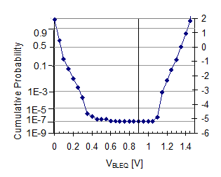
Figure 4: Probability plot: fail count percentage versus Vbleq voltage with no reduction step.
The vertical line at 0.9V in figure 4 shows the level of the nominal Vbleq. Above Vbleq(reduction=0,'1') = 1.1 V the sensing operation of the '1' is limited. The fail count increases. Below Vbleq(reduction=0,'0') = 0.3V the sensing operation of the '0' is limited. This is an asymmetry in the measurement scheme. The level for the '1' can only be limited by the word line voltage Vwl=3.3V or by the LEFT and RIGHT isolator transistors, which are operated with Vint =2.3V. It was confirmed by increasing Vint and keeping Vwl constant, that the transferred signal is limited by the threshold voltage of the LEFT and RIGHT isolator transistors.
Reduction and solid data
Measuring the fail count for one reduction for solid '0' data and solid and checkerboard data for '1's gives figure 5. The cross point of the '0' and '1' curve gives the mid level voltage: Vmid=0.92V. This can be caused by word line voltage coupling during activation to the bit lines [2]. The signal for the '0' at 50% fail count is Vbleq (reduction=1,'0') = 0.92V-0.72V = 200 mV. For the '1' at 50% fail count the signal is Vbleq(reduction=1,'1') = 1.1V-0.92V = 180 mV. The signal is barely below the limit of the operation range of 1.1V. Further measurements bumped the Vbleq and the cell voltage by a factor of 1.5 during read. A difference can be seen for solid and checkerboard data. This is expected since the product data already showed data topology dependencies. A spatial analysis was done to confirm that.
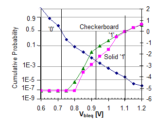
Figure 5: Probability plot fail percentage versus Vbleq voltage with one reduction step.
Bit fail map spatial analysis
Bit fail maps were taken for solid '1's between 1.25 and 1.60 V Vbleq. The voltages including the cell voltage were bumped up 1.5 times during Vbleq variation to ensure that there was no signal limit from the LEFT and RIGHT isolator transistors. Figure 6 shows the probability plot and figure 7 the bit fail maps. The curves are shifted to higher voltages as expected. This measurement was done on a different chip. A slight change in the '1' signal can be observed: V('1')= 1.51-1.35V = 160 mV. This is probably due to the bump of the voltage. The cell signal is not fully bumped up to the higher voltage. The Vbleq step size was 10mV compared to the 50mV step size before. This leads to the two nice lines with an unexpected step at 1.375V.
For every test step a full bit fail map was saved and a screenshot of a bit fail map tool was taken. 35 bit fail maps 64Mbit each take a total of 2 Gbit of memory. The bit fail maps were processed for pass/fail transitions of each individual cell. The fail count curve shows that a 10mV resolution is necessary to get accurate transition results and that the range from 1.25 V to 1.6V is sufficient to capture the lower part of the signal distribution, but not for the higher part. The amount of chips, which can be characterized is limited by the long test time, storage space and processing time to fully analyze the bit fail maps spatially.
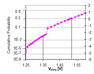
Figure 6: Fail count measurements for the bit fail maps
The 8 bit fail maps in figure 7 are twofold. On the left side is an overview of the chip. It can be seen that only a 1/8th of the chip is tested. On the right side for each map is a zoom picture. The bit lines are vertical in the picture. It can be seen that complete bit lines are failing with a variation of Vbleq. This shows that the transition is not caused by weak cells, but by bit line coupling, limiting isolator device or sense amplifier mismatch. The overview of the whole chip shows the weakest bit lines. The zoomed in bit map visualizes the median of the distribution. It is interesting to observe, that a true or complement bit line transition from pass to fail occurs in a 10mV step. Either the cells along one bit line must have a very uniform signal distribution, or the signal for the sense amplifier is limited by the isolator device.
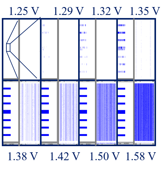
Figure 7: Bit fail maps for the '1' with Vbleq variation
A spatial analysis looked at the transition voltage from pass to fail of true and complement bit lines of the right and left sense amplifiers. Figure 8 shows the number of the sense amplifier on the x-axis and the Vbleq transition voltage on the y-axis. This shows a huge spread in the transition voltage in a small area. A systematic offset of 50-80 mV between true and complement bit lines (LL,LR) can be seen (Figure 9). For some bit lines no transition from pass to fail can be observed, since the maximum limit of the Vbleq was 1.6V. Only 80% of the cells were failing at 1.6V. Further investigation with the layout has to be made to determine the root cause of these points.
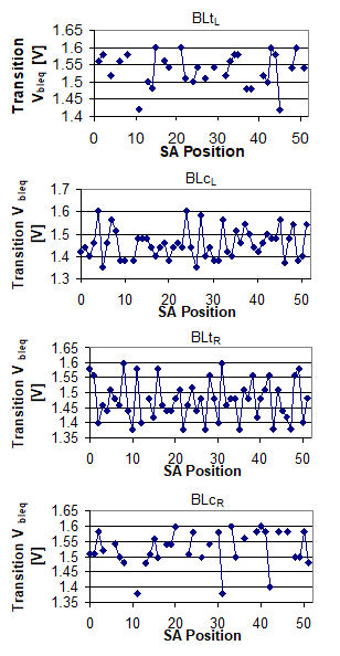
Figure 8: Transition of the bit lines for the left (BLL) and right (BLR) sense amplifiers and true (BLt) and complement (BLc) bit lines
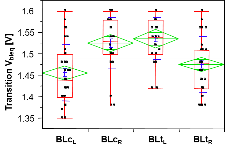
Figure 9: Sense amplifier distribution
Conclusion
This paper showed the importance of signal margin analysis for high density DRAMs. A systematic sense amplifier offset for a 64Mbit product in the development stage could be shown. This method is a useful tool to compare the sensitivity and mismatches of different sense amplifier layouts. The measurement method is simple, requiring only one test mode and access to the internal Vbleq voltage.
The measurement is very time consuming due to the pattern run time. It needs specialized bit fail map analysis tools to generate the transition points. Spatial analysis can detect systematic pattern in the transition caused by sense amplifier mismatches. This method can compare different sense amplifier layouts in an actual product. This can result in improving a sense amplifier design. This method will become more useful for future memory products with higher number of memory cells and more process variations due to the smaller feature size.
References
[1] Kirihata, T., Hing Wong, DeBrosse, J.K., Watanabe, Y.; Hara, T., Yoshida, M., Wordeman, M.R., Fujii, S., Asao, Y., Krsnik, B., Flexible test mode approach for 256-Mb DRAM , IEEE Journal of Solid-State Circuits, JSSC, Volume: 32 Issue: 10 , Oct. 1997,pp. 1525 -1534
[2] Joerg Vollrath, Cell measurement for high density DRAMs, International Test Conference, ITC, Washington DC, 1997, pp 209-216
[3] Dong-Sun Min; Langer, D.W., Multiple twisted dataline techniques for multigigabit DRAMs, IEEE Journal of Solid-State Circuits, JSSC, Volume: 34 Issue: 6 , June 1999, Page(s): 856 -865
[4] Geib H., Weber W., Wohlrab E., Risch L., Experimental Investigation of the Minimum Signal for Reliable Operation of DRAM Sense amplifiers, IEEE Journal of Solid-State Circuits, Volume: 27 Issue: 7 , Jul. 1992,pp. 1028 -1036
[5] T. Kono, T. Hamamoto, et. Al, A Precharged-Capacitor-Assisted Sensing (PCAS) Scheme with Novel Level Controllers for Low-Power DRAM's, IEEE Journal of Solid-State Circuits, Volume: 35 Issue: 8 , Aug. 2000,pp. 1179 -1186
[6] Joerg Vollrath, Tutorial: Memory Test Construction: A Field Approach, IEEE Proceedings of the Memory Technology, Design and Test Workshop (MTDT), San Jose, 2000, pp. 59-64