Test and Characterization of SDRAMsJörg Vollrath, Joerg.vollrath@ieee.orgAbstractTo improve yield and product quality, SDRAM manufacturers perform a variety of tests. A test sequence that incorporates retention tests, signal margin tests, and speed tests can help manufacturers find and repair weak memory cells. |
This article describes, from a manufacturing perspective, memory cell array testing using signal margin tests, and retention tests using simple patterns. It demonstrates that these tests are as important as functionality and speed tests and that the pattern is only one variable of the test strategy.
Using more than one test requires a test sequence and detailed data generation for diagnosis. Having the right test sequence with optimal data collection means shorter test times and shorter product learning and improvement cycles, facilitating failure diagnosis and thus improving device manufacturability. In this article, I hope to simplify fault coverage evaluation for memory devices and to assess the abilities of BIST for embedded memory products.
Manufacturing test flows
Figure 1 shows a typical SDRAM test flow with five electrical test gates. The prefuse test reads and writes all cells at the wafer level and tries to construct a redundancy solution to replace bad memory cells with spare cells. This information then goes into the fuse banks electrically or by laser. A postfuse test verifies the fuse success. During assembly, wafers are diced and the resulting chips are packaged. Burn-in involves exercising the components for some time at high temperatures under high-voltage conditions. This catches early failures and improves chip quality. The manufacturer then tests the chip's functionality at low and high temperatures according to the device specification.
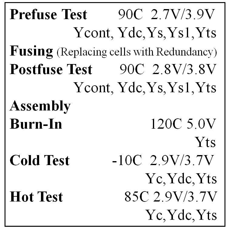
Figure 1. A typical SDRAM manufacturing test flow showing the test and assembly stages and yield definitions.
High yields are important for successful manufacturing. Yields are the number of good chips divided by the total number of chips tested. Figure 1 shows the yields used in typical manufacturing test flows:
- Contact yield (Ycont) looks for gross chip failures, missing pads, and shorts or opens directly at the inputs. It also measures the condition of the test equipment. Poor contact at the needles or dirt in the fixtures can affect contact yield.
- Dc yield (Ydc) measures the current at different operating conditions.
- Screen yield (Ys) measures a chip's basic functionality such that every memory cell passes a basic read-write test (a screen test), or, if they fail (a hard fail), such that they are repairable. In SDRAM memory processes, redundant memory cells replace defect cells.
- Perfect yield (Ys1) is the number of chips that have no hard failures divided by the total number of chips.
- Test sequence yield (Yts) can be the absolute yield compared to the total number of chips on the wafer or the relative yield compared to the number of screen-tested good chips.
SDRAM functionality
To properly characterize SDRAMs, test engineers must understand an SDRAM's internal circuits and their operational functions. An SDRAM data sheet shows a block diagram of the internal circuits. A designer can configure an SDRAM for column access strobe (CAS) latency and burst length. CAS latency (CL) is the time between applying an external address and getting data from the chip. A burst length determines the amount of data transferred in consecutive cycles between the memory controller and the memory after applying one start address. During an access, the memory chip selects a memory location using a row address (x) and a column address (y). The memory activates one of four banks according to the bank address. The memory transfers the information between the memory cell and the input and output buffers through the data path. Input and output buffers connect the data to the external pins.
For every row address, a timing circuit in the memory selects a word line (WL), reads out all cells along the WL to sense amplifiers, and refreshes the cells with a write back. A column select connects one sense amplifier to the data path. A read transfers information to the external pads, and a write transfers data from the external pads to the sense amplifiers. A write can also flip the sense amplifier to the opposite data so that 0s become 1s, and vice versa.
SDRAM commands, addresses, and data are latched to the rising edge of a clock (CLK). Basic SDRAM operation consists of an activate (ACT), read (RD), or write (WR) command followed by a precharge. An SDRAM uses additional commands (such as NOP (no operation) or DESL (deselect)) as time fillers. A refresh command (REFR) refreshes all cells for one row address in all banks.
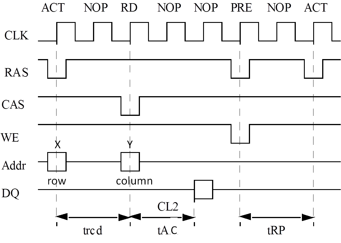
Figure 2. Timing diagram of an SDRAM access. For the access, the CAS latency is 2 because data is available at the outputs two cycles after the read command.
The CAS latency is 2 because data is available at the outputs two cycles after the read command. When the memory controller programs a burst length of 1, the memory supplies one data bit. The latency provides enough time for the internal circuits to select a column address and deliver valid data to the outputs. Important timing parameters for internal operation included the following:
- tRCD (typically 15 ns) is the time between the activate command and the first read or write command. Internally, a decoder circuit must decode a WL and read out the cell to the sense amplifier before a column select can connect the sense amplifier to the data lines.
- tAA (typically 15 ns) is the time needed to select a column and transport data from the sense amplifier to the output pads.
- tWW (typically 6 ns) is the time needed to transport data over the data lines from the inputs to the sense amplifiers, which are decoded with the correct column address, and over the bit lines into the memory cell.
- tRP (typically 15 ns) is the time it takes for the equalize circuit to disconnect the cell from the sense amplifiers and the sense amplifiers to equalize in preparation for the next access.
Basic screen test
A basic screen test involves applying a voltage level to a chip and then specifying a pattern, which determines the operation sequence, and a timing set. Van de Goor has implemented a notation for specifying a test pattern and a failure type.[1]A march test is a simple basic screen test. A typical march test tests all cells in a memory array by writing data to the whole array and then reading the data. Next it writes and reads opposite data for the entire memory array. A normal data write concludes the pattern. A march test ensures that the addressing works and that all cells can store and retrieve "0" and "1" information. Because this test performs five operations on all N memory cells, it is a march 5N, and can be expressed as {⇑(r0); ⇑(r0, w1); ⇑(r1, w0)}. This scientific notation describes only part of the pattern. It does not include the initialization sequence, voltage and timing information, or start and step size values for the counting.
Figure 3 gives a graphical representation of the march 5N sequence. The test covers stuck-at faults and addressing faults.
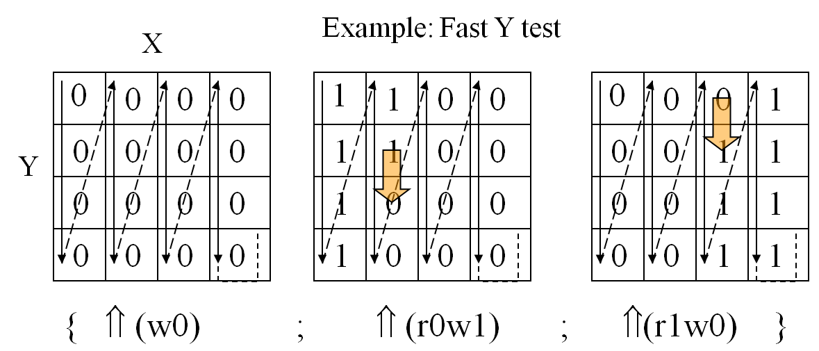
Figure 3. A fast y march test.
A typical march test has five operations: It tests all cells in a memory array by writing data to the array and reading that data, then writes and reads opposite data for the entire memory array, and concludes with a normal data write.
I split each element of the march test sequence into smaller parts. ⇑ denotes a sequence traversing the array incrementing the address. The sequence must specify whether to increment the x or the y address first. Neither the step size nor the addressing sequence is specified. The step size can be any odd number (1, 3, or 5 in a march 5N test) to address all memory cells in one run. Additionally, a scrambler-a transformation of an address-can modify the sequence.
The w0 term denotes a write operation of 0s. For an SDRAM to accomplish this operation, it needs two commands. A typical write sequence is (w): ACT(x), NOP, WD (data) (y), PRE, NOP. Every command (ACT, RD, WR, and PRE) needs an associated timing set. A timing set has a cycle time and times for the rising and falling edges for all control signals (row access strobe (RAS), CAS, write enable (WE), and so on).
For a 100-MHz/133-MHz device, the cycle time (tCYC) is typically (10 ns)/(7.5 ns). I calculate the pattern's runtime using the following equation, which incorporates the burst length (BL) and the cycle time (tCYC):
tRUN = tCYC x{[1 + (y/BL)(6 + BL)] + 2(1 + (y/BL)(6 + 2BL)]}
Preparing for a column access uses six cycles per burst, and selecting a row address takes one extra cycle. The parts of the equation in brackets describe one write step and two read-write steps.
Runtime and pattern retention
Tables 1 and 2 give times for a 256-Mbyte device organized as 16 kbits x, 512y, 8 DQs and 16 kbits x, 1 kbit y,4 DQs, with a 10-ns cycle time and different burst lengths, where DQ represents the number of input/output pads. The tables show an increase in runtime for a times-4 organization over a times-8 organization.Table1. Runtime and intrinsic pattern retention time of a march 5N test for a 256-Mbyte DRAM organized as 16 kbits ??512 ??8, with tCYC = 10 ns.
| Parameter | Burst length | |||
| 1 | 2 | 4 | 8 | |
| Runtime (s) | 1.93 | 1.17 | 0.80 | 0.61 |
| Pattern retention time, fast y (ms) | 671 | 420 | 294 | 231 |
| Pattern retention time, fast x (ms) | 1.47 | 1.80 | 2.46 | 3.77 |
| Parameter | Burst length | |||
| 1 | 2 | 4 | 8 | |
| Runtime (s) | 3.86 | 2.35 | 1.59 | 1.22 |
| Pattern retention time, fast y (ms) | 1342 | 839 | 587 | 462 |
| Pattern retention time, fast x (ms) | 1.47 | 1.80 | 2.46 | 3.77 |
tRET = tCYC x{1 + (y/BL)(6 + 2(BL))].
For a fast y test, the retention time is longer than the 64 ms specified in the data sheet. When the pattern-retention time is greater than the data sheet value, the tester must insert extra refresh cycles, using one x address at a time for the whole array, into the pattern. The retention time for accessing the same WL in a fast x pattern, in which the x and y counting switch between the outer and inner loops, is
tRET = tCYCx{1 + (6 + 2BL)].
The numbers in Table 1 are well below the specified retention time for fast x patterns, which is why I typically use these patterns for testing SDRAMs.
To reduce runtime and intrinsic retention time, I use a bank-interleaved operation. An SDRAM normally has four banks (A, B, C, and D), which can operate independently. I replace the NOP commands with commands for the other banks. A typical read-write operation in which CL = 2 and BL = 4 would appear as
(Read) ACTA; NOP; PREB; RDA; ACTB; NOP; PREC; RDB; ACTC; NOP; PRED; RDC; ACTD; NOP; PREA; RDD; (Fill to prevent data collision) NOP; NOP; (Write) ACTA; NOP; PREB; WRA; ACTB; NOP; PREC; WRB; ACTC; NOP; PRED; WRC; ACTD; NOP; PREA; WRD; (End) PRE
This pattern always produces seamless data and reduces pattern runtime. Comparing runtimes for the read-write operation gives a normal access of
tRUN = tCYCx[1 + y/BL(6 + 2BL)] = 293 ms
and an interleaved access of
tRUN = tCYC(x/4)34y/BL = 178 ms
Activating four banks simultaneously also reduces the intrinsic retention time by a factor of 1.7. In 15 cycles, one WL is activated, whereas 34 cycles require four activated WLs: 15/(34/4) = 1.7.
After examining the bit failure map results, I modify the basic pattern to test for the data sheet specifications. To modify retention tests and signal margin tests, I insert a disturb section between the write and read operations: {⇑(w0); ⇑(d); ⇑(r0w1); ⇑(d); ⇑(r1w0)}. Speed testing applies a critical timing set to a pattern or modifies the pattern sequence. For example, say tRCD is the time between an ACT and a RD or WR command. I can change this using a certain clock cycle time for a command or by inserting or deleting NOP commands in the sequence between ACT and NOP.
Failure data
A catch ram, which physically represents the memory, or a fail vector memory can store march test failures. Figure 4 shows different failure categories for a typical chip bitmap from a catch ram: column select (CSL), WL, BL, and single cell (SC) failures. A failure count can be calculated from a full or compressed bit failure map, and failure types can be distinguished by their appearance on the bit map.4
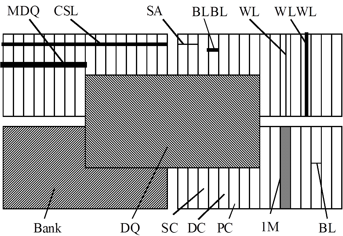
Figure 4. Failure signatures in a typical chip bitmap from a catch ram.
Every black dot represents a failing memory cell. Each dot's position relates to the physical position of the defect on the memory chip.
Failures can be associated with certain process levels[5]. Bit line bit line (BLBL) shorts, for example, indicate a metal process. If bitmaps are available, it is easy to generate wafer and lot maps. Wafer maps can point out certain problem areas, such as the wafer's center or edge. Lot maps can show chamber dependencies if every second wafer shows a different picture and was processed in a two-chamber system. These maps are more valuable than simple pass/fail information because a designer can extract detailed information about the failure's root cause.
Modified march test for manufacturing
I modified a simple march test for signal margin tests, retention tests, speed tests, and functionality tests as used in a manufacturing environment. A real memory test adds timing and voltage conditions to the simple march test pattern. Additional commands in the pattern can also change the timing conditions, such as the retention time.Retention tests
An applied retention time consists of the intrinsic pattern retention time and can be reduced by adding refresh cycles in the pattern. For dynamic memory, only one data type has a critical retention time because leakage currents bring the memory cell to a defined level after a long wait time.A retention time used while the device is active, as in a fast y march test, is the active retention time. A passive retention test uses a pause-a few milliseconds during which the device sits idle-between write and read. Passive retention tests typically use a fast x pattern. The test can either suspend the clock and use an external timer to determine the pause or perform a NOP loop for the desired retention time. As Tables 1 and 2 show, the test can add retention time to the pause using the pattern's w0 and r0w1 operations to access the same WL.
Accesses to adjacent cells can couple directly to either the tested memory cell or the access transistor. Because this coupling can be static or dynamic, I use long parallel select tests (LPSTs) and short parallel select tests (SPSTs), which Figure 5 shows. The test accesses the neighboring memory cell or toggles the neighboring WL for the full retention time. Doing so for all cells requires an xtRET pattern runtime, which is 4 kbits x 64 ms = 256 seconds - quite huge compared to the simple march test. Kirihata and colleagues use a test mode in which more than one WL is accessed at one time [2].
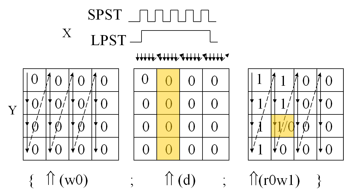
Figure 5. Long parallel select tests (LPSTs) and short parallel select tests (SPSTs) disturb retention patterns.
The characterization curve in Figure 6 measures failure counts against retention time.
I generated these curves at nominal temperature (NT), low temperature (LT), high temperature (HT), and high voltage (HV). A medium retention time (in which half of all memory cells are failing) can range from 5 to 10 seconds at 70°C to 80°C - quite a huge time guardband compared to the 64-ms data sheet specification. An examination of the first failure and its repairability, up to approximately 100 failures, shows a range of 100 ms to 500 ms, which more closely corresponds to the data sheet. The main distribution of retention time is above 500 ms, representing intrinsic retention time, and a tail below 500 ms represents extrinsic retention time.
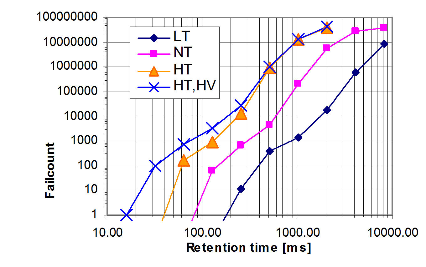
Figure 6. Temperature- and voltage-dependent retention failure count.
The number of failing cells increases at higher retention times and higher temperatures.
Signal margin test
A signal margin test changes the voltage for storing information in the cell or reading information from the cell. Figure 7 shows a cell's write, reduction, and read operations [6]. The scheme's parameters are the cell's voltage level for a 1 and a 0 and the bit-line level during Vbleq sensing. The signal equation for a DRAM memory cell attached to a bit line seen by the sense amplifier isVSignal = (VCell - Vbleq) CCell/(CCell + CBL)
where Vbleq (equalized bit line voltage) is 1.0 V, VCell (cell voltage level) is 2.0 V, CCell (cell capacitance) is 40 ff, CBL (bit line capacitance) is 200 ff, and VSignal (sense amplifier signal) is approximately 170 mV.
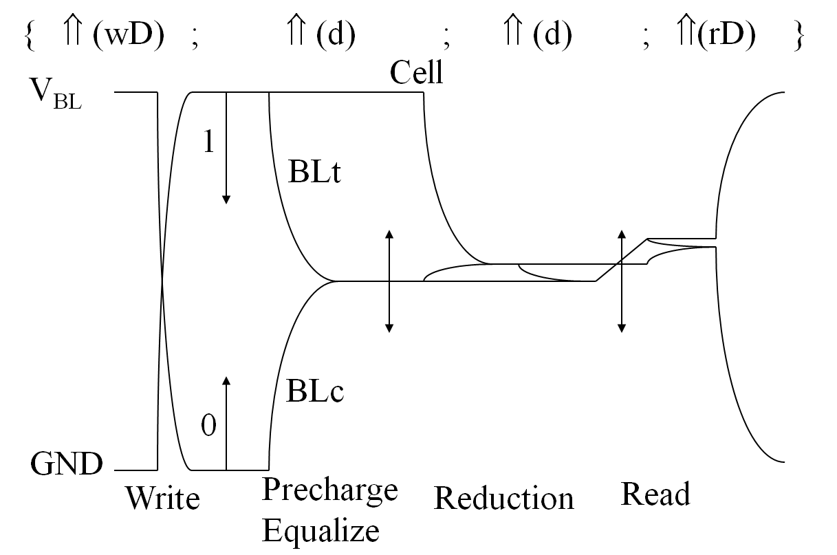
Figure 7. A signal margin test of a cell's write, reduction, and read operations.
The diagram shows the operation sequence and the voltage levels on the bit line.
Typical values for a DRAM technology result in a signal of approximately 100mV to 200mV. The equation shows the effect of limiting the maximum cell signal VCell or changing the Vbleq level during a read operation.
Varying the cell signal during the write, or on the bit line during the read, gives a smaller differential signal on the bit lines. Coupling from neighboring cells and sense amplifier mismatch will result in small signal levels and finally give a read fault. The test will detect weak cells with low storage capacitance or bad connections to the sense amplifier. For characterization purposes, a reduction step can separate the write and read operations [6].
A voltage bump test is another signal margin test approach. The power supply voltage changes between the write and read operations. Typically, the test writes a small signal into the cell and then reads it out with high voltage conditions.
Speed tests and Shmoos
Speed testing verifies SDRAM performance according to its specifications. SDRAMs operate at frequencies of up to 133 MHz. Conventional memory testers operate at 25 MHz to 75 MHz. To achieve higher frequencies, more than one pattern generator operates in parallel-for example, parallel and multiplexed testers use two, four, or eight generators. Because higher frequencies result in line noise, characterization normally uses slower test systems. To test for timing parameters, I drop fill cycles and use asynchronous timings instead.I drop NOP cycles between ACT, RD, PRE, and ACT from the normal sequence shown in Figure 2. Some cycles are needed to support the CAS latency of 2. The clock signal in the ACT cycle comes late and the CLK signal in the RD cycle comes early. The minimum CLK rise and fall times and the cycle length both limit timing variations. Baker [7] explains the Shmoo technique of looking for pass or fail information and varying one or two parameters. Vcc often serves as the second variable.
Figure 8 shows a resulting Shmoo plot for a 64-Mbyte SDRAM.
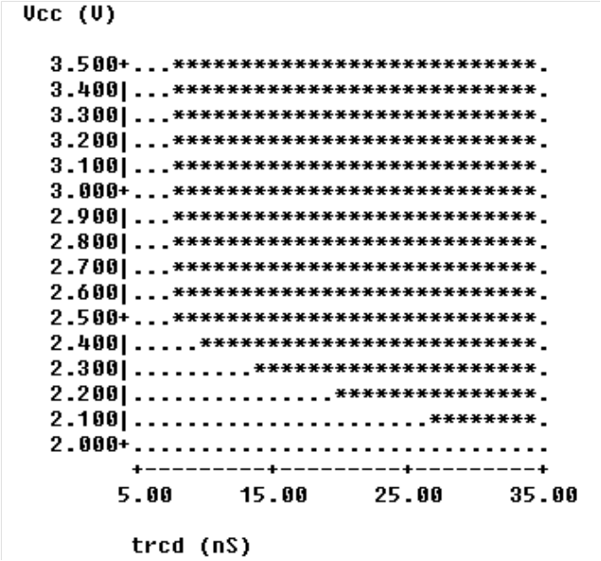
Figure 8. Shmoo plot of tRCD and Vcc. In the diagram, "*"denotes a fail, and "-" denotes a pass.
At every Shmoo point the tester applies a certain timing and voltage condition and test pattern to the memory device. The "*" region denotes a test fail, and "-" denotes a test pass. The transition from "*" to "-" is called pass fail border. The Shmoo in Figure 9 indicates that circuits regulate the device's voltage internally. Above a certain voltage, tRCD is fixed. At lower voltages, transistors switch more slowly, and tRCD increases. A Shmoo with simple pass/fail information can be extended to show a failure count. At the pass/fail border, the tester can generate a bit failure chip map. Figure 9 clearly shows the chip's internal signal distribution for tRP.
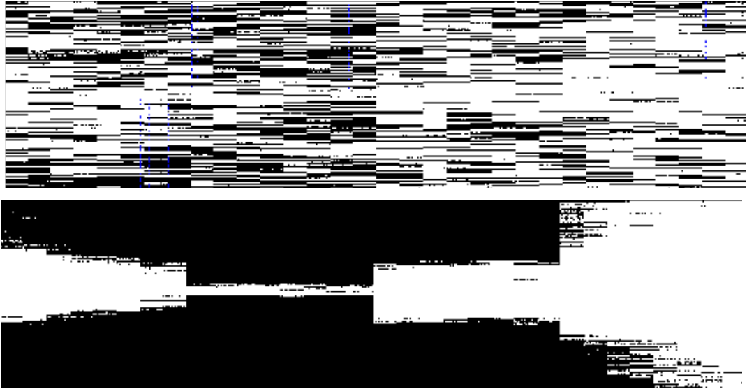
Figure 9. Bit-failure map for a minimum tRCD and tRP.
The black dots show the failing memory cells at the corresponding physical positions on the memory chip.
Areas farthest away from the signal source fail first. This method can help a designer find a chip's most time-critical path.
Functional tests
Many modern SDRAM operational modes exist. Memory controllers can use CAS latency, burst length, and sequential or interleaved data. To do so, they must first check the logic functionality of these modes. The memory is written in one mode for example, CL = 2, BL = 4 sequential) and then read in another mode (CL = 3, BL = 8 interleaved, for example). To cover all failure types, you must perform all these tests with critical timings and the right data topology.Test sequence generation
A good test flow is optimized for all requirements. When selecting a test sequence, a designer must consider fault coverage, diagnosis, and manufacturability. Fault coverage and diagnosis require many lengthy tests and extensive data collection. Manufacturability requires high throughput and only limited fail categories. Table 3 lists typical test sequences and their motivations.Table 3. Test sequences and their motivations.
| Test sequence | Motivation |
| Check equipment and handling | VF: Contact check diode current voltage characteristic (forward voltage) |
| Look for power supply current failures caused by defects or degradation | Active and standby current |
| Check for correct reading and writing of every memory cell | Basic screen test |
| Test functionality with minimum timing requirements | Burst length, CAS latency, and sequential and interleaved operation |
| Check timing requirements | Internal timing tests, tAA, tRP, tRCD, and tWW |
| Measure cell signal | Signal margin test, retention test (active, passive, or data topology), LPST, SPST, or combined test (signal margin and retention, for example) |
| Perform speed sorting | Speed tests using critical setup, hold times, and levels |
Component tests can hardly influence a chip's internal voltages, because most memory designs have internally regulated voltages. High parallelism during test means that the test equipment generates no bit fail maps, but only pass/fail information for every test. A test sequence of test number 00, 03, 41, 42, 43, 51, 52, 53, 61, 62, 63, 64, 65 generates the following information:
Chip1:...F.........
Chip2: .........F..
Every line has pass (.) or failure (F) information for each chip, for every test in the sequence. With highly parallel testing, a failing device doesn't stop the test sequence, because enough passing devices remain in one test touchdown. A designer can extract a failure signature by looking at a device's failed tests, which helps to characterize and diagnose the failure. A full failure string also prepares for test time reduction because a designer can analyze test interaction.
Figure 10 shows a typical test correlation table.
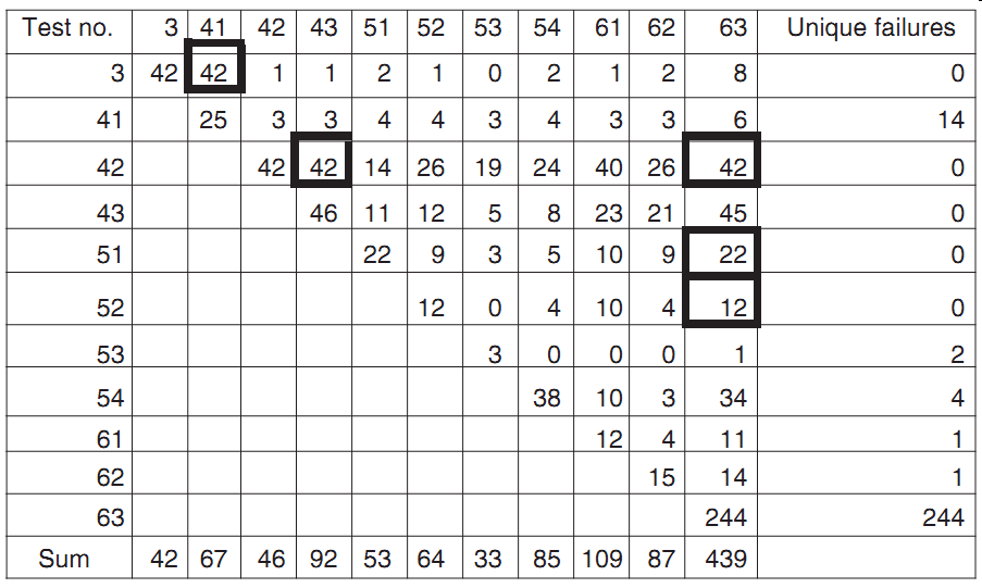
Figure 10: Test sequence evaluation.
The numbers on the diagonal are the failures for a given test sequence; numbers on the bottom line refer to the parts failing a certain test; and the numbers above the diagonal are the correlations between tests. You can identify strong tests by finding a lot of failures, such as tests 63, 61, 43, and 54. Some tests have unique failures-for example, test 53 has 33 total and two unique failures. Weak tests, which find no unique failures for a large number of parts, are marked with a solid border in Figure 10, and can be eliminated, thus improving throughput. Test sequence optimization for diagnosis and throughput is an important part of test engineering.
Conclusion
Future memories will be larger-for example, 512 Mbyte, 1 Gbyte, 2 Gbit and so on - which will require more test time and will complicate bitfailmap analysis. Higher parallelity, shorter test times, or BIST can resolve these problems. The tests and test results presented in this article can serve as a guideline for implementing BIST and parallel test. Higher paralellity or BIST complicates data collection and analysis. Diagnosing weak cells using the presented test data and optimized tests can reduce the number of memory tests as well as test times. New memory interfaces such as DDR-I and DDR-2 will also change testing approaches and pose new challenges for testing strategy.References
1. A. Van de Goor, Testing Semiconductor Memories, John Wiley & Sons, New York, 1991.2. T. Kirihata et al., "Flexible Test Mode Approach for 256-Mb DRAM," IEEE J. Solid State Circuits, vol. 32, no. 10, Oct. 1997, pp. 1525-1533.
3. A. Van de Goor, "Industrial Evaluation of DRAM SIMM Tests," Proc. Int'l Test Conf. (ITC 00), IEEE Press, Piscataway, N.J., 2000, pp. 426-435.
4. M. Sugimoto and T. Hamada, "Application of a Bitmap Analysis System to the Forefront of DRAM Devices Development," Proc. IEEE/SIMI Advanced Semiconductor Manufacturing Conf. (ASMC), IEEE Press, Piscataway, N.J., 1997, pp. 222-227.
5. A. Chan et al., "Electrical Failure Analysis in High Density DRAMs," Proc. IEEE Int'l Workshop Memory Technology, Design, and Testing (MTDT 94), IEEE CS Press, Los Alamitos, Calif., 1994, pp. 26-31.
6. J. Vollrath, "Cell Signal Measurement for High Density DRAMs," Proc. Int'l Test Conf. (ITC 97), IEEE Press, Piscataway, N.J., 1997, pp. 209-216.
7. K. Baker and J.V. Beers, "Shmoo Plotting: The Black Art of IC Testing," IEEE Design & Test of Computers, July-Sept., 1997, vol. 14, no. 3, pp. 90-97.