Implementation and Testing of a FPGA Based Sigma Delta Analog to Digital ConverterMartin Knauer, Jörg Vollrath, University of Applied Science Kempten, Germany, Joerg.vollrath@hs-kempten.deAbstractIn this work a 10-bit sigma-delta analog to digital converter was implemented using only a NEXYS 3 FPGA board in combination with some passive components. In addition, a simple R2R digital to analog converter was implemented, which allowed testing the ADC with synchronous digital signals produced by the FPGA. INL and DNL was measured for both devices. The overall setup revealed a SNR of 33.8 dB with an ENOB of 5.3 bits. But with some minor adaptations (e.g. compensa- tion of an offset error) a resolution of up to 8 bits can be achieved. It was shown that with such a simple approach a fully functioning sigma-delta analog to digital converter can be built. Index Terms-Sigma-Delta Converter, R2R DAC, FPGA. |
I. Introduction
Sigma-delta (Σ-Δ) analog to digital converters are very popular in industry. They provide high resolution for low-price production costs [1]. Furthermore, the basic structure is relatively simple and can easily be implemented in nano-CMOS processes [2]. This makes sigma-delta ADCs ideal for applications such as industrial sensing, audio, and narrow bandwidth radio frequency devices. In this work, a real sigma-delta ADC was realized with a NEXYS 3 FPGA board (Digilent) and some passive components. Furthermore, the FPGA board in combination with a self-made 10 Bit R2R DAC was used to generate clock-synchronous analog signals to test and observe the limits of the DAC. The goal was to test and verify the implemented ADC and show possibilities and limits of such an approach by only using relatively simple hardware.
II. The Sigma-Delta Topology
The main principle of an ordinary 1st-order Σ-Δ converter is based on oversampling, where the internal sampling rate is much higher than the maximum frequency of the analog input signal. The oversampling rate (OSR) is thereby defined as the quotient of the internal clock rate and the input bandwidth.
The input voltage is summed with the output of a feedback loop first and is then connected to an integrator. A comparator outputs a logic 1 if the integrator output is greater than, or equal to zero volts and otherwise it outputs a logic 0. By using a 1-Bit DAC, the digital output is then fed back to the summing node and subtracted from the input signal. This is repeated according to the OSR, which increases the accuracy of the converted signal [2]. The resulting Bit-stream is then representing the input voltage and is subsequently digitally filtered to produce a slower stream of multi-bit samples [3].
In Figure 1 the structure of the DAC can be seen. The two resistors must match so the gain of the modulator is unity. The capacitor acts as integrator [4].
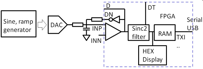
Figure 1: Structure of the sigma-delta analog to digital converter.
III. IMPLEMENTATION
To get an analog signal (without use of an expensive signal generator) which is both precise and in sync with the sampling of the ADC, a digital signal is produced by the FPGA and converted by a DAC.
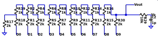
Figure 2: Schematic of the R2R digital to analog converter.
A. 10 Bit R2R DAC
For the DAC, a simple R2R converter was built. It is
basically a voltage divider consisting of resistors of 1
and 2 kΩ . The schematic and the finished structure can
be seen in Figure 2 and 3. Here it is important to note
that the resistors are precise, especially for the higher
order bits, to get a sufficient resolution.
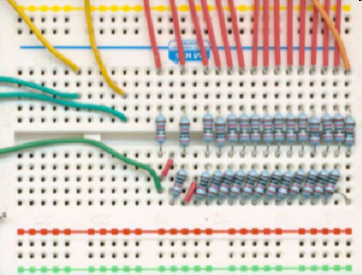
Figure 3: Structure of the R2R digital to analog converter.
B. Sigma-Delta ADC
The schematic of the ADC can be seen in Fig. 4. Here
VAWG2 is the reference voltage for the comparator on
the FPGA, contact INN. VAWG1 is realized by a digital signal generated on the
FPGA which is then converted by the R2R DAC.
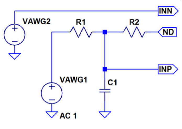
Figure 4: Schematic of the passive components of the Sigma Delta
Converter
The Value of C1 and R2 can be calculated as:
\( C \gt 12 K_{B} T \frac{2^{2B}}{V^{2}_{FS}} \)
\( R \lt\lt \frac{0.72}{B f_S C} \)
KB is the Boltzman constant, T absolute temperature, B number of bits,
vFS full scale voltage and fS signal bandwidth.
An oversampling rate of 2048 and an input bandwidth
of 6.25 kHz was chosen. This leads to an effective number of bits (ENOB) of around
\( ENOB = \frac{30 log (OSR) - 5.17 + 1.76}{6.02} \approx 15.94 \)
R1/2 and C1 were then set to a resistance of 100kΩ and
a capacitance of 22pF. The 1-Bit DAC is realized on
the FPGA which gives an analog voltage on Pin ND
connected to the summation node.
Pin INP is the second input for the comparator.
The digital Bit-stream is then fed to a SINC2 filter
with 26 Bits. It is important that the word length is long
enough and that the filter is of second order (for a 1st
order modulator). Since the serial interface has only
38400 Baud-rate and the conversion can be faster, a
dual port RAM buffer (Inst_RAM) was implemented
with a size of 2WBUFFER = 16k with 16-bit output values
taken from the upper Bits of the SINC2 filter output.
A UART is used to stream a serial output of data to
the USB port. The serial interface streams a new line
for each output data word in hexadecimal.
IV. ANALYSIS
A. Testing the R2R DAC
The R2R DAC was tested with an Electronic Explorer
Board (Digilent). A digital signal was generated and
connected to the inputs of the converter and the analog
output was then measured by the internal oscilloscope
of the board. Since the oscilloscope has only a limited
resolution of 10 bit, multiple measurements were conducted using a preamplifier.
In this way, eleven measurements with a voltage range of 300 mV each were
done to cover the whole 3.3 V output range. The testing
was done with a relatively slow ramp signal and the resulting measured values were analyzed afterwards.
Thereby, the first 10 values of each code were omitted
to avoid influences of the settling time. The remaining
values of each code were averaged and the DNL was
calculated as:
\( DNL(i) = \frac{V_{out}(i) - V_{out}(i-1) - LSB}{ LSB}\)
INL is computed by summing all DNL values up to
the current code. In Figure 5 the values of DNL and
INL can be seen.
In the resulting data, there is a unique pattern which
can be seen best in the INL graph: the data points are
quite continuous at the y axis but after a constant number of codes the values are jumping. By counting these
data clusters, we get 11 sets (first "jump" is at code 93,
second one at around 186 and so on). This cannot be
explained by inaccuracies of the resistors because then
the jumps have to be located at a code position of 2 to
the power of N (where N is between 1 and 9) or a combination of
these positions if several resistors are imprecise.
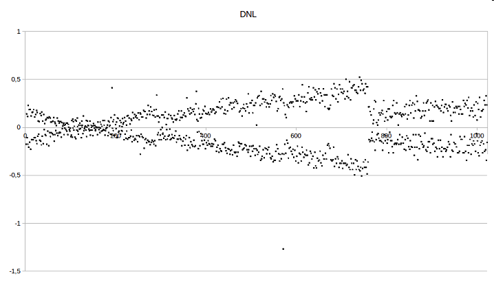
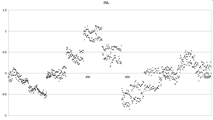
Figure 5: DNL and INL of the 10-bit R2R converter.
A reasonable explanation for this pattern is a static
gain error of the preamplifier of the oscilloscope. Having this in mind, the data values should look even better
in reality (without the measuring error) and if we assume that the values of INL (which are now above 1)
are actually within ±1, we get a DAC with a resolution
of 9 bit.
B. Testing the Sigma-Delta ADC
For the analysis, Python in combination with the
modules NumPy/SciPy and MatPlotLib were used. The
measurement was done with a digital ramp signal with
a frequency of around 2 Hz. This was chosen to have at
least one complete ramp fitting in the 16k data words
stored in the internal RAM buffer. The digital signal
was then converted by the DAC and afterwards converted back to a digital signal by the ADC. The output
values were analyzed with a histogram test.
An array with 1024 bins was computed, representing
the 1024 codes of the 10-bit converter. Afterwards, the
number of occurrence was determined. With these
numbers of occurrences, the values for DNL can be calculated as:
\( DNL = \frac{N_{i}-N_{AVG}}{N_{AVG}} \)
INL is then calculated as:
\( INL_i =INL_{i-1} + DNL_{i} \)
DNL and INL can be seen in Figure 6.
Figure 6: DNL and INL of the sigma delta converter.
The values of DNL are all within ±2, which is really
good considering the R2R DAC only has a resolution
of around 9 bits. INL is, however, with values between
±5 more diverse. This would mean a loss of 3-4 bit. But
with some minor adjustments this could surely be im-
proved.
To determine the signal to noise ratio and ENOB, a
FFT of a sine signal measurement was performed. To
avoid bleeding effects, it is beneficial to use a whole
number of sine periods for the FFT. In this way, it is not
necessary to apply windowing.
Furthermore, the number of periods should be a prime
number. Otherwise, the signal is sampled at exactly the
same points for multiple sine periods. In our case 43
sine periods were taken.
In Figure 7, the sine signal is shown in time- and frequency domain.
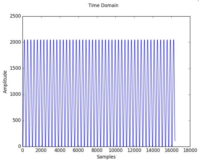
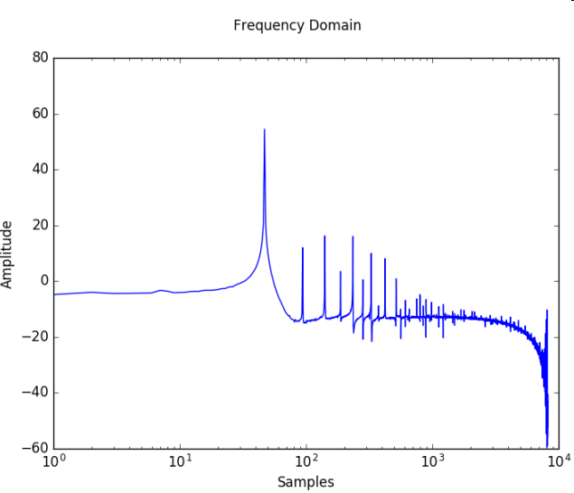
Figure 7: Converted sine signal in time- and frequency domain.
The signal frequency is represented by
the first peak of the FFT (around 43 Hz with a magnitude of 53.95 dB).
Particularly noticeable are the high
magnitudes of the harmonics. They are at around 86 Hz
(16.04 dB), 129 Hz (11.47 dB) and so on, which leads
to a total noise magnitude of 20.17 dB. By the following two equations
the Signal to Noise ratio and ENOB can be calculated:
\( SNR = 20 log \frac{V_{eff,signal}}{V_{eff,noise}} dB \)
\( ENOB = \frac{SNR - 1.76 dB}{6.02 dB} \)
The SNR can be determined as 33.78 dB which leads
to an ENOB of only 5.3 bits. The harmonics are most
likely caused by an offset error. If we assume that those
harmonics are caused by such an offset, which could be
compensated without much effort, the SNR can be in-
creased drastically. For example, if the first ten harmonics are
ignored for the noise floor calculation, the
SNR is at around 50dB. This leads to an increased
ENOB of 8 Bit.
V. CONCLUSION
The sigma delta ADC built with the NEXYS3 FPGA
board was a success. Although the resolution is not per-
fect yet, it could be improved to 8 bits with some minor
adaptations. Even with limited time and equipment, it
was possible to build and test a fully functioning sigma
delta analog to digital converter.
REFERENCES
[1] Guessab, S., P. Benabes, and R. Kielbasa, "Passive Delta-
Sigma Modulator for Low-Power Applications,"
MWSCAS'04., Feb. 2004:295-298
[2] A. Roy, M. Meza, J. Yurgelon and R. J. Baker, "An FPGA
based passive k-delta-1-sigma modulator," 2015 IEEE 58th
International Midwest Symposium on Circuits and Systems
(MWSCAS), Fort Collins, CO, 2015, pp. 1-4.
[3] Baker, R. Jacob, CMOS Circuit Design, Layout, and Simula-
tion, Third Edition, Wiley-IEEE Press, 2010.
[4] A. Roy and R. J. Baker, "A passive 2nd-order sigma-delta
modulator for low-power analog-to-digital conversion," 2014
IEEE 57th International Midwest Symposium on Circuits and
Systems (MWSCAS), College Station, TX, 2014, pp. 595-598.

| Martin Knauer received the academic degree B. Eng. in electrical engineering and information technology from the University of Applied Sciences Kempten in 2015 and will be finished with his masters in electrical engineering in 2018. Currently he is working at the University part time as a research associate. |

| Dr. Ing. Joerg E. Vollrath received 1989 his Dipl. Ing. and 1994 his Ph. D. in electrical engineering, semiconductor technology at the University of Darmstadt, Germany. Since then he worked for the memory division of Siemens and Infineon Technologies and Qimonda in various locations in the USA and Germany. He is now a Professor for Electronics at the University of Applied Science, Kempten, Germany. His expertise and interest lies in the field of design of analog and digital circuits, programmable logic, test, characterization, yield, manufacturing and reliability. He has published 30 papers and has currently 32 patents. |