Schaltungstechnik14 ColorimeterProf. Dr. Jˆrg Vollrath13 Operationsverst‰rker Offset current, noise Elektronik 3 Operationsverst‰rker |

|
Video der 14. Vorlesung 5.5.2021
|
L‰nge: 1:02:43 |
0:0:0 Fehler und Kalibrierung 0:8:17 Colorimeter 0:12:17 Blockschaltbild, Breakout session 0:12:52 Erkl‰rung 0:18:1 Analog Devices CN0312 0:22:28 Video 0:25:13 Blockanalyse 0:32:48 Transimpedanzverst‰rkergleichung 0:40:28 Hochpass, Pegelwandler 0:42:54 AD8271 Schaltung 0:47:48 Gleichung 0:55:12 Tiefpass 0:59:6 Erkl‰rung Signalverlauf |
Blockschaltbild Colorimeter
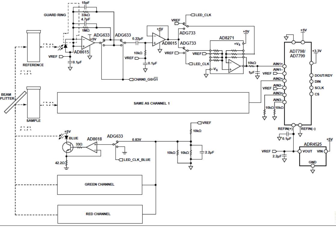
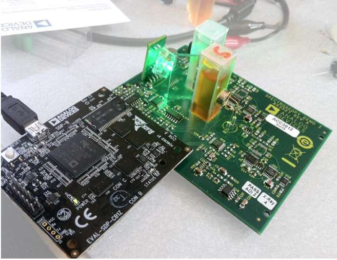
Dual-Channel Colorimeter with Programmable Gain Transimpedance Amplifiers and Synchronous Detectors (CN0312.pdf)
* OpAmp AD8615
Switch ADG633
Switch ADG733
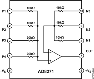
* OpAmp AD8271
OpAmp AD8618
5 kHz LED Clock
Note that the feedback capacitor, CFx, is required for stability to compensate for the pole introduced by the total input capacitance (diode capacitance plus op amp input capacitance) and the feedback resistor, RFx. For details of this analysis, see Section 5 of Practical Design Techniques for Sensor Signal Conditioning.
The output voltage of the photodiode amplifier swings between 2.5 V and 5.0 V.
For the 33 kOhm range, this 2.5 V output span corresponds to a full-scale photodiode current of 75.8 µA.
For the 1 MOhm range, it corresponds to a full-scale photodiode current of 2.5 µA.
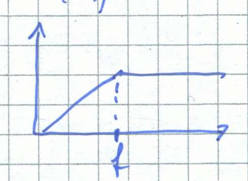
The next stage is a simple buffered ac-coupled filter. The cutoff frequency of the filter is set at 7.2 Hz.
2016
Application Note Analog Devices
CN0312 Dual-Channel Colorimeter with Programmable Gain Transimpedance Amplifiers and Synchronous Detectors
Video:
Video
2020 Nachfolgeprodukt
Analog Devices CN0363 Dual-Channel Colorimeter 24.3.2020
Video
Aufgabe
- Schaltungsanalyse: Blˆcke, Formeln
- Ðbertragnungsfunktionen
- LED Strom
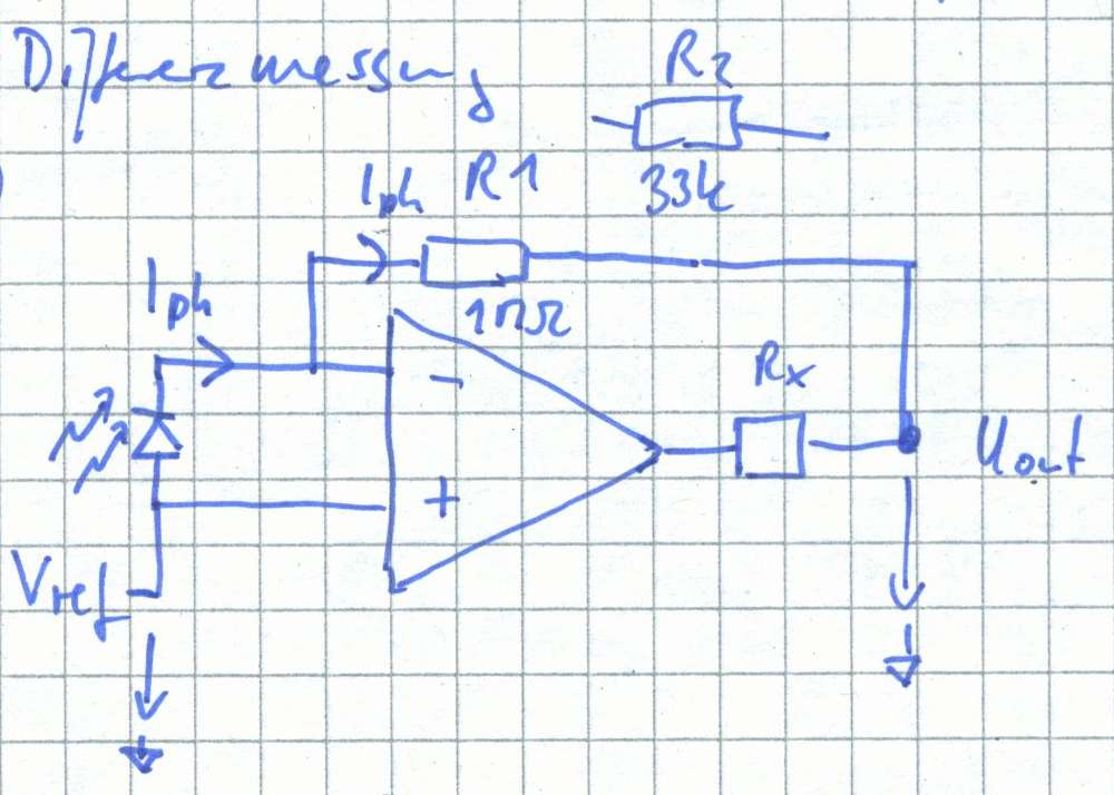
TIA AmplifierR1 = 1 MOhm, VDD = 5V, Vref = 2.5 V Uout(IPh) = - IPh · R1 + Vref \( I_{Phmax} = - \frac{U_{out} - V_{ref}}{R_1} = - \frac{V_{DD} - V_{ref}}{R_1} = - \frac{2.5}{10M \Omega} = 2.5 \mu A \) |
|
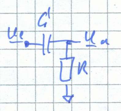
HochpassC = 0.22 µF, R = 10 kΩ \( \frac{\underline{U_a}}{\underline{U_e}} = \frac{R}{\frac{1}{j \omega C} + R } = \frac{j \omega C R}{1 + j \omega C R } \) \( f = \frac{1}{2 \pi C R } = 72.3 Hz \) |
|
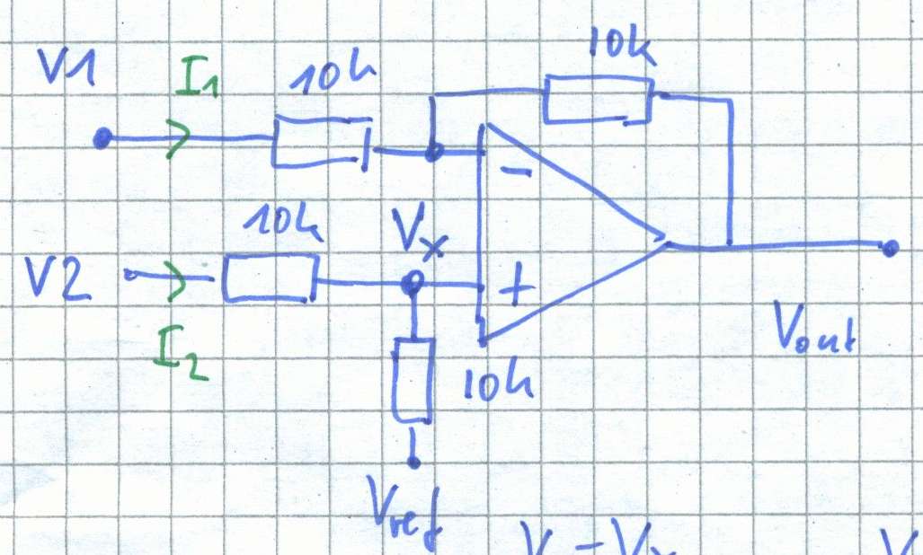
AD8271\( V_x = \frac{V_2 - V_{ref}}{2} + V_{ref} \) \( V_x = \frac{V_2}{2} + \frac{V_{ref}}{2} \) \( \frac{V_1 - V_x }{R} = I_1 = \frac{V_x - V_{out} }{R} \) Vout = 2 Vx - V1 Vout = V2 + Vref - V1 Schalterstellung 1 (hoher Pegel Vin): Vout = Vin + Vref - Vref = Vin Schalterstellung 2 (niedriger Pegel Vin): Vout = Vvref + Vvref - Vin = 2 Vvref - Vin |
|
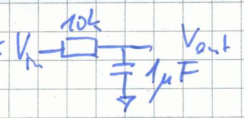
TiefpassC = 1 µF, R = 10 kΩ \( \frac{\underline{U_a}}{\underline{U_e}} = \frac{\frac{1}{j \omega C}}{R + \frac{1}{j \omega C}} = \frac{1}{1 + j \omega C R } \) \( f = \frac{1}{2 \pi C R } = 15.9 Hz \) |
|