| Hierarchy | Memory | Cost per Bit | Speed | Density |
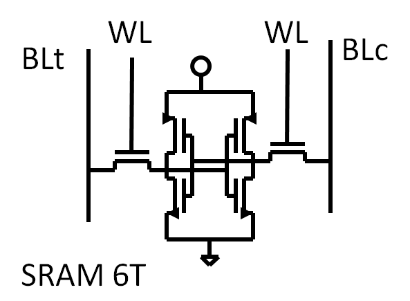
| L1 Cache | SRAM |
highest

lowest
|
fastest
slowest
|
32 kB; 128kB |
| L2 (L3) Cache | SRAM |
512 kB; 512kB (4MB) |
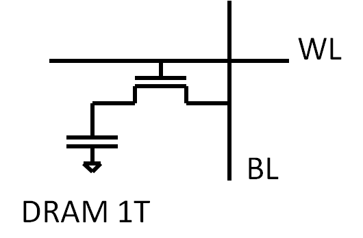
| Main Memory | DRAM |
16 GB; 4..64 GB |
| Flash Memory (SD Card) | NAND |
4 GB; 16 GB..1 TB |
| Hard Disk Memory | Magnetic/Flash |
4 TB/2..16 TB |
Cache: Intel Celeron (Core) 2007; Intel Core i3-7300 (Kaby Lake, 2017, 14nm)
Simulation
CLK high activates switches to select a memory cell and read and write
Sequence Op,Addr,Data: R,0,0; W,1,1; W, 4,0; R,0,0;
R,E,1; R,E,1; R,4,0; R,1,1; R,0,0;R,0,0
Verz÷gerungszeit 4ns von der steigenden CLK Flanke bis zum Datum.
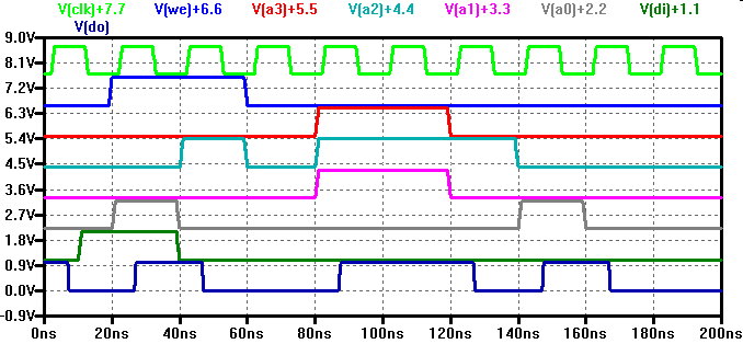
Da es 10 CLK high Zeiten gibt werden 10 Operationen durchgef³hrt.
Diese sind oben aufgelistet: R,1,0
Lesen einer "0" an der Addresse 0.
Jede Operation dauert 20ns.
Bei den Leseoperationen kann man die Zugriffszeit
zwischen CLK rising und do-─nderung sehen.
Durch die Schreib- (W), Leseoperation (R) ³berpr³ft man die Speicherung
der Information in der Zelle.
VHDL-Code: ROM
library ieee;
use ieee.std_logic_1164.all;
use ieee.numeric_std.all;
entity ROM_INSTANZIIERUNG is
   generic(ADDR_RANGE: integer:=4;
           DATA_WIDTH: integer:=8);
   port (ADDRESS : in std_logic_vector(ADDR_RANGE-1 downto 0);
         DATA : out std_logic_vector(DATA_WIDTH-1 downto 0));
end ROM_INSTANZIIERUNG;
architecture VERHALTEN of ROM_INSTANZIIERUNG is
type ROM_TYPE is array (0 to 2**ADDR_RANGE -1) of std_logic_vector(DATA_WIDTH-1 downto 0);
constant ROM : ROM_TYPE :=
   (x"0F",x"0E",x"0D",x"0C",x"0B",x"0A",x"09",x"08",
	 x"07",x"06",x"05",x"04",x"03",x"02",x"01",x"00");
begin
   DATA <= ROM(to_integer(unsigned((ADDRESS)));  -- Lesezugriff
end VERHALTEN;
VHDL-Code: RAM 01
entity Xilinx_one_port_ram_sync is
  generic(
    ADDR_WIDTH: integer :=12;
    DATA_WIDTH: integer:=8
   );
  port (
      clk: in std_logic;
      we: in std_logic;
      addr: in std_logic_vector(ADDR_WIDTH-1 downto 0);
      din: in std_logic_vector(DATA_WIDTH-1 downto 0);
      dout: out std_logic_vector(DATA_WIDTH-1 downto 0)
    );
end Xilinx_one_port_ram_sync;

Ram_1K_by_16_0: Xilinx_one_port_ram_sync
  generic map(ADDR_WIDTH=>10;DATA_WIDTH=>16)
  port map(clk => clk, we=>we,addr=>addr,din=>din,dout=>dout);
VHDL-Code: RAM 02
architecture Behavioral of Int_Memory is
type ram_type is array (2**ADDR_WIDTH-1 downto 0) of
std_logic_vector (DATA_WIDTH-1 downto 0);
signal ram: ram_type:= (others => (others => '0'));
Begin
process(clk)
begin
if ((clkæevent) and clk=æ1æ) then
if (we =æ1æ) then
ram(to_integer(unsigned(addr))) <= din;
end if;
dout <= ram(to_integer(unsigned(addr)));
end if;
end process;
end Behavioral;
DDR3 SDRAM Access
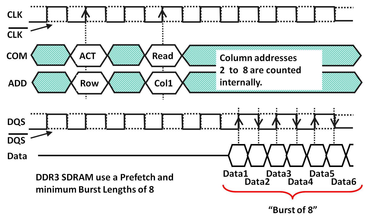
Cycle time:
Latency:
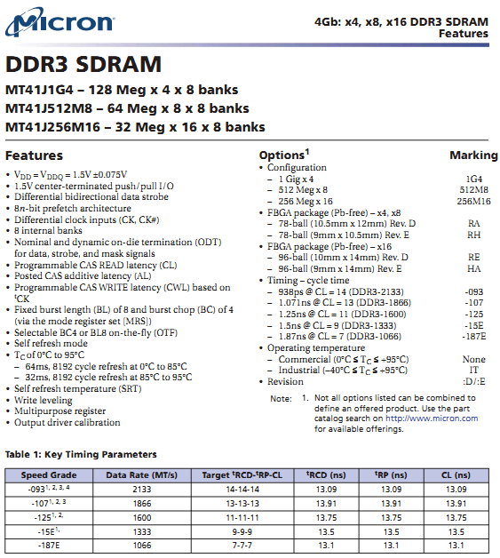
DDR3 Datasheet
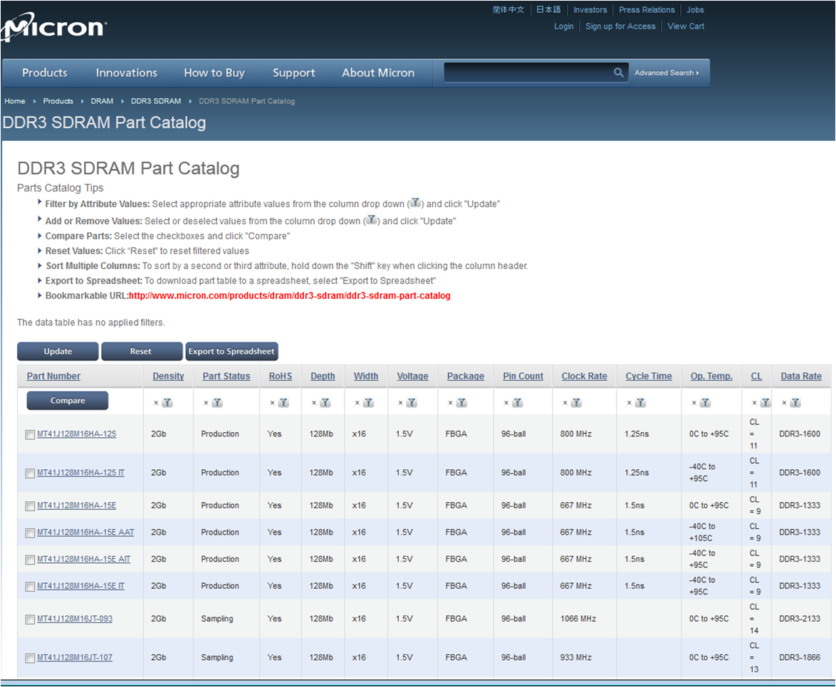
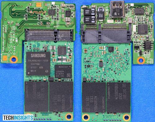
DRAM memory manufacturer: Samsung, Hynix, Micron
DDR3 Datasheet Details
Size 128Meg x 4 x 8
Power supply 1.5V
Data Rate: memory transfers per seconds 2133MT/s
Latency:
13ns+13ns
TRCD+CL
Externes DRAM, Flash sehr gro▀
|
|
Aufgaben 01
Es soll ein 64MBit Speicher mit 8 Datenleitungen realisiert werden.
Wie viele Adressleitungen werden ben÷tigt?
Ein Digitalbaustein hat 4 Eingõnge, ein Register mit 4 Bit Speicherzellen
und 5 Ausgõnge. Wie viele Tests oder Zeilen der Zustandstabelle (Vektoren)
brauchen Sie, um die logische Funktion des Bausteins vollstõndig zu testen?
Aufgabe 02
a) Erstellen Sie die Zustandstabelle f³r folgenden VHDL Code.
b) Wie viele Eingõnge, Ausgõnge und Speicherzellen werden damit realisiert?
entity ThisCircuit1SS2013 is port (
    a: in  STD_LOGIC_VECTOR (1 downto 0);
    b : in  STD_LOGIC;
    y: out  STD_LOGIC;
    clk: in STD_LOGIC);
end ThisCircuit1SS2013;
Aufgabe 02 a
Erstellen Sie die Wahrheits-/Zustandstabelle.
architecture Behavioral of ThisCircuit1SS2013 is
 signal xy:STD_LOGIC;
begin
 PROCESS (clk)
 BEGIN
  if (clk='1' and clk'event) then
    CASE a IS
      WHEN "00" => xy<=xy and b;
      WHEN "01" => xy<=a(0) or b;
      WHEN "10" => xy<=b and xy;
      WHEN "11" => xy<=a(1) and b;
      WHEN OTHERS => xy<='0';
    END CASE;
  end if;
 END PROCESS;
 y <= xy or b;
end Behavioral;
Aufgabe 02 b
Zeichnen Sie das Zeitverhalten.
 constant Tp : time := 10 ns;
   clk_process :process
   begin
  clk <= '0'; wait for Tp/2;
  clk <= '1'; wait for Tp/2;
   end process;
   stim_proc: process
   begin
      a <= "11"; b <='1';  wait for Tp;
      a <= "10"; b <='0';  wait for 2*Tp;
      a <= "00"; b <='1';  wait for Tp;
      a <= "01"; b <='0';  wait for Tp;
      a <= "11"; b <='0';  wait for Tp;
   end process;
Fragen und Diskussion
- Wozu ben÷tigt man grosse Speicherbausteine?
- Warum gibt es verschiedene Speichertypen?
- Wie sind Speicher aufgebaut?
- Warum gibt es bei Speicherbausteinen X, Y und Bank Addressen?
- Was begrenzt die maximale Gr÷▀e von Speicherbausteinen?
|
|
13 MP3 Player LFS
DRAM, SRAM, Flash, Memory Array, Volatile Memory, Cache, Hard Disk Memory, SDRAM,
Latency, Burst, Samsung, Micron, VHDL 'generic' Deklaration, VHDL Zahlenzuweisung
|