Hochschule Kempten      
Fakultät Elektrotechnik      
Elektronik 3       Fachgebiet Elektronik, Prof. Vollrath      

Elektronik 3

22 Analog-Digital-Wandler

Prof. Dr. Jörg Vollrath


21 Digital-Analog-Wandler


Video der 23. Vorlesung 12.1.2022


Länge: 1:02:43
0:0:45 Digital Analog Wandler R2R

0:3:10 LTSPICE Simulation

0:5:30 Widerstandsänderungen und Fehler

0:10:5 ADC Architekturen

0:12:6 AD Signalkette

0:19:55 Dual Slope Schaltungsanalyse

0:23:2 Simulation

0:26:53 Ein Schalter mit Transistoren

0:31:3 Zeitmessung mit Zähler

0:33:32 Rechnung Dual Slope, Schaltspannungen

0:38:37 Stromgleichung

0:42:17 Vergleich mit LTSPICE

0:44:6 Integrator

0:50:56 Gleichung des ADC

0:55:32 Schnelligkeit, Bandbreite

0:58:32 1 GHz Zähler,

1:1:25 Anzahl Bits und Frequenz

1:4:32 Flash ADC

Übersicht


Reinhold: Kap 17, 342-347

ADC architectures, resolution and conversion rate

A graph with x axis frequency and y axis resolution shows applications.

Pipeline ADC: 8..16 Bits, 1MHz..4GHz
SAR ADC: 8..18 Bits, 20kHz..8MHz
Sigma Delta ADC: 12..24 Bits, 4Hz..40MHz
Source: QUINTÁNS et al.: METHODOLOGY TO TEACH ADVANCED A/D CONVERTERS, IEEE TRANS. ON EDUCATION, VOL. 53, NO. 3, AUGUST 2010

Investigation of distributer Digikey (01/2017):
Flash ADC (Results: 366): 10 Bit 50 MSps, Range 3..16Bit, 50kHz..26GHz
     8 Bit 50kHz AD782 ADI, 3Bit 26GHz HMCAD5831LP9BE ADI, 8 Bit 1GHz MAX104CHC Maxim 16 Bit 166kHz AD7884AQ ADI
Pipeline ADC (Results: 3237): 12 Bit 125MSps, Range 6..16 Bit, 94k..2.6GHz
     12 Bit 94kHz MAX1253BEUE+, 12 Bit 2.6GHz ADI, 6 Bit 90MHz MAX1011, 16 Bit 1GHz ADS54 TI
SAR ADC (Results: 8973): 12 Bit 1MSpS, Range 8.. 32Bit 1kSps..500 MSps
     32 Bit 1MSps LTC2508 $16, 24 Bit 2MSps LTC2380 $54, 20 Bit 1.6 MSps MX11905 $30 8 Bit 500MSps ISLA118P5 Intersil $50, 8 Bit 3MSps MAX 11116 $2
Sigma Delta ADC(Results: 1928): 24 Bit 256kSps Range: 8..32 Bit , 3Sps..3.2GSps
     16 Bit 3.2GSps(100MHz) AD6676 ADI $200, 16 Bit 160MSps(2.5MHz) AD9262 ADI $48, 12 Bit 3.3kSps ADS1015 TI $2, 32Bit 1MSps LTC2508 $17
Dual Slope (Results: 28): 15 Bit 30Sps

AD conversion signal chain

Analog signal
Preamplifier (range adjustment, impedance matching)


Anti-alising filter


Sampling


Quantization


Digital coding (error correction, filter)


Digital output

Zählverfahren, Dual-Slope-Verfahren

  • Integrator
  • Schalter
  • Schmitt Trigger
  • Zähler
    Nicht dargestellt

\( C = \frac{Q}{U} = \frac{I dt}{dU} = \frac{\frac{U_{in}}{R} dt}{dU} \)
\( t_1 = \frac{C dU R}{U_{in}} \)
\( t_2 = \frac{C dU R}{U_{ref}} \)
\( \frac{t_2}{t_1} = \frac{U_{in}}{U_{ref}} \)
\( U_{in} = \frac{t_2}{t_1} U_{ref} \)

Eine Kapazität C im Integrator wird abwechselnd mit Vin geladen und mit Vref entladen.
Je nach Höhe der Spannung Vin ändert sich die Zeitdauer für einen Lade- Entladevorgang.
Ein Zähler kann diese Zeit messen.
Dieses Verfahren wird bei Multimetern verwendet.

Wie gross ist der Eingangsspannungsbereich?
Vin in V123456
t1 in ms3.859534.231524.769595.61642 7.1409310.7025

Flash ADC

Operation


Resolution B


Speed


Power

cmosedu_models.txt
The Flash ADC generates a thermometer code.
Thermometer codeBinary Code
T6T5T4T3T2T1T0 B2B1B0
0000000 000
0000001 001
0000011 010
0000111 011
0001111 100
0011111 101
0111111 110
1111111 111

For each level one comparator is needed. High count of comparators, high input capacitance.
High resolution requires low comparator offset and high gain to generate a full level digital signal.

Number of BitsMaximum OffsetGain
40.0625 · Vref 16
80.004 · Vref 256
100.001 · Vref 1024
120.0025 · Vref 4048

The offset of a comparator depends on the size of the CMOS input transistors:
Voffset ∝ \( \frac{1}{\sqrt{W \cdot L}} \)

Lower noise means higher area and higher input capacitance.

If the requirement for comparator offset is not met or noise is present sparkle codes can happen.
The thermometer code is corrupted having more than one transition from 0 to 1.

Correct code: 000000011111111Encoded binary code1000
Sparkle code: 000000010111111Encoded binary code1110
The code for the first '01' transition is 'OR'ed with the code of the second '01' transition.
Additional digital circuit can be required.
Comparators can feedback noise to the reference voltage ladder. Capacitive coupling between comparator output and intput.

SAR ADC: Blocks


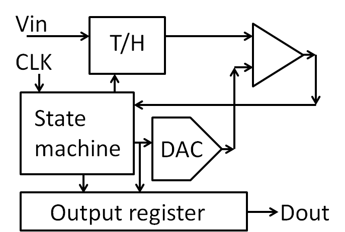
At the beginning of the conversion an input signal is sampled.
The comparator compares it with the output of the DAC.
The state machine sets the MSB depending on the outcome of the comparison and then tries the next bit.

SAR ADC: Flow, Algorithm, Simulation

Vref = 1V
Vin = 0.6 V

Stellen Sie den zeitlichen Verlauf der internen Vergleichsspannung Vout des SAR ADC dar.

Input: 0.6

1 * 0.5 + 0 * 0.25 + 0 * 0.125 + 1 * 0.0625 + 1 * 0.03125 + 0 * 0.015625 + 0 * 0.0078125 + 1 * 0.00390625
0.59765625

SAR ADC: Flow, Algorithm, Simulation

Set MSB to 1:
100000
Loop until LSB set:
Compare DAC output with analog input:
If DAC output > analog input reset current bit.
Try and set next bit.
End Loop

Blue line shows analog input voltage.
Green shows output of internal DAC.
Red shows output code with MSB first.

Input: 0.6
1 * 0.5 + 0 * 0.25 + 0 * 0.125 + 1 * 0.0625 + 1 * 0.03125 + 0 * 0.015625 + 0 * 0.0078125 + 1 * 0.00390625
0.59765625

SAR ADC: Benefits and Challenges

Mittelwertbildung

Mittelwertbildung Formel: y[i] = (x[2 * i] + x[2 * i +1]) / 2

Der Wertebereich verdoppelt sich.

Das Signal-Rausch Verhältnis ändert sich, da nur noch halb so viele FFT Frequenzen zur Verfügung stehen.
\( 20 log \left( \sqrt{2} \right) = 10 log \left( 2 \right) = 3 dB \)

Das letzte Bit hat einen Rauschanteil.


Man kann auch von einer Oversamplingrate OSR von 2 sprechen.

Der Signal-Rausch-Abstand erhöht sich bei Mittelwertbildung mit OSR Werten um:
\( 10 log \left( OSR \right) \)

Die Grafik zeigt ein Sinussignal mit einer Amplitude von Ua = 128 und einer Auflösung von 8 Bit und eine Mittelwertbildung.
Der Effektivwert ergibt sich bei einer Sinusspannung mit dem Faktor \( \sqrt{2} \).

\( A_{signal} = 20 \cdot log_{10}(\frac{Ua}{\sqrt{2}}) \)

\( A_{signal} = 20 \cdot log_{10}(\frac{128}{\sqrt{2}}) = 39 dB \)

Man erwartet ein SQNR = 6.02 * 8 dB + 1.76 dB = 49.78 dB

Das wäre ein Rauschpegel von - 10.78 dB (Grüne Linie).

Dieses Rauschen wird auf alle dargestellten Frequenzen (128 = 256 / 2 = NFFT / 2 ) aufgeteilt.

\( v_{Ges} = \sqrt{N \cdot v_i^2 } \)

\( dA_{NFFT} = 20 \cdot log_{10} \left(\sqrt{\frac{NFFT}{2}}\right) = 10 \cdot log_{10}\left(\frac{NFFT}{2}\right) = 21 dB \)

Das Rauschen der einzelnen Frequenzen liegt dann in etwa bei -31 dB (Rote Kurve).
Bei der logarithmischen Darstellung der Frequenz liegen die Punkte der höheren Frequenzen dichter zusammen. In der Darstellung sieht man eine starke Schwankung der einzelnen Werte.
Eine Ablesung des Signal-Rausch Verhältnisses aus der Graphik ist deshalb nicht sinnvoll.
Der Signal-Rausch Abstand muss numerisch berechnet werden.

Oversampling ADC: History

Nyquist ADC


Oversampling


fCLK = OSR · 2 · fbw

Clock frequency is much higher than bandwidth.

Pulse count Modulation (PCM)


Predictive Coding


Quantize difference of the signal

Sigma delta converter


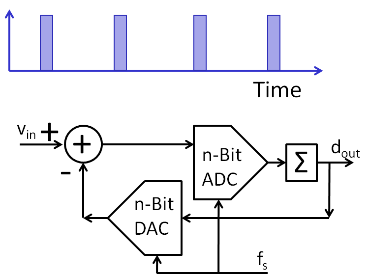
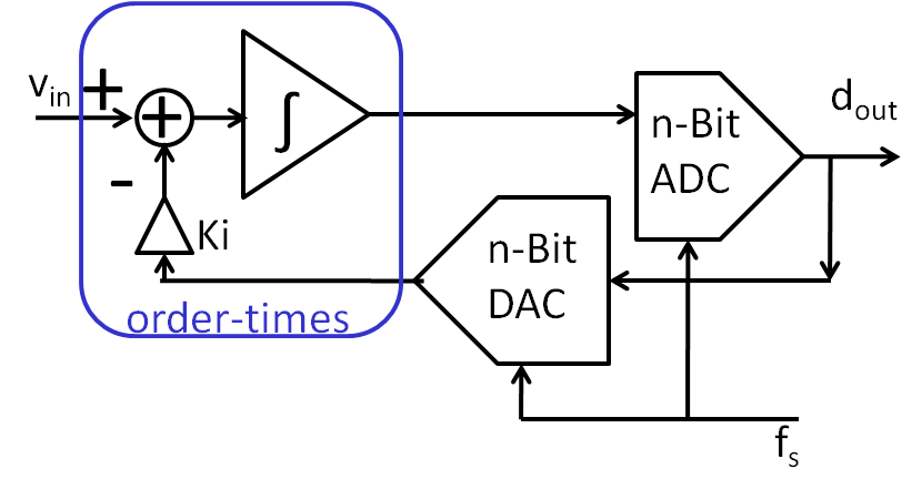
Sigma Delta ADC Architectures

  • 1st order passive Sigma Delta Converters
  • 2nd order active Sigma Delta Converters
  • Higher order active Sigma Delta Converters
  • Mashed Sigma Delta Converters

  • Signal to noise ratio
  • Transfer function and stability
  • Voltage range preventing saturation


  • Digital signal processing: filter, decimation


First order passive Sigma Delta Modulator

Internal voltage levels:

The voltage V(INT n+1) at clock cycle n+1 is:

\( V_{int n+1} = V_{int n} + \frac{\delta t}{C} \left( \frac{ V_{not(Dout)} - V_{int n}}{R} + \frac{V_{in} - V_{int n}}{R} \right) \)
\( V_{int n+1} = V_{int n} + \frac{\delta t}{C \cdot R} \left( V_{not(Dout)} + V_{in} - 2 \cdot V_{int n} \right) \)

\( \delta t \) is the period of the clock.
\( V_{Dout} \) in a real logic circuit is 0V or VDD.

These equations are used for a high level simulation.
High level simulation: 1st order sigma delta simulation

Since Vint has to stay between 0V and VDD:
\( \frac{\delta t}{C \cdot R} 2 V_{DD} \lt V_{DD} \)
\( C \cdot R \gt \frac{2}{f_{sample} } \)
\( \frac{1}{C \cdot R} \lt \frac{f_{sample} }{2} \)
The bandwidth limit of RC has to be smaller than fsample/2.
The bandwidth limit of RC has to be greater than the interested bandwith. fsample/2/OSR
\( 2 \pi f_{bw} \lt \frac{1}{C \cdot R} \lt \frac{f_{sample} }{2} \)
On the left the difference of V(in) and V(D) is integrated and then compared with V(CMP). The comparator operates with the clock frequency and gives for each clock cycle a new value.
A simple passive first order sigma delta converter uses resistors and capacitances.
This circuit is according to Baker, "CMOS integrated cicuits", Figure 6.4

Schalter und Sample and Hold


  • Widerstand des Schalters
  • Kapazitives CLK übersprechen
  • Speicherkapazität
  • Operationsverstärker

Vergleich der Wandlerprinzipien


Dual-slope Verfahren


Flash ADC


SAR ADC


Sigma Delta ADC


Zusammenfassung und nächste Vorlesung


Nächstes Mal