Hochschule Kempten      
Fakultät Elektrotechnik      
Elektronik 3       Fachgebiet Elektronik, Prof. Vollrath      

Elektronik 3

21 Digital-Analog-Wandler

Prof. Dr. Jörg Vollrath


20 Kennwerte Datenwandler


Video der 21. Vorlesung 22.12.2021


Länge: 1:02:43
0:0:0 Datenwandler Charakterisierung

0:2:12 FFT und Sinussignal

0:7:0 10 log(NFFT/2)

0:8:55 Klassifizierung: Nyquist, Oversampling, Subsampling

0:14:0 FFT Simulator

0:16:5 R String DAC

0:23:15 R2R DAC

0:26:40 Berechnung

0:28:30 VD1 und VD0 addieren

0:32:30 Gesamtgleichung

0:35:30 LTSPICE Simulation

0:37:30 Settling time

0:39:52 Widerstandsänderung

0:43:30 Kalibrierung

0:45:50 C2C DAC

0:56:20 Beispielrechnung

Übersicht


Reinhold: Kap 17, 355-360

3 Bit R string or ladder DAC

A R ladder divides VREF voltage into all possible voltage levels.
Inherent monotonic

Example:
Input Code [d2 d1 d0] = 011
LSB = Vref/8
Vout = LSB * (0*4 + 1*2 + 1) = 3/8 Vref

3 Bit R string or ladder DAC

Speed

Time constant:
Ideal voltage source at a series RC low pass.
R = (3 R || 5 R) = 15/8 R
Maximum resistance for half VDD, code 100...

Power

Static
\( P_{RS} = \frac{V_{ref}^2}{R \cdot 2^{B}} \)

Number of bits

Resistance range:
1 Ω .. 1 MΩ
20 bits.
Resistance for MOSFET switches and contacts.

Complexity

2B resistors and 2 * 2B switches are a high element count
τ = 0.25 · 2B R C
There are 2B of unit resistors.
The highest resistance is at midpoint. Half resistance will be connected to VDD and half to ground.
For equivalent resistance these resistances are in parallel.

R2R DAC

Only R and 2R values are needed.

Calculation of output voltage with equivalent sources:
R is 1 kΩ.
All data inputs can be looked at as voltage sources VD0...VD3.
The voltages internally for equivalent sources are V0L..V2L, VoutL.
\( V_{0L} = V_{D0} \frac{2 R}{4 R} = V_{D0} \frac{1}{2} \)
\( R_{i0} = 2 R || 2R = \frac{2 R 2 R}{2 R + 2 R} = R \)
\( V_{1L} = (V_{0L} - V_{D1}) \frac{2 R}{4 R} + V_{D1} = V_{0L} \frac{1}{2} + V_{D1} \frac{1}{2} = V_{D0} \frac{1}{4} + V_{D1} \frac{1}{2}\)
\( R_{i1} = 2 R || 2R = \frac{2 R 2 R}{2 R + 2 R} = R \)

\( V_{nL} = (V_{(n-1)L} - V_{Dn}) \frac{2 R}{4 R} + V_{Dn} = V_{(n-1)L} \frac{1}{2} + V_{Dn} \frac{1}{2} = \sum_{i=0}^{n} \frac{V_{Di}}{2^{n-i+1}} \)
Capacitors can be used instead of the resistance R giving a C2C DAC.

C2C DAC


Was sind Vorteile und Nachteile eines C2C DAC?
Only C and 2C values are needed.

Wie berechnen Sie die Ausgangsspannung?

Was passiert bei einem Gleichspannungssignal?

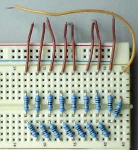
Beispiel eines R2R DAC

Der Widerstand R2 wurde auf 2.5 kΩ geändert.
Berechnen Sie die Ausgangsspanungen.

Äquivalente Quellen und Zusammenfassen:
R2 = 2.5k Die Dateneingänge sind ideale Quellen VD0...VD3.
\( V_{0L} = V_{D0} \frac{R0}{R0 + R1} = V_{D0} \frac{1}{2} \)

\( R_{i0} = R0 || R1 = \frac{R0 R1}{R0 + R1} = R0 \)

\( V_{1L} = (V_{0L} - V_{D1}) \frac{R2}{R2 + R5 + Ri0} + V_{D1} = (V_{0L} - V_{D1}) 0.45 + V_{D1} \)

\( V_{1L} = 0.56 \cdot V_{0L} + 0.44 \cdot V_{D1} \)

\( R_{i1} = R2 || (Ri0 + R5) = \frac{R2 * (Ri0 + R5) }{R2 + Ri0 + R5} = 1.1 R0 \)

\( V_{2L} = (V_{1L} - V_{D2}) \frac{R3}{R3 + R6 + R_{i1}} + V_{D2} \)

\( V_{2L} = (V_{1L} - V_{D2}) 0.486 + V_{D2} \)

\( V_{2L} = 0.486 V_{1L} + 0.514 V_{D2} \)


R2R DAC


Realer R2R DAC

8-Bit

Zusammenfassung und nächste Vorlesung


Nächstes Mal