- Projektpraktikum Elektronik
SoSe 2026 Projektpraktikum: Elektroniklabor
Prof. Dr.-Ing. Jörg Vollrath
Das 4 SWS Modul behinhaltet 1 SWS Projektmanagement. Die praktische Tätigkeit findet in 180 min Blöcken pro Woche statt.
Bitte führen Sie eine anonymisierte online Evaluierung durch:
Link: Evaluierung
Motivation
Ein Elektroniklabor benötigt Spannungsversorgung, Funktionsgenerator, Spannungsmesser, Oszilloskop und digitale IOs, um Schaltungen zu untersuchen und zu entwerfen.
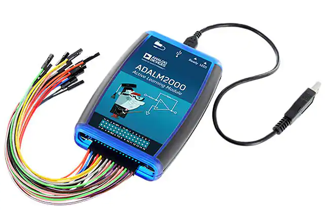
Auf dem Markt gibt es kompakte Geräte (ADALM2000, Analog Discovery, Red Pitaya, Moku Go) die einige dieser Funktionen vereinigen.
Eine ideale preisgünstige Variante mit allen Funktionen, 4 Kanal Oszilloskop, minimaler Software Installation und schönem Userinterface ist nicht erhältlich.
Dieses Praktikum beschäftigt sich damit eine vorhandene preisgünstige Open Source Realisierung weiter voran zu treiben.
Dies ist ein Projektpraktikum mit 3 SWS begleitet von 1 SWS Projektmanagment.
Es werden Gruppen zu jeweils 4 (3) Studierenden gebildet.
Ein Block mit 180 min stehen mit Betreuung pro Woche zur Verfügung.
Am Ende wird eine Präsentation und ein Bericht bewertet.
Status
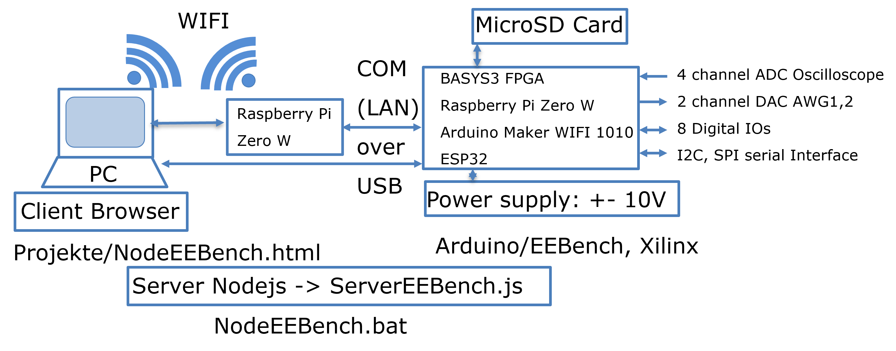
The current status of hardware and software is shown first:
Research Summary
Installation Instructions
The project is available at github JVollrath NodeEEBench.
The current version can be download as zip file NodeEEBenchV20261302.zip.
Unpack the files into "C:\temp". All files should then be in the directory "C:\temp\NodeEEBench".
The subdirectories "node" and "node_modules" contain the node executable to provide a web server and connection to a serial interface.
Hardware: BASYS3
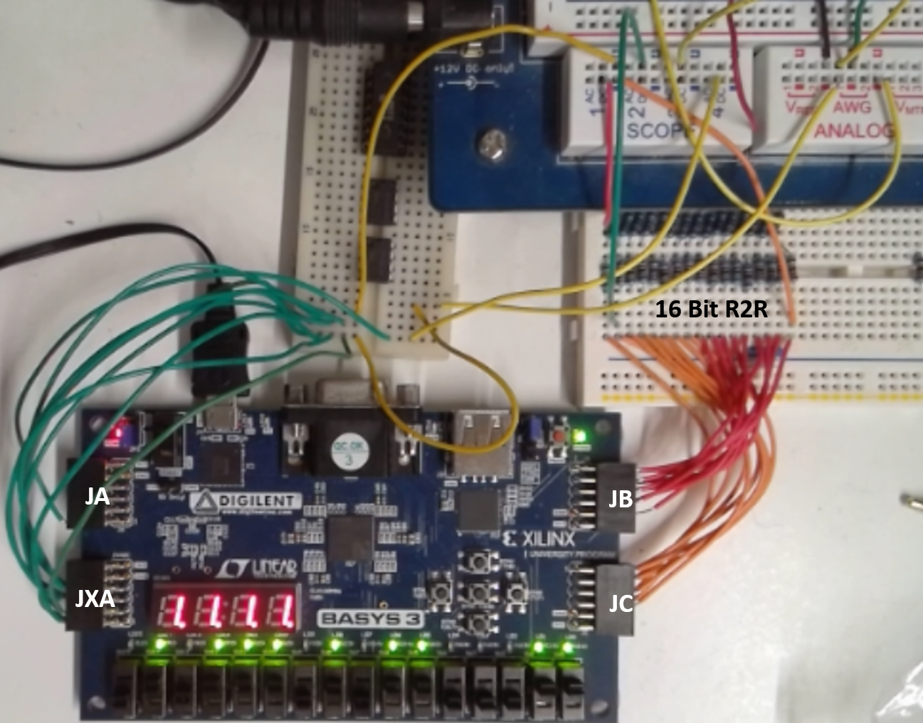
Figure: BASYS3 FPGA Board with R2R DAC and Electronic Explorer
Hardware features:
4 channel, 12-Bit, 125 kSps, 0..1 V range ADC oscilloscope FPGA (XADC)
1 channel, 16-Bit, 30kSps, 0..3.3 V range, 15us settling time, 100k,220k R2R DAC
4k samples transfered via UART with Baud rate 230400
Pins Oscilloscope: OSC1 JXA 1 in, 7 GND; OSC2 JXA 2 in, 8 GND; OSC3 JXA 3 in, 9 GND; OSC4 JXA 4 in, 10 GND;
Pins AWG: JC upper 8 Bit 10,9,8,7,4,3,2,1; JB lower 8 Bit 10,9,8,7,4,3,2,1;
16 Bit R2R DAC: left side output D15 connected to scope 1, right side D0 and GND connection.
The FPGA configuration is done using the VHDL project files in the directory C:\temp\NodeEEBench\Xilinx\EEBench.
The Basys 3 Programming Guide guides through flash memory programming.
Hardware: Arduino
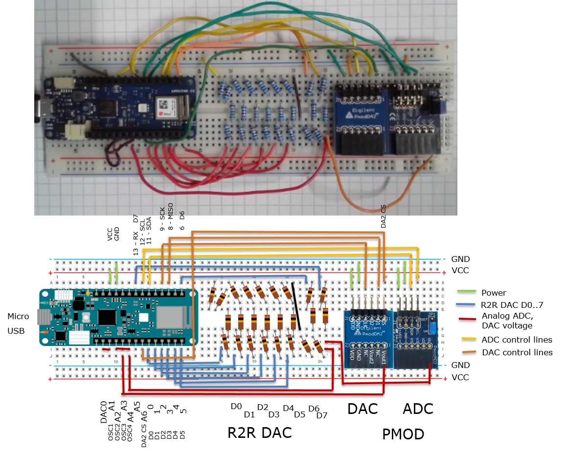
Additional ADC and DAC are realized with Digilent PMOD AD2, Digilent PMOD DA2, R2R DAC with 10k,20k resistors.
In the subdirectory Arduino are different sketches:
- "EEBench" the default configuration for NodeEEBench.bat.
- "DataConverterCharV4" realizes an R2R DAC for data converter investigation StartServerAx.bat.
Detailed description is available at Interface Electronics ADC DAC Analysis Laboratory - "DataConverterCharV5" realizes an serial C DAC for data converter investigation StartServerAx.bat.
Low cost serial DAC simulation, realization, error correction and characterization - "DataConverterCharSerialSAR" realizes a serial SAR circuit.
Software: User interface
Start the program with "C:\temp\NodeEEBench\NodeEEBench.bat".
A command window is started, the serial communication with a BASYS3 or Arduino board established and a web browser connects to "localhost:3000" to display the graphical user interface.
Besides the standard interface started with "C:\temp\NodeEEBench\NodeEEBench.bat" There is an additional special Arduino Interface for INL, DNL and SNR, FFT operation, which can be started with "C:\temp\NodeEEBench\StartServerAx.bat"
Detailed description is available at Interface Electronics ADC DAC Analysis Laboratory
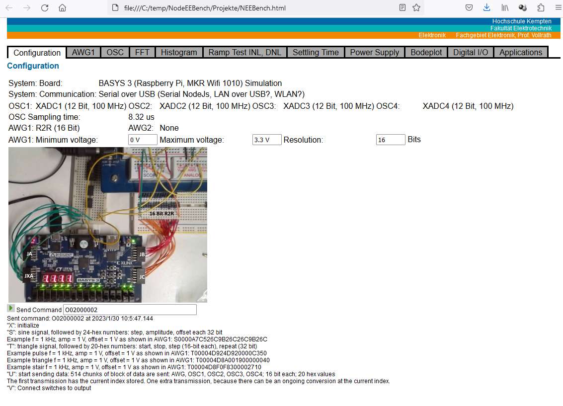
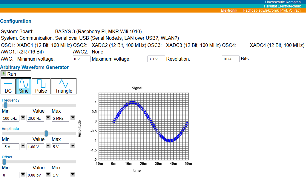
Figure: Configuration and signal generator user interface
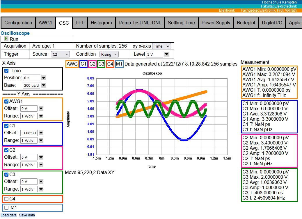
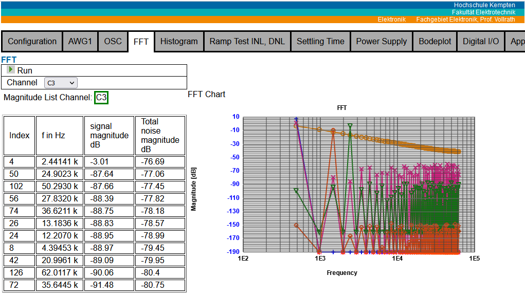
Figure: Oscilloscope and FFT interface V05
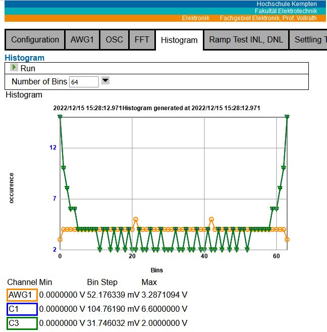
Figure: Histogram interface V06
Software features
Configuration with individual serial command transfer.
AWG: DC, stair, triangle and sine generator with frequency, amplitude and offset
OSC: 4 channel and AWG with 8..4096 sample selection, xy display, voltage and code selection, rising, falling single channel trigger, minimum, maximum, average, amplitude, period and frequency calculation.
There is voltage sample data and code data display available. A measured signal can be directly compared to the golden AWG signal in voltage or code.
FFT: AWG1, OSC1, OSC2, OSC3, OSC4 with highest magnitude frequencies and total noise magnitude for ENOB, SINAD, SFDR, SDR calculation.
Histogram with adjustable (16..256) number of bins.
Ramp Test INL, DNL
Lookup Table
Software architecture
The 3 main files are shown in the upper picture and listed here.
NodeEEBench.bat: Starting batch file
ServerEEBench.js: Javascript file for node js to create server and start communication
Projekte/NodeEEBench.html: Main user interface delivered by the nodejs server
Configuration for Arduino in folder Arduino/EEBench.
Configuration for BASYS3 FPGA in folder Xilinx/EEBench.
The folder 'Documentation' contains further information.
Unique features (Work in progress)
Signalgenerator DAC and Oscilloscope ADC integer value display.
Lookup table application for arbitrary waveform generator.
Oscilloscope data processing and feeding output to arbitrary waveform generator.
Serial interface data processing.
ADC, DAC, INL, DNL analysis.
Vorgehen 2026
- Sichten und Inbetriebnahme des vorhandenen Materials.
- Transfer auf CMOD A7
- PMOD DA2, PMOD AD2, MCP4728 DAC, I2C/SPI Digital Interface Page, SRAM Memory Buffer
- Präsentation der Ergebnisse
- Projektbericht
Planen Sie ihre Aktivitäten und überprüfen Sie ihren Projektfortschritt.
Sichern Sie Teilergebnisse durch geeignete Versionierung.
Zielsystem
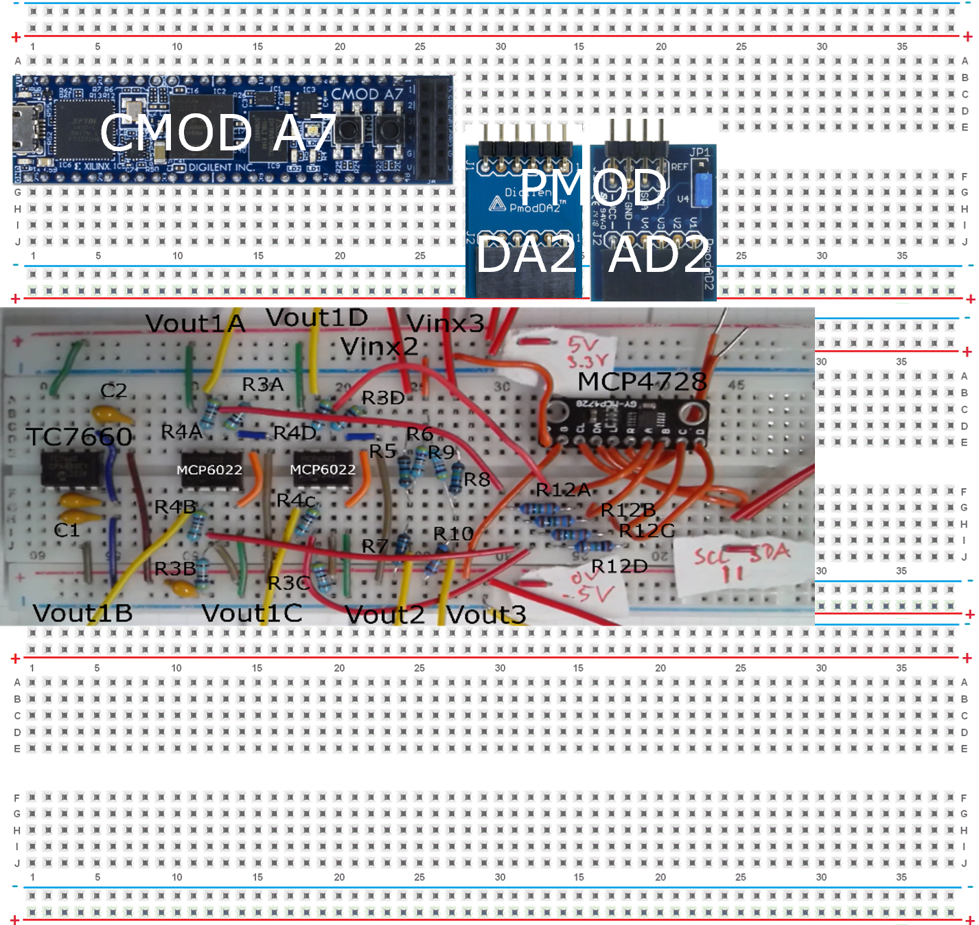
Figure: Target breadboard configuration of CMOD A7
Das Endergebnis ist eine Pappbox mit 2 oder 3 Breadboards.
1 oder 2 Breadboards realisieren das 4 Kanal Oszilloskop (PMOD AD2), den 2 Kanal Signalgenerator (PMOD DA2) und eine Spannungsversorgung VP+, VP-, Vref1,2 (MCP4728, TC7660S, MCP6022, R2R).
Die Eingangs- und Ausgangsspannungsbereiche werden durch Spannungsteiler und Operationsverstärkerschaltungen erweitert.
Interface und Power Dokumentation
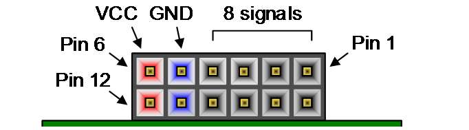
Ein PMOD Anschluss könnte die Signal bereitstellen:
Tabelle: Analoge Schnittstelle
| 6 | 5 | 4 | 3 | 2 | 1 |
| VCC | GND | OSC4 | OSC3 | OSC2 | OSC1 |
| VR1 | GND | VP- | VP+ | AWG2 | AWG1 |
| 12 | 11 | 10 | 9 | 8 | 7 |
Es kann noch eine I2C, SPI PMOD Schnittstelle und eine digitale IO PMOD Schnittstelle geben.
Das extra Breadboard wird die zu untersuchende Schaltung enthalten, passt in die Pappschachtel und bleibt leer.
Components:
CMOD A7 control circuit USB
PMOD DA2 AWG1,2
PMOD AD2 OSC 1,2,3,4
TC7660S negative voltage -VDD
MCP6022 rail-to-rail OpAmp
output range conversion
voltage buffer
R-voltage divider
C-buffer caps
MCP4728 VP+, VP-, Vref1,2
(USB3 PD module +10V? -> TC7600 -10V)
Projekt Ideen
- Umsetzung mit A7 CMOD FPGA
- Systematische Beschreibung von Test und Inbetriebsnahme
- Inbetriebnahme anderer Mikroprozessoren
RaspberryPi Zero, Infineon uP, TI uP, STMicro uP - Unterstützung weiterer Datenwandler: ADC, DAC
- Implementierung einer Spannungsversorgung
- Implementierung digitaler IOs und Busse (I2C, SPI, UART)
- Implementierung von Steuerung und Regelung
- Software
Test, Dokumentation, Modularisierung, Open Source, Github, Versions - Anwendungsfälle
Bauelementemessung, Datenwandler, Motorsteuerung, Ladungspumpe, Operationsverstärker, Sample and Hold, Duty Cycle Regler für Buck Converter, Schaltungen, Graphical Interface um SAR Steuerung zu implementieren - Features
Tracking, Priorisierung, Test, Hardware/Software matching - Second waveform generator AWG2
Bauteile
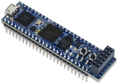
- A7 CMOD
- BASYS3 FPGA
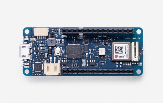
- Arduino MKR WIFI 1010
- Raspberry Pi Zero W
- (Infineon, STMicro, TI MSP3240 Mikroprocessor board)
- Datenwandler PMODs: Digilent DA1, DA2, AD1, AD2; MAX
- Power supply
List?? Analog devices Eval, TI Eval board - Schaltungsbauteile
- Power ICs
Bauteile
BASYS3 Board
Arduino MKR WIFI 1010
RaspberryPi Zero W2
A7 CMOD
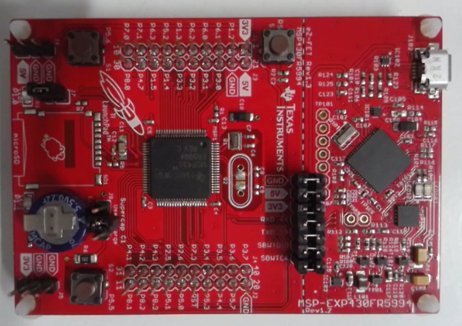
TI MSP3240
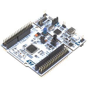
ST Micro Nucleo
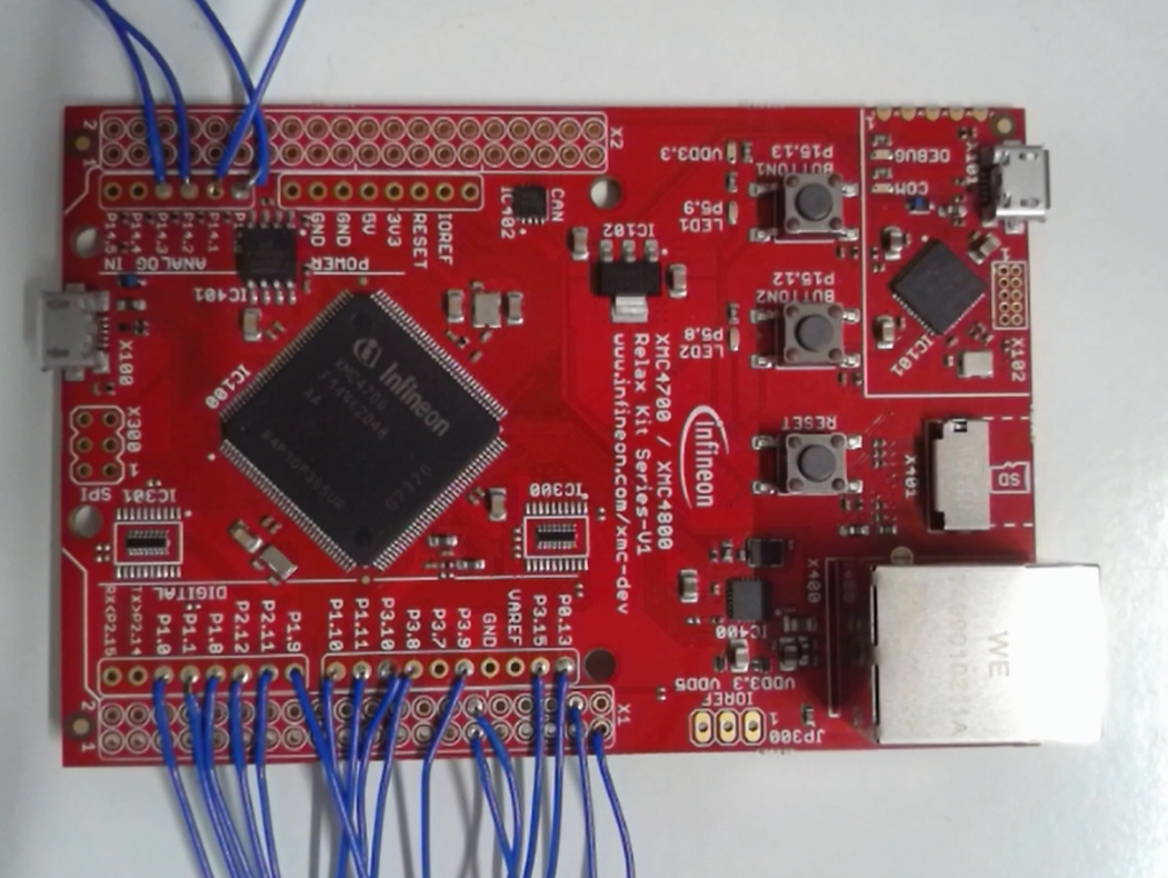
Infineon XMC4700 Relax
PMOD ADC, DAC
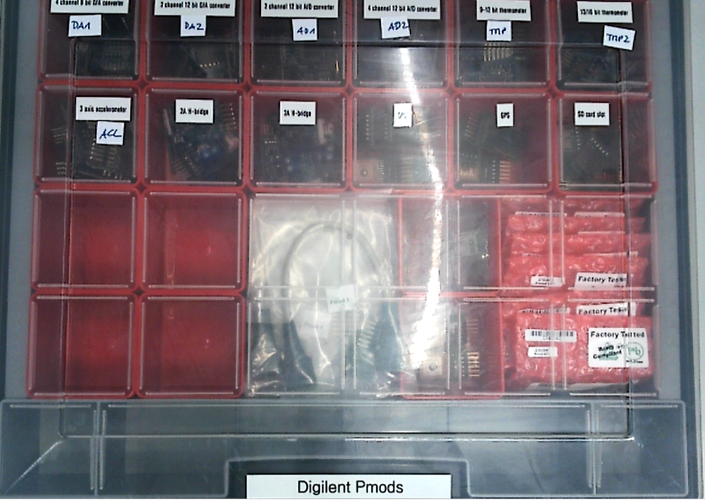
Digilent
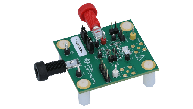
LM27762EVM
Geräte
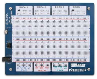
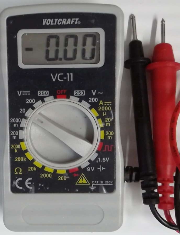
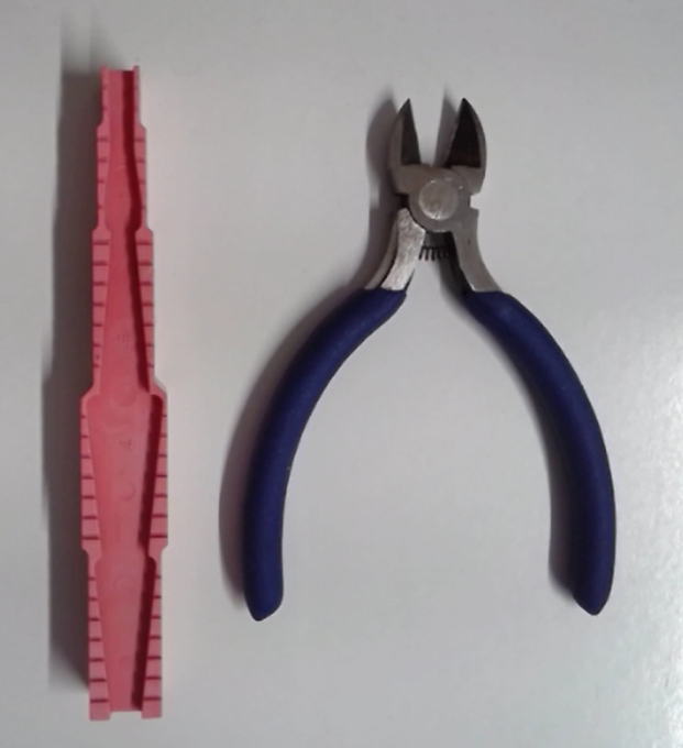
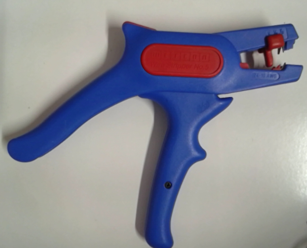
Breadboard, Electronic Explorer, Multimeter, Seitenschneider, KomponentenabbiegevorrichtungBreadboard
Electronic Explorer
Multimeter
Seitenschneider
Abisolierer
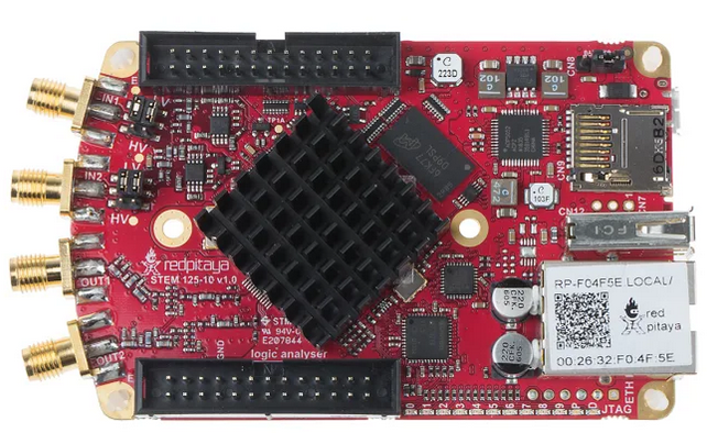
ADALM2000
Red Pitaya
Progress 2026
11 Termine a 180 min entsprechen 3 SWS in 15 Wochen
12.07.2026 So Abgabe Ausarbeitung
- Ein Dokument einer Gruppe mit Namen gekennzeichnete Abschnitte oder separate Dokumente
- Wie bekommt man einen leichteren Einstieg?
Was waren die größten Herausforderungen? - Anleitung wie man den Code einfügt und testet
- Dokumente per Email als pdf
- Zip Datei / Github der hdl, xdc Dateien mit Erläuterung der Dateinamen (Dateiliste)
- Informationen zur Bachelorarbeit
23.06.2026 Di 11:45 11 Präsentation
- Eine Gruppe präsentiert nach der Anderen.
Jedes Gruppenmitglied hat ca. 5 min Zeit. - Es gibt Fragen und Diskussion nach jeder Gruppenpräsentation.
- Die Präsentation trägt einen kleinen Teil zur Note bei.
Bewertung des Leistungsbeitrag der Gruppenmitglieder untereinander.
Bewertung der individuellen Präsentation.
Bewertung der Gruppenleistungen.
Skala: (++),+,0,-,(--)
Projekt Selbstbewertung
2.06.2026 10 Debugging of I2C and SPI interface
19.05.2026 09 VHDL Implementation and Simulation
- CMOD A7 implementation shows no response to U command in terminal window
- More help and instructions how to structure the project needed
- Oscilloscope Auto set used a lot. It takes a lot of time and shows no signal. With an expectation of voltage level and frequency manual setting would be possible.
- There are many VHDL versions of an implementation available.
- Discussion about dealing with downloaded code:
Simulation, line by line understanding, implementation in given project or stand alone better?
Isn't it similar to given code in digital electronics laboratory?
There are multiple good options available how to deal with the problem - Operation of NodeEEBech for measuring PMODS commands still difficult:
Sharing conflict between nodeJS server and Arduino IDE of COM port
Arduino stuck and not operational any more
Pick signals and time base for measurement with oscilloscope
Activation of AWG, oscilloscope or power tab
Power tab is used to supply MCP4728 commands.
Sends commands only with change in value and needs a button for continues sending of one channel for debugging to get a repetitive oscilloscope signal
12.05.2026 08 VHDL Implementation and Simulation
- Vivado lost XADC block
- Oscilloscope reads ADC, shows sometimes steps in the waveform
and frequency is sometimes ok
repetitive saving of same value in buffer memory - Debug by putting interesting signals to PMOD connections and measure with oscilloscope
- How to debug VHDL for sending MCP4728 commands
28.04.2026 07 VHDL Implementation and Simulation
- Transfering a VIVADO project
Local copy of files versus link to files - Configuring Vivado for different hardware with python
Wrapper and separate directories - inout pin using "Z"; pullup or pulldown resistor needed
Change speed limit with resistor value? - Debugging with internal signals at PMOD pins
- Generating test case with state machine
- Use measured valid bus signals from Arduino transfered to state machine for testing VHDL
- Model PMOD with state machine
- Validating correct bit file with date and time stamp
- Dealing with Vivado versions (Downgrade 2019.1/upgrade latest) Python?
- Report: Instructions, background, strategy, challenges and outlook for (I2C/SPI) implementation
- Integrating new features: Identify differences, identify/run tests
If there is a good test suite adding code and features without breaking code is easy.
How to test embedded system (microcontroller, server, user interface)?
21.04.2026 06 VHDL Implementation and Simulation
- Transfer simulation to hardware difficult
Test vector state machine necessary? - Documentation samples started
- Measurement of I2C, SPI signals with Electronic Explorer leads to reset of Arduino?!
- Supporting BASYS3, BASYS3 and PMODs, CMOD A7 strategy difficult
How to set up an Vivado project for multiple hardware platforms - Attaching I2C/SPI interface to EEBench.vhdl
- Coordination of available pins for I2C and SPI, BASYS3, CMOD A7
- Understanding VHDL code is difficult.
MUX, state machine, connections
State machine needs initialization, start, finish signals for communication and synchronization with other operations - Block diagrams of VHDL with input and output signals helps understanding
State diagrams of VHDL code necessary - High frustation with VHDL syntax, Electronic Explorer and Arduino operation
14.04.2026 05 Interface Analysis, Measurement, Implementation
- Everybody has a task and contributes?
- How does the group communication work?
- Is there a time plan?
7.04.2026 04 Projektaufgaben
- Coping with difficult challenge, anxiety and unknowns.
- VHDL für das Projekt
- Measure Arduino SPI, I2C signals and identify commands and timing
- Identify commands for data converters from data sheet:
Used by Arduino, using more than 1 channel, changing to high speed communication
Compare with examples from the internet - Search internet for SPI, I2C VHDL code with test and try these solutions with simulation
Copy, paste, simulate, analyze results and analyze program - Make block diagram for EEBench.vhd
Identify registers and multiplexers for ADC, DAC control - Transfer program to CMOD A7
Compare CMOD A7 pinout to BASYS3 pinout (Basys3_Master.xdc)
How to manage 2 FPGA options? - Extensive test, verification and documentation
31.03.2026 03 Projektfindungsphase
- Parallel tasks and serial tasks, task distribution
- The data converter SPI/I2C communication is the minimum requirement
- VHDL basic SPI/I2C functionality
Simulation, measurement, implementation
Configuration of interface to data converter
Optimization, synchronization of speed (baud rate), multiplexing channels - Documentation, verification and test
- VHDL knowledge limited
Merging into code
24.03.2026 02 Projektfindungsphase
- 3 Groups, 4 persons time conflict, hardware, measurement
- BASYS3 System with Vivado VHDL project was introduced
- Hardware: 6x Arduino MKR Wifi 1010, 6x BASYS3 (CMOD A7), 6x PMODs, 6x MCP4728
- Data sheet, I2C, SPI measuremnt Arduino, Vivado Code, VHDL Code I2C, SPI
- Connecting data converters to an FPGA via SPI and I2C extending NodeEEBench project.
- Are there sufficient tasks available for 5 persons per group?
- Improvements to motivate usage of NodeEEBench
- How easy is it to start configuring BASYS 3 board.
- Document user experience challenges and satisfaction
- SPI and I2C communication with data converters
Connection, maximum speed, channel multiplexing
Measure Arduino communication signals - Make videos and/or better documentation:
System startup, attaching new hardware, FPGA/Arduino configuration, User interface change - Implement front end input/output level conversion
0 V..1 V to -5 V..5 V
17.03.2026 01 Start
- Professor and 13 students in 3 groups Tuesday 14:00-17:00
- Introduction: System block diagram with hardware and software
- Installation was done via github zip file, Arduino IDE with libraries and Vivado were installed
- Simulation and Arduino Maker WiFi 1010 was started and used with arbitrary waveform generator and oscilloscope
- Task: CMOD A7 with VHDL for SPI and I2C ADC, DAC communication was discussed
- Task: Hardware PMOD DA2, PMOD AD2, MCP4728
- Github needs short installation instructions at the main page
- Github is used at the moment as open versioned repository
Test for functionality check for check in is missing to enable pull requests in group work - Each weak at the beginning one student for each group reports status
- Each student needs a written report with contributions at the end
- There are time conflicts with other classes