Research SummaryJörg Vollrath, University of Applied Science Kempten, Germany, Joerg.vollrath@hs-kempten.deMarch, 2023 OverviewAbstract and IntroductionReview
Project
Outlook
Summary |
Abstract
Data converters are very important in electronics to convert sensor signals and drive actuators. There are many opportunities to optimize data converter circuits for speed, power consumption, accuracy and cost. A good understanding and characterization of data converters is needed.
This work introduces an open low cost platform for data converter characterization and research.
Specific signal generation and acquistion is important to realize new data converter circuits and measure performance.
This platform can also be used for general electrical engineering.
Electrical engineering needs a laboratory containing power supplies (logic, analog positive and negative, reference), arbitrary waveform generators, digital inputs and outputs, voltage and current measurements and an oscilloscope (4 channels).
This equipment should be usable as semiconductor parameter analyzer (high accuracy measurement with curent and voltage limits), spectrum analyzer (high resolution ADC), digitzer (many channels with many samples), data logger (SD-card, battery supply) and sensor actuator interfaces (I2C, SPI, PMOD, Bluetooth).
Measurement of electrical systems with IV curves, signal time behaviour and transfer functions (bode diagram) is one application.
High accuracy, high speed and low noise measurements are required for data converters and need special measurement procedures.
For prototypes serial transmission and receiving circuits, digital signal processing facilities and control blocks enable system development.
A nice web user interface and no software installation would enhance the usability.
This paper tries to develop such systems.
The current status of hardware and software is shown first:
Installation Instructions
Installation Instructions
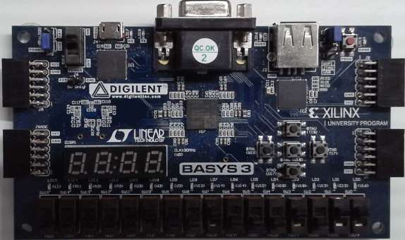
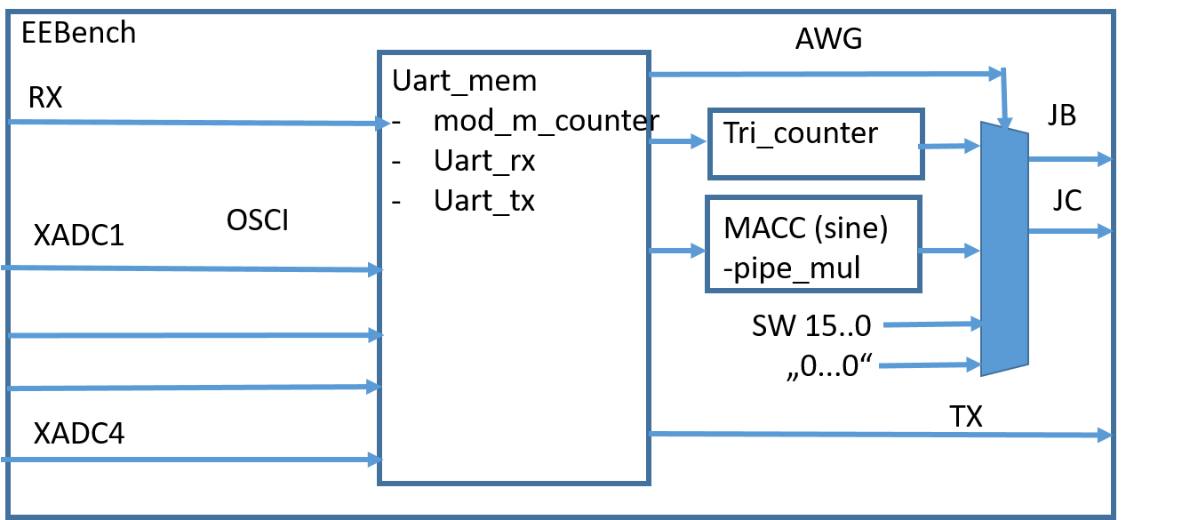
Figure: BASYS3 FPGA Board with R2R DAC and Electronic Explorer
Hardware features:
4 channel, 12-Bit, 125 kSps, 0..1 V range ADC oscilloscope FPGA (XADC)
1 channel, 16-Bit, 30kSps, 0..3.3 V range, 15us settling time, 100k,220k R2R DAC
4k samples transfered via UART with Baud rate 230400
Pins Oscilloscope: OSC1 JXA 1 in, 7 GND; OSC2 JXA 2 in, 8 GND; OSC3 JXA 3 in, 9 GND; OSC4 JXA 4 in, 10 GND;
Pins AWG: JC upper 8 Bit 10,9,8,7,4,3,2,1; JB lower 8 Bit 10,9,8,7,4,3,2,1;
16 Bit R2R DAC: left side output D15 connected to scope 1, right side D0 and GND connection.
The FPGA configuration is done using the VHDL project files:
VHDL project files EEBench_V06.zip
A nodeJS server providing the user interface and serial communication is realized in the following files:
Node.js project files with NodeEEBench.bat to start as zip V06
Figure: Configuration and signal generator user interface
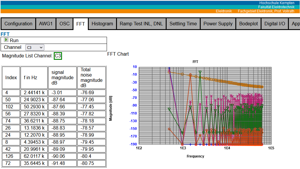
Figure: Oscilloscope and FFT interface V05
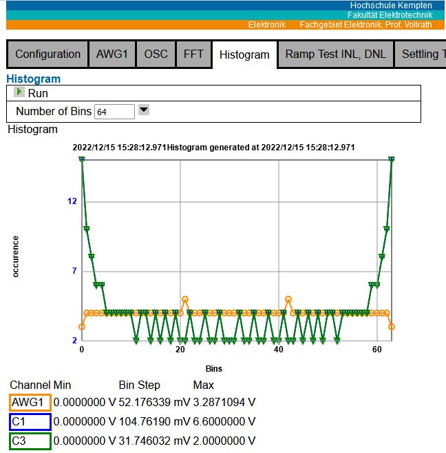
Figure: Histogram interface V06
Software features:
Configuration with individual serial command transfer.
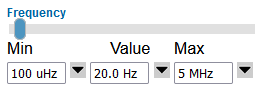
AWG: DC, stair, triangle and sine generator with frequency, amplitude and offset
OSC: 4 channel and AWG with 8..4096 sample selection, xy display, voltage and code selection, rising, falling singel channel trigger, minimum, maximum, average, amplitude, period and frequency calculation.
There is voltage sample data and code data display available. A measured signal can be directly compared to the golden AWG signal in voltage or code.
FFT: AWG1, OSC1, OSC2, OSc3, OSC4 with highest magnitude frequencies and total noise magnitude for ENOB, SINAD, SFDR, SDR calculation.
Histogram with adjustable (16..256) number of bins.
Video EEBench
|
Länge: 7:10 min |
00:0 EEBench by Joerg Vollrath
00:17 BASYS 3 Hardware
01:03 VHDL and nodejs
01:26 Vivado with EEBench, Bitstream generation
02:00 Program the device
02:36 NodeEEBench folder
03:02 NodeEEBench.bat
03:44 Browser
03:57 Arbitrary wavform WG
04:20 Oscilloscope, trigger, moving
05:03 Min, max, average, amplitude, periode,
05:20 FFT
05:43 FFT with fitting sine
06:12 Histogram
06:32 Outlook customization
06:55 Available zip files
|
This system with an arbitrary waveform generator and an oscilloscope with FFT and histogram is very low cost using a BASYS3 system for 140.- Euro (2023) and open source with a nice user interface.
It is possible to show provided AWG and sampled OSC codes and compare them.
An optimized sampling scheme could have one high speed channel and some lower speed channels.
A sampling sequence of C1,C2,C1,C3,C1,C2,C1,C4 gives a sample rate of fs for C1, f2/2 for C2 and fs/4 for C3 and C4.
A driving circuit for the AWG DAC is still missing.
A starting point for a lot of opportunities for optimization and student projects is realized with this project.
Review of data converter circuits and measurement systems
Data converter circuits
The lecture 'Interface Electronics' incorporated the following data converters in the laboratory:
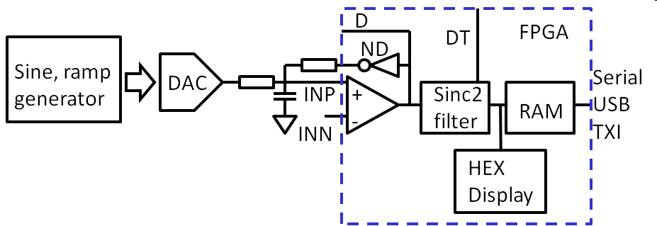 Figure: SAR, sigma delta, pipeline ADC
All these circuits are easy to realize on a breadboard with a limited number of components.
- NEXYS 3
- SAR ADC
- Sigma Delta ADC (7 Bit, 6.25 kSs, OSR 2048)
- Serial Pipeline ADC (7 (16) Bit, 10 Sps,
- R2R, C2C DAC
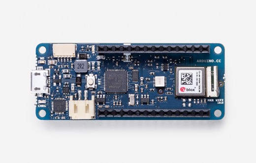
- MKR Wifi 1010
- C serial DAC
- 8 Bit, 300 Sps, R2R DAC
- 2 chan, 12-Bit, (125kHz) PMOD DA2 (20.-)
- 4 chan, 12-Bit, 1 MSps PMOD AD2 (20.-)
Buttons controlled the configuration and data was logged at the serial port.
The FPGA is needed to generate time (clock cycle) accurate control signals.
Due to the limited hardware and breadboard, only low speed and resolution data converters could be realized.
Typical ramp measurement measurements for INL and DNL and sine signal FFT measurements for SNR, ENOB could be done.
The serial data could be copied to JavaScript based HTML pages to do the analysis.
JavaScript data processing web pages and tools:
- ADC simulation of INL, DNL and spectrum analysis
- Read LTSPICE raw file for data converter analysis.
- JavaScript ADC FFT histogram data analysis application with calibration
- Digital signal generator
- Read oscilloscope data
Commercial data converter modules
An overview of commercial data converters was done to review the state of art and identify missing performance for research and potential candidates for circuits and measurement.
There are ADC and DAC modules having resolutions from 8-bit to 24-bit and sample rates between 1 kSs and 1 MSps.
It is assumed that higher speeds are not supported with the PMOD connectors.
The FPGA would support at the normal pins 100MHz at the transceivers 1GBps.
Table: ADC and DAC sorted by relevance for this project
| Converter | Number of channels | Resolution | Conversion speed | Settling sampling time | Converter Component | Component price (Euro) | Manufacturer | Board name | Board price (Euro) | Interface | Comment |
| DAC | 4 | 12 | (150 kSps ?) | 6 us | MCP4728 | 5.- | Microchip | Adafruit 4470 | 8.- | I2C 3.4MBps | Low cost |
| DAC | 1 | 12 | 1 MSps | 8us | DAC121S101-Q1 | 3.- | Texas Instruments | Digilent PMOD DA2 | 20.- | SPI 30 MHz | High speed |
| DAC | 1 | 16 | 100 kHz | 18 us | MAX5216 | 6.7 | Analog Devices (Maxim) | Maxim MAX5216PMB1 PMOD | 23.- | SPI 50 MHz | |
| DAC | 1 | 12 | 200 kSps | 6 us | MCP4725 | 7.- | Microchip | Adafruit 935 | 7.- | I2C 3.4 MBps | Low cost |
| DAC | 4 | 8 | 1.875 MSps | AD7303 | Analog Devices | Digilent PMOD DA1 | 20.- | Low cost | |||
| ADC | 4 | 12 | 1 us | AD7991 | Analog Devices | Digilent PMOD AD2 | High speed | ||||
| ADC | 6 | 24 | 16 kSps | MAX11259 | Analog Devices | Maxim PMOD | 90.- | I2C | High resolution, high price | ||
| ADC | 18 | 240 Sps | MCP3424 | 5.- | Microchip | DFRobot.com | 15.- | High resolution, low price | |||
| ADC | 16 | MAX11205 | Maxim PMOD | 18.- | SPI | ||||||
| ADC | 16 | 860 Sps | ADS1115 | 6.- | |||||||
| ADC | 4 | 12 | ADS1015 | 12.- | |||||||
| ADC | 2 | 12 | 1 MSps | AD7476A | Analog Devices | Digilent PMOD AD1 | 34.- |
There are parts missing with more than 1 MSps and more than 16 Bit.
Looking at the FPGA frequency the following sample rates should be possible:
100 MHz / 24 Bit = 4 MBps
100 MHz / 16 Bit = 6 MBps
100 MHz / 12 Bit = 8 MBps
(1 MSps, 16 Bit; 1 MSps 20 Bit; 1 MSps 24 Bit; 8 MSps 12Bit; 6 MSps 16Bit; 4 MSps 24Bit; 100kSps 24 Bit)
Data converter in applications
There are high speed data converters listed here for AWG and oscilloscope function and low speed multi channel data converters for power supply and offset control.
Since the used board has only PMOD connectors the high speed data converters were not used in this project. Most of the high speed data converters have only 2 channels, whereby experience during electronic laboratories showed the benefit of a 4 channel oscilloscope for ease of use.
ADC: 2 channel, 10-Bit, 40 MSps, ADS5204, Texas Instruments, 15.- (2 x for 4 channels) Electronic Explorer
ADC: 2 channel, 14-Bit, 105MS/s, AD9648, Analog Devices, 90.- (Analog Discovery 2)
DAC: 2 channel, 14 Bit, 275 MSps, DAC5672PFB, Texas Instruments, 25.- (Electronic Explorer)
DAC: 4 channel, 12-Bit, 125 kSps, DAC7565PW, texas Instruments, 12.- (Electronic Explorer)
DAC: 2 channel, 12-Bit, 200 kSps, DAC7552RGT, Texas Instruments, 5.- Electronic Explorer
DAC: 2 channel, 14-Bit, 200 kSps, AD5643, Analog Devices, 15.-, Interface: 50 MHz, (Analog Discovery) general
DAC: AD5645, Analog Devices, general control Analog Discovery 2
DAC: 14Bit, 125MS/s, AD9717, Analog Devices, 30.-, AWG Analog Discovery 2
ADC: Wägezellenmodul - mit ADC 24-Bit-Wandler NAU7802, Nuvoton, Adafruit 4538
ADC: 2 channel, 14-Bit, 125 MSps, LTC2145CUP-14, Analog Devices (Linear Technologies), 90.-, Red Pitaya
DAC: 2 channel, 14-Bit, 125 MSps, DAC1401D125HL, Renesas, (abgekündigt), 14.-, Red Pitaya.
Data converter systems
Some platforms use higher integrated data converters to reduce costs.
- 12-bit ADC 1 MSPS 16 channels, 4 DAC ADuC7020 40.- complex EVAL-ADUC7020MKZ
- ADC/DAC AD9963, Analog Devices, ADADALM2000 60.-
- AMC60804T 1MSps 12 chan 12 bit ADC, 4 chan 12 bit DAC, 10.-;
AMC7812B 500kSps 16 chan 12 bit ADC 12 chan
AFE88101
TI ADC/DAC https://www.ti.com/data-converters/integrated-special-function/precision-adcs-and-dacs/products.html
- PIC24EP256GP204 (PSLab)
- Waveshare Raspberry Pi AD/DA Expansion Shield Board for Adding High-Precision AD/DA Functions to Raspberry Pi Onboard
- Arduino Maker Wifi 1010
- MSP-EXP430FR5994, Texas Instruments
- PSoCT 4100S Plus, Infineon
Commercial data converter evaluation boards and software
High performance data converters are provided with evaluation boards and software to be able to verify INL, DNL, ENOB, SNR and SFDR.Typically these boards have a FPGA and high speed memory for the samples.
Reference voltage sources and a combination of DAC and ADC is required to be able to measure data sheet specified performance.
The software is proproietrary, sometimes in conjunction with Labview or Matlab and difficult to modify.
- MAX11905EVKIT, Analog Devices (Maxim) 100.- + Zedboard
- PLABS-SAR-EVM-PDK Texas Instruments 500.-
- EVAL-AD5443-DBRDZ 14-Bit DAC Evaluation Board 70.-
- ADS1256EVM-PDK 200.-; ADC: ADS1256 24 Bit 30 KSps 8 chan ADC, Texas Instruments, 10.-
- DAC80502EVM Evaluation module 50.-; DAC: DAC8552 (16 Bit, 2 chan, 10us) Sensor Interface, Texas Instruments
- EVAL-ADUC7020MKZ 30.- ARM7 MCU 32-Bit, 12-bit 1 MSps ADC up to 16 channels, 12-bit DAC up to 4 channels
Automotive and Microcontroller manufacturers (Infineon, Microchip) are also incorporating ADCs and DACs in their products.
Data Converter GUI
Typically a signal generator, a refererence voltage supply and an ADC is needed for measurement.
Offset and gain error is measured and calibrated.
Ramp measurements can be done for INL and DNL.
Sine signal measurements provide INL, DNL and with FFT SNR, SDR, ENOB, THD.
A source synchronous design using power of 2 samples and odd number of signal cycles makes measurement evaluation with FFT easier.
This functionality is implemented in hardware and GUI.
An extra feature could be software based error correction.
Error correction with a lookup table was implemented in software and simulation in the JavaScript tools:
- ADC simulation of INL, DNL and spectrum analysis
- JavaScript ADC FFT histogram data analysis application with calibration
Example GUIs with listed features from Texas Instruments and Analog Devices are shown here to present an overview.
Texas Instruments
Texas Instruments, High Speed Data Converter Pro GUI, User's Guide, SLW087D, march 2017
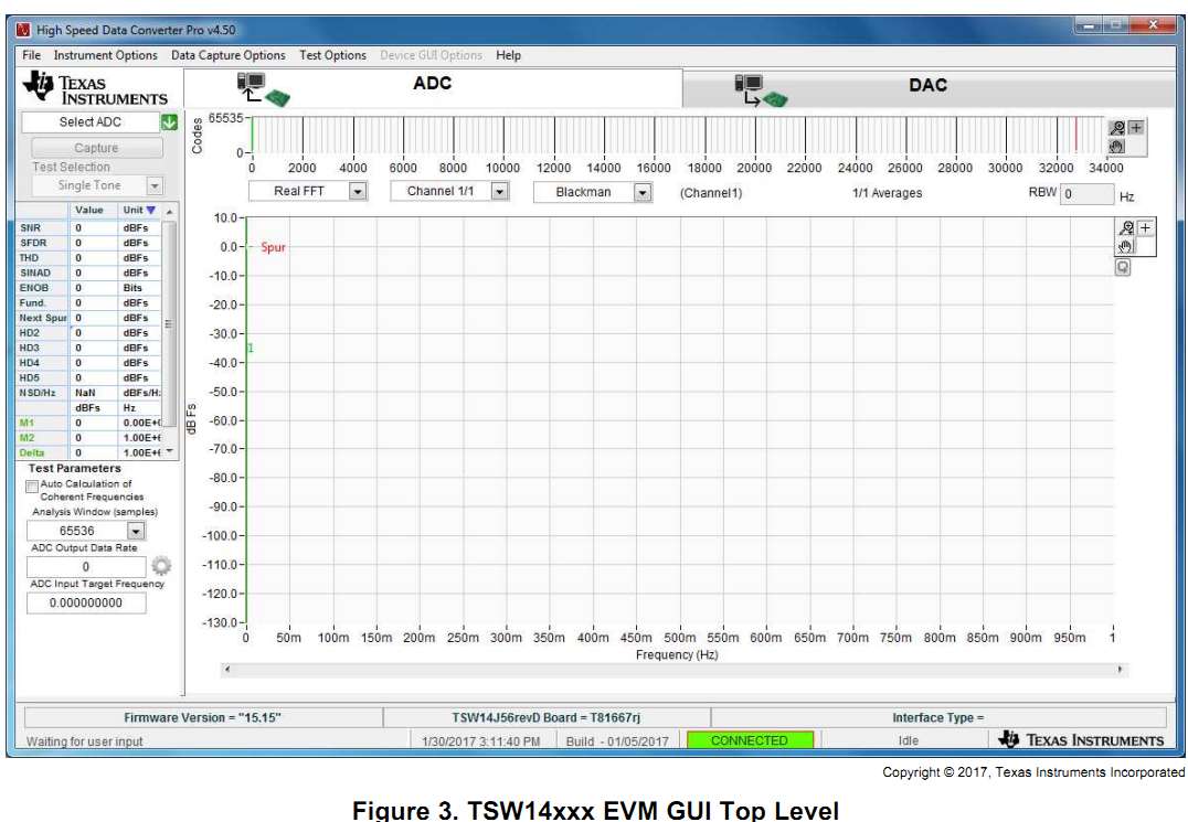
Figure: TI GUI Top level ADC
Select ADC or DAC, Small time window, large FFT window, windowing, code display, SNR, SFDR, THD, SINAD, ENOB, signal, harmonics, HD2, HD3, HD4, HD5
Samples, output data rate, input target frequency
2 channel display
Eye diagram, channel power measurement
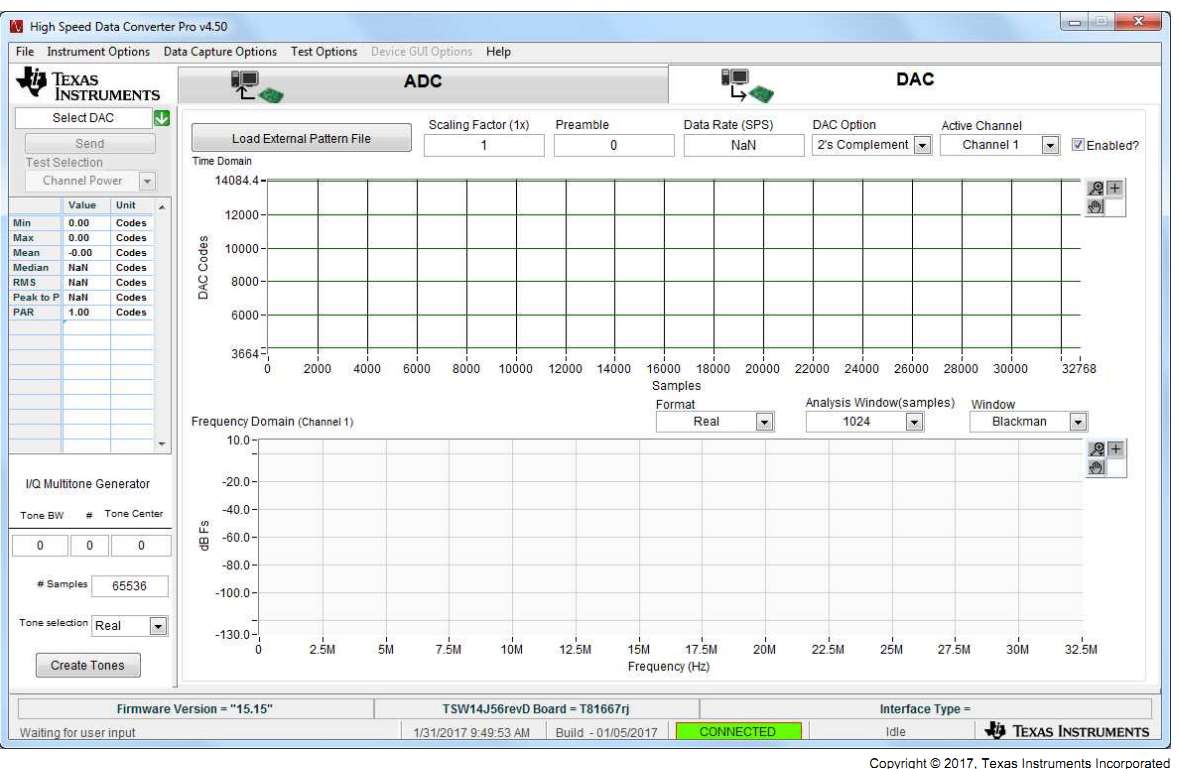
Figure: TI GUI Top level DAC
DAC vector file 16-bit, 16k or 4096..512M vectors
Multitone generator
Example for power: WCDMA_TM1_complexIF30MHz_Fdata122.88MHz_1000.csv
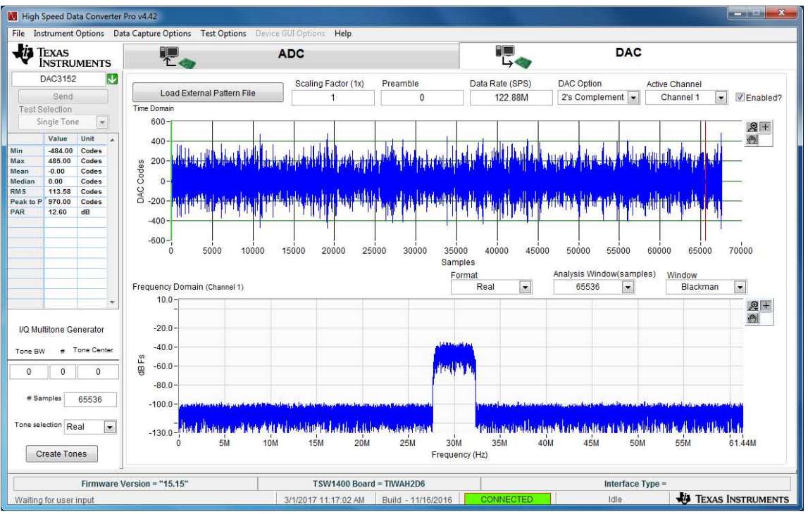
Figure: TI GUI Top level DAC Power
Analog Devices
EVAL-AD7380FMCZ/EVAL-AD7381FMCZ User Guide UG-1304
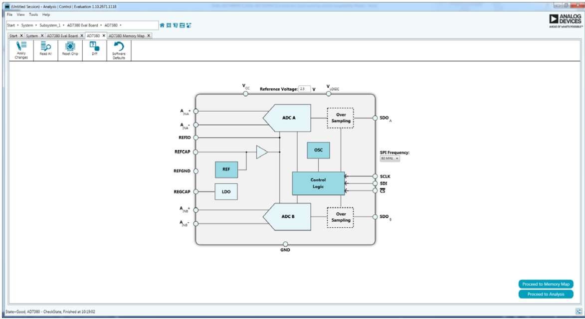
Figure: Analog Devices GUI DAC configuration
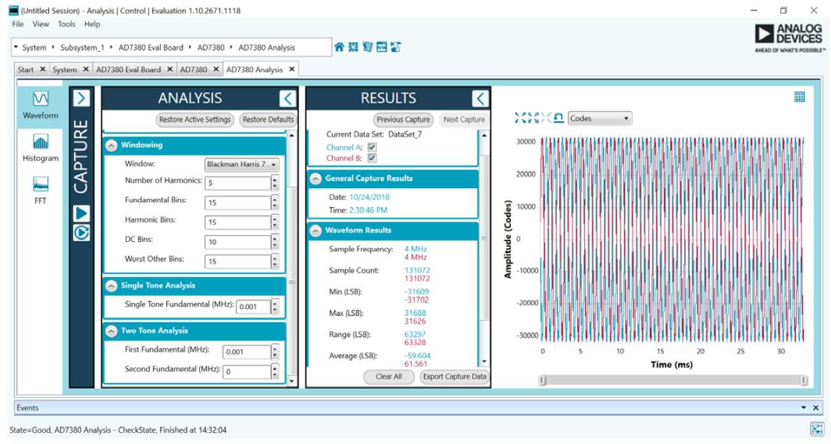
Figure: Analog Devices GUI Waveform
Universal measurement platforms
Beside special purpose data converter measurement systems there are low cost universal measurement platforms available, which are presented here and can be used for data converter measurements.
Available systems:
 |
 |
 |
 |
 |
 |
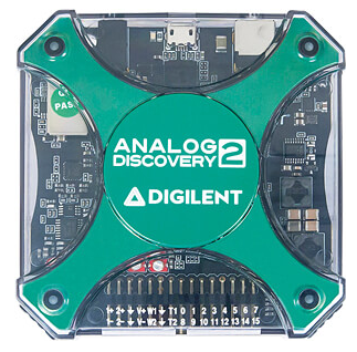
- Electronic Explorer (Digilent/National Instruments) (665 Euro, 2022, 350 Euro, 2010)
- ADALM2000 (Analog Devices) (300 Euro, 2022)
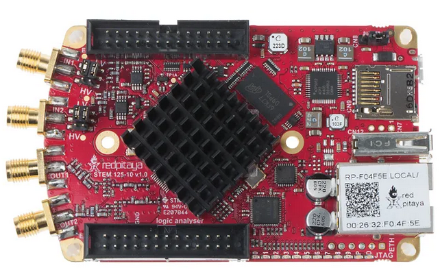
- Red Pitaya (250..450 Euro, 2022)
- Analog Discovery (450 Euro, 2022)
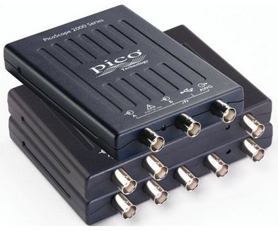
- PicoScope 2000 (100..1000 Euro, 2022)
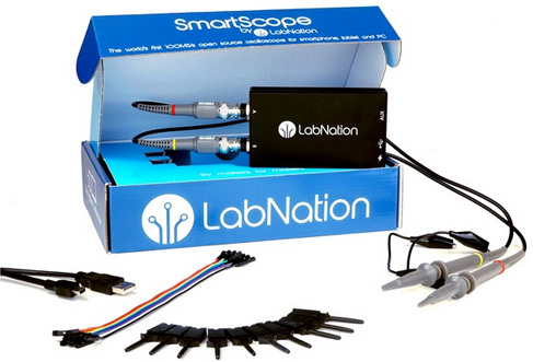
- SmartScope (270 Euro, 2022)
- PokiMeter (Very basic function)
- PSLab (Limited availability)
The Electronic Explorer has a very nice user interface, which is of no cost and can be run in a demo mode without hardware.
The ADALM2000 is very cheap, open source and has most of the functionality. It provdies a web server over USB connection, but needs a phyton install for software.
The Red Pitaya has a web interface and needs no software to be installed. Unfortunately also here a price-hike for higher precision was happened.
The Red Pitaya provides -3.3V with maximum of 50 mA.
Most of the systems provide also a very detailed hardware description (schematic).
Example: Analog Discovery circuit description
All systems provide positive and negative voltage supplies, oscilloscope, arbitrary waveform generators and digital IOs. The number of channels and the current and voltage limits vary.
The higher performance systems used FPGAs and now SoC FPGAs like the ZYNQ SoC line to control the hardware. Lower cost and performance systems use a microcontroller to realize the system.
For data converter characterization a data converter code (not voltage) based control should be available and digital data of the AWG should be easily available.
There seems to be room for low cost open source systems with adaptable functionality for use as electronics laboratory similar to the popularity of the Arduino, ESP32 or Raspberry Pi microprocessors.
FPA or microprocessor based systems could be used for low cost lower performance laboratory systems.
Characterization and measurement procedures for data converters and general electronics
Typically applications of an electronics laboratory are listed here.
Applications can be an audio amplifier with microphone and speaker, filters, buck and boost converters, charge pumps, data converters, and motor control
Static IV curve (Transistor, Diode, Opamp)
Example: Bipolar transistor: UBE, IB (2 OSC channels), UCE, IC (2 OSC channels)
High current source with current limit IC
Low number of measurement points
Sine signal circuit analysis (amplifier, filter)
Positiv and engativ power supply (OpAmp), sine signal generator (AWG1), 4 channel signal measurement
Bode plot (Opamp, filter, LC meter)
Software control: AWG1, amplitude, frequency range, phase measurement
White noise generation and FFT
Signal processing
Digital FPGA logic or MACC blocks can be used from an FPGA An AWG1 generated signal (analog, digital IO) is measured with OSC1 and fed to an analog LCR filter circuit, or a SC-filter circuit (Digital switch control signals), or digital to a microprocessor and measured with OSC2 or (calculated digital signal).
The internal signal from OSC1 can be digitally processed internally and fed to AWG2 (analog and digital IO) and measured with OSC4 to compared it with the other solutions.
Data converter characterization (offset, gain, INL, DNL, SNR, ENOB)
A triangle waveform covering all possible data converter codes is used to measure and calculate offset, gain error, INL and DNL.
A sine signal with full amplitude covering all codes and odd number of cycles during a power of 2 sample acquisition allows to do a FFT and look at signal, harmonics and noise for ENOB, SDR, SFDR, SINAD calculation.
High accuracy and a large number of samples is needed for accurate high speed measurements.
Project
After reviewing current available systems and requirements for electronic laboratory systems now an optimum system can be proposed. Proposed system overview
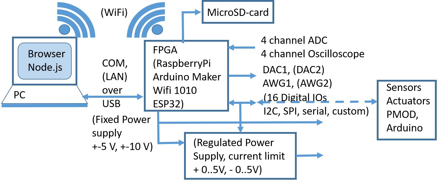
Figure: Propsed system overview
The figure shows the overview of the ideal proposed system. Functions in brackets are not implemented yet.
Basic and optimum system specification
Basic:
- 4 channel oscilloscope
- 2 arbitrary waveform generators
- Positive, negative, logic (3.3/2.5V) power supply
- 16 Digital IOs
- Breadboard with interface
- Browser based PC user interface for serial communication
Optimum:
- Web based user interface and simulation mode
- Digital IOs with digital interface (I2C, serial, SPI, gray code)
- Bode diagram
- IV curves: diode, transistor, opamp
- Data converter characterization with calibration
- Digital signal processing: filters, control elements, switched capacitor circuits
Features of BASYS 3 system and software
- System: BASYS 3 with 230400 Baud serial interface over USB
- AWG: 1 channel, 16 Bit R2R, 0..3.3V output range, 7.7 MHz sine
- OSC: 4 channel, XADC 1MSps (multiplexed x8) to 125 kHz, 0..1 V input range, up to 4k points
- The original digital code of AWG1 can be displayed as reference
- Variable buffer size is implemented
- FFT: up to 4k points signal and noise calculation, histogram display
- DAC characterization interface
- Switching between code display, voltage display
- Special trigger for ramp up test
System overview
Software installation and updating is always difficult. The best solution would be, if the system
is providing a WiFi or LAN connection via USB that can be operated via the browser.
The ADALM provides a LAN connection via USB, but there is no web interface available.
Most systems provide only a serial interface over USB. Therefore a nodejs application is built,
which can be installed to provide a web interface and talks via the serial interface to the system.
A simulation mode should enable running the system without hardware.
Hardware solutions
A suitable low cost hardware was chosen for this project looking at FPGA
and microcontroller boards.
- The original digital code of AWG1 can be displayed as reference
- Variable buffer size is implemented
- Switching between code display, voltage display
- Special trigger for ramp up test
 BASYS3 |
 CORA Z7 |
 CMOD A7 |
 Raspberry Pi |
 MKR Wifi 1010 |
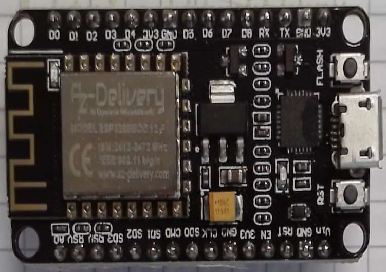 ESP32 |
Figure: BASYS3, CORA Z7, CMOD A7, RaspberryPi, MKR Wifi 1010 and ESP32
The BASYS 3 board is used for the laboratory digital electronics. In this review ALTERA FPGA boards are still more expensive then Xilinix FPGA boards.
The MKR Wifi 1010 is used for laboratory Interface electronics. Raspberry Pis and ESP32 boards are used for various student projects.
Target:
- BASYS3 FPGA (140 Euro) (CMOD A7 (SRAM) 120.- Euro)
- CORA Z7 FPGA, uP(150 Euro)
- RaspberryPi (10.- - 100.- Euro)
- MKR Wifi 1010 (35.- Euro)
- ESP 32 (12.- Euro)
FPGA Realization
Since VHDL code is more difficult than JavaScript client code as much calculation and verification as possible is put on the client side.
First the ADC implementation with the XADC is presented and then the arbitrary waveform generator for pulse, triangle, dc and sine signal.
Then the UART interface for control and data transfer is realized and commands are specified.
Extensive simulations of the circuits were done.
Finally a data buffer with control was realized.
ADC 4 Channel Oscilloscope
XADC Wizard
The XADC can sample 4 differential channels on the BASYS3 board multiplexed.
Input range is 0..1V.
Sampling is done at 1 MSps multiplexing 4 channels.
Lower row JXADC is negative input, upper row positive input.
The FPGA has more XADC pins which can be used, but these are not carfully routed.
https://www.youtube.com/watch?v=2j4UHLYqBDI
- Basic:
- Interface Option: DRP
- Timing mode: Continous mode (always running)
- Startup Channel selection: Channel sequence
- DRP Timing options: 100MHz (Board frequency), 1000kS/s (maximum speed)
- ADC Setup
- Continous, Averaging None
- Alarms: unchecking not used
- Channel sequencer: choose channels
vaux6,7,14,15
Lower folder IP Sources: Instatiation Template: VHDL vho
Basys 3 FPGA xc7a35tcpg236-1
A file XADC_EE.xci is generated with the XADC interface.
my_adc : XADC_EE
  PORT MAP (
    di_in => "0000000000000000", -- input wire [15 : 0] di_in
    daddr_in => daddr_in,        -- input wire [6 : 0] daddr_in hex 16,17,1e,1f
    den_in => enable,            -- input wire den_in
    dwe_in => '0',               -- input wire dwe_in
    drdy_out => ready,           -- output wire drdy_out
    do_out => data,              -- output wire [15 : 0] do_out
    dclk_in => CLK,              -- input wire dclk_in
    reset_in => BTN(4),          -- input wire reset_in
    vp_in => vp_in,              -- input wire vp_in
    vn_in => vn_in,              -- input wire vn_in
    vauxp6 => JXA(0),            -- input wire vauxp6
    vauxn6 => JXA(4),            -- input wire vauxn6
    vauxp7 => JXA(2),            -- input wire vauxp7
    vauxn7 => JXA(6),            -- input wire vauxn7
    vauxp14 => JXA(1),           -- input wire vauxp14
    vauxn14 => JXA(5),           -- input wire vauxn14
    vauxp15 => JXA(3),           -- input wire vauxp15
    vauxn15 => JXA(7),           -- input wire vauxn15
    channel_out => channel_out,  -- output wire [4 : 0] channel_out
    eoc_out => enable,           -- output wire eoc_out
    alarm_out => alarm_out,      -- output wire alarm_out
    eos_out => eos_out,          -- output wire eos_out
    busy_out => busy_out         -- output wire busy_out
  );
The connector JXA is used for measurement and data gives a converted 16 bit value.
The channel is selected with daddr_in.
DAC Arbitrary Waveform Generator (AWG)
Triangle generation
A triangle should accomodate excercising all codes of a data converter.
Therefore start, stop and step values are needed.
For very low frequencies or large periods a repeat parameter is used.
It has to be verified that start is lower than stop, that step is positive greater than 0.
If the step size is not an integer times stop minus start the remainder has to be taken into account.
If step is bigger than stop minus start a rectangle waveform is produced.
Since VHDL code is more difficult than JavaScript client code as much calculation and verification is put on the client side.
The following relationship between FPGA frequency, signal frequency,
resolution (number of bits), start, stop and step should be valid.
Input: fsignal, fFPGA, NBit, start, stop
For rectangle: step
output: (step), repeat
tri_unit: tri_counter
   port map(
      clk => CLK,
      reset => xrst,
      start => tstart, -- in std_logic_vector(15 downto 0);
      stop => tstop,   -- in std_logic_vector(15 downto 0);
      step => tstep ,  -- in std_logic_vector(15 downto 0);
      repeat=> trepeat,-- in std_logic_vector(31 downto 0);
      q => tout
   );
1. Calculation Rectangle:
The following variables are used for calculation.
Maximum Code of DAC: maxC, maximum voltage of DAC: maxV, AWG offset value: off,
AWG amplitude value: amp
  var maxV = 3.3;
  var maxC = 32767;
  start = Math.trunc(maxC / maxV * (off-amp)); // start voltage to code
  stop = Math.trunc(maxC / maxV * (off+amp));  // stop voltage to code
  if (start < 0) start = 0;                     // no negative code
  if (stop > maxC) stop = maxC;                 // stop limited by maximum code
  step = stop - start;                          // adjust step to difference
  repeat = Math.trunc(1 / frequency / 2 * 1E8);    // 1E8 fFPGA
The 16-bit R2R 100k, 220k DAC needs 15 us settling time.
The amplitude decreases above 30 kHz.
2. Calculation Triangle:
The code is the same for start and stop.
The difference is in the calculation of repeat and step.
  repeat = 1 / frequency / (stop-start) / 2 / 10E-9;    // 1E8 fFPGA
  if (repeat >= 16) {
     repeat = Math.trunc(repeat);
     step = 1;
  } else {
     step = Math.trunc(16 / repeat);
     stop = Math.trunc((stop-start)/step)*step + start;
	 repeat = 16;
  }
Due to the rounding the actual frequency is only
closely matching the required frequency.
Table: Amplitude 3 V.
- Interface Option: DRP
- Timing mode: Continous mode (always running)
- Startup Channel selection: Channel sequence
- DRP Timing options: 100MHz (Board frequency), 1000kS/s (maximum speed)
- Continous, Averaging None
vaux6,7,14,15
my_adc : XADC_EE
PORT MAP (
di_in => "0000000000000000", -- input wire [15 : 0] di_in
daddr_in => daddr_in, -- input wire [6 : 0] daddr_in hex 16,17,1e,1f
den_in => enable, -- input wire den_in
dwe_in => '0', -- input wire dwe_in
drdy_out => ready, -- output wire drdy_out
do_out => data, -- output wire [15 : 0] do_out
dclk_in => CLK, -- input wire dclk_in
reset_in => BTN(4), -- input wire reset_in
vp_in => vp_in, -- input wire vp_in
vn_in => vn_in, -- input wire vn_in
vauxp6 => JXA(0), -- input wire vauxp6
vauxn6 => JXA(4), -- input wire vauxn6
vauxp7 => JXA(2), -- input wire vauxp7
vauxn7 => JXA(6), -- input wire vauxn7
vauxp14 => JXA(1), -- input wire vauxp14
vauxn14 => JXA(5), -- input wire vauxn14
vauxp15 => JXA(3), -- input wire vauxp15
vauxn15 => JXA(7), -- input wire vauxn15
channel_out => channel_out, -- output wire [4 : 0] channel_out
eoc_out => enable, -- output wire eoc_out
alarm_out => alarm_out, -- output wire alarm_out
eos_out => eos_out, -- output wire eos_out
busy_out => busy_out -- output wire busy_out
);
tri_unit: tri_counter
port map(
clk => CLK,
reset => xrst,
start => tstart, -- in std_logic_vector(15 downto 0);
stop => tstop, -- in std_logic_vector(15 downto 0);
step => tstep , -- in std_logic_vector(15 downto 0);
repeat=> trepeat,-- in std_logic_vector(31 downto 0);
q => tout
);
var maxV = 3.3; var maxC = 32767; start = Math.trunc(maxC / maxV * (off-amp)); // start voltage to code stop = Math.trunc(maxC / maxV * (off+amp)); // stop voltage to code if (start < 0) start = 0; // no negative code if (stop > maxC) stop = maxC; // stop limited by maximum code step = stop - start; // adjust step to difference repeat = Math.trunc(1 / frequency / 2 * 1E8); // 1E8 fFPGA
repeat = 1 / frequency / (stop-start) / 2 / 10E-9; // 1E8 fFPGA
if (repeat >= 16) {
repeat = Math.trunc(repeat);
step = 1;
} else {
step = Math.trunc(16 / repeat);
stop = Math.trunc((stop-start)/step)*step + start;
repeat = 16;
}
| Required frequency | 5 Hz | 50 Hz | 100 Hz | 200 Hz | 300 Hz | 500 Hz | 1 kHz | 10 kHz |
| Actual frequency | 5.22 Hz | 50.86 Hz | 98.7 Hz | 98.7 Hz | 197 Hz | 394 Hz | 888 Hz | 9.39 Hz |
3. Calculation Stair
A fixed number of 5 steps up and 5 steps down is implemented.
  repeat = Math.trunc(1 / frequency / 2 / 10E-9 / 5);    // 1E8 fFPGA
  step = Math.trunc((stop-start)/5);
  stop = Math.trunc((stop-start)/step)*step + start;
For a set of IV curves one generator can be programmed with a staircase and the other with a synchronized higher triangle frequency.
With the prepared list 1 kHz and 5 kHz or 2 kHz and 10 kHz can be used.
Sine generation
Research for realization of a sine generator in FPGA gives most of the time LUT solutions.
Values for sine are stored in a table and looked up. This is only feasable for small resolutions (up to 8 Bit).
LUTsize = NBit * 2
Table: Resolution and LUT table size
| Resolution (Bits) | 8 | 12 | 16 | 20 | 24 | 28 | 32 |
| Lookup table size (Bits) | 2k | 48k | 1M | 20M | 402M | 7.5G | 137G |
Calculation of sine can be iteratively done using complex calculations.
This can be used for iterative calculation with accumulated error or bitwise calculation for a certain value.
Iterative calculation minimizes computation effort between steps, bitwise calculation increases computation effort for each bit.
A combination of a limited LUT table 32..256 values or 5..8 bits and sine calculation would be an optimum solution.
Next value Re = (Current value Re * Step size Re - Current value Im * Step size Im)/2N
Next value Im = (Current value Re * Step size Im + Current value Im * Step size Re)/2N
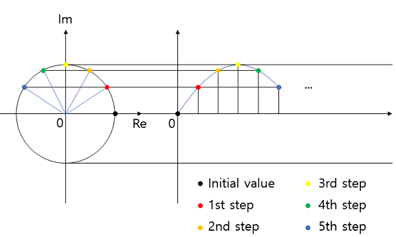
Figure 1: Example of complex number multiplication.
Challenges are:
- Signed large number multiplication in one clock cycle
- Rounding and Accuracy
- Transfer to a positive number (amplitude, offset)
- Calculating step size (Φ and complex numbers)
Verification of this procedure is done using FFT and looking at signal to noise ratio.
Since Xilinx DDS Sine Wizard gives up to 24 Bits resolution this realization targets 32 Bit.
- Precalculation of 32 to sine and cosine values for power of 2 fractions
sine(2 · π / 232 · 2i ) i=0..31 - Precalculation for a given frequency of step sine (Im) cosine (Re) by using for each bit the precalculated values
- Generating sine values
Applying the step to the current value
Accurate calculation for the next value 32*steps
sine_unit: sineX            -- Sine generator
   Port map (
       CLK => CLK,
       RST => xrst,
       step => step,            -- increment  in (31 downto 0) 32 bits
       amplitude=> amplitude,   -- signal amplitude in (31 downto 0) 32 bits
       offset => offset,        -- signal offset in (31 downto 0) 32 bits
       mysine => mysine         -- output waveform out (31 downto 0) 32 bits
   );
Sine Calculation example
fFPGA = 100 MHz
fsignal = 10 kHz
Number of points per cycle: Np = fFPGA/fsignal = 10000
step = 232 / Np = 429497
An FFT needs a power of 2 samples without windowing and an odd number of cycles to excercise as many levels of a data converter as possible
Choose NFFT:
NFFT (NBit) = 256 (8), 1024 (10), 16k (14), 1M (20), 16M (24), 1G (30)
Choose number of cycles:
Ncycle = 1, 11, 101, 1001, 100001
Calculate signal frequency:
Tsignal = NFFT / fFPGA / NCycle
fsignal = 1 / Tsignal = fFPGA * NCycle / NFFT
step = 232 / fFPGA * fsignal = 232 / fFPGA * fFPGA * Ncyle / NFFT = 232 * Ncyle / NFFT
NFFT = 1024
Ncycle = 17
fsignal = 100 MHz * 17 /1024 = 1.66 MHz
step = 71303168 = 04400000
| Number of cycles | frequency in kHz | Step |
| 3 | 1.40851 | 196608 = 3 * 64 * 1024 |
| 11 | 5.16452 | 720896 = 11 * 64 * 1024 |
| 101 | 47.419625 | 6619136 = 101 * 64 * 1024 |
+ Sine Simulation with JavaScript to verify VHDL
Oscilloscope
5 channel acquisition data are continously written into block memory. The current position and the number of samples is stored in position 2 and 3. These data are serially transmitted to the NodeJS server and then to the client (OSC).
The client sorts the data according to the bCount position (OSC1).
The trigger condition is searched in this data and data before and after the trigger point are extracted and displayed (OSC2).
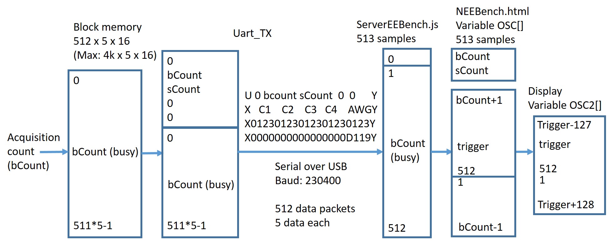
Figure: Acquisition
Details can be found in "Data Acquisition"
UART
Since the received data is directly stored in signal generator registers there is no need for a FIFO.
Implemented commands (uart_mem.vhd, getCmd: process):
"X": initialize
"S": sine signal, followed by 24-hex numbers: step, amplitude, offset each 32 bit
Example f = 1 kHz, amp = 1 V, offset = 1 V as shown in AWG1: S0000A7C526C9B26C26C9B26C
"T": triangle signal, followed by 20-hex numbers: start, stop, step (16-bit each), repeat (32 bit)
Example pulse f = 1 kHz, amp = 1 V, offset = 1 V as shown in AWG1: T00004D924D920000C350
Example triangle f = 1 kHz, amp = 1 V, offset = 1 V as shown in AWG1: T00004D8A001900000040
Example stair f = 1 kHz, amp = 1 V, offset = 1 V as shown in AWG1: T00004D8F0F8300002710
"U": start sending data: 514 chunks of block of data are sent: AWG, OSC1, OSC2, OSC3, OSC4; 16 bit each; 20 hex values
The first transmission has the current index stored. One extra transmission, because there can be an ongoing conversion at the current index.
"V": Connect switches to output
"O": Oscilloscope block size 16 bit and sampling rate 16 Bit (V_06)
Command: O00200000 : Block size x0020 = 512; timeBase 0000 8.32 us
The mapping of uart_mem to block memory not registers is done starting EEBench_V04.
The multiplexer for sine, triangle switch is also done in EEBench using signal waveselect.
Baud rate 19200, 52us per bit, sine command: 25(chars)*10(Bit)*52us(bit time) = 12.5 ms
Baud rate 230400, 4.34 us per bit, sine command: 25(chars)*10(Bit)*4.3 us(bit time) = 1.1 ms
Baud rate 230400, 512 points 22 hex values each T = 0.5 s
+ EEBench V02
- EEBench V04
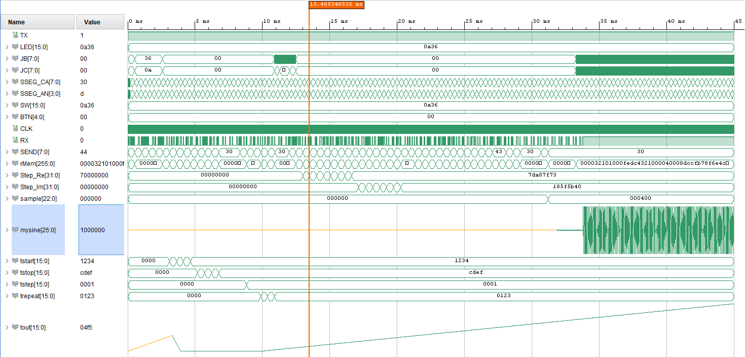
EEBench V04
The biggest change for V04 is the use of BlockRAM memory (myBuf) for data acquisition. After a "U" comman 514 x 5*4 Hex values are sent.
This is shown on the figure below.
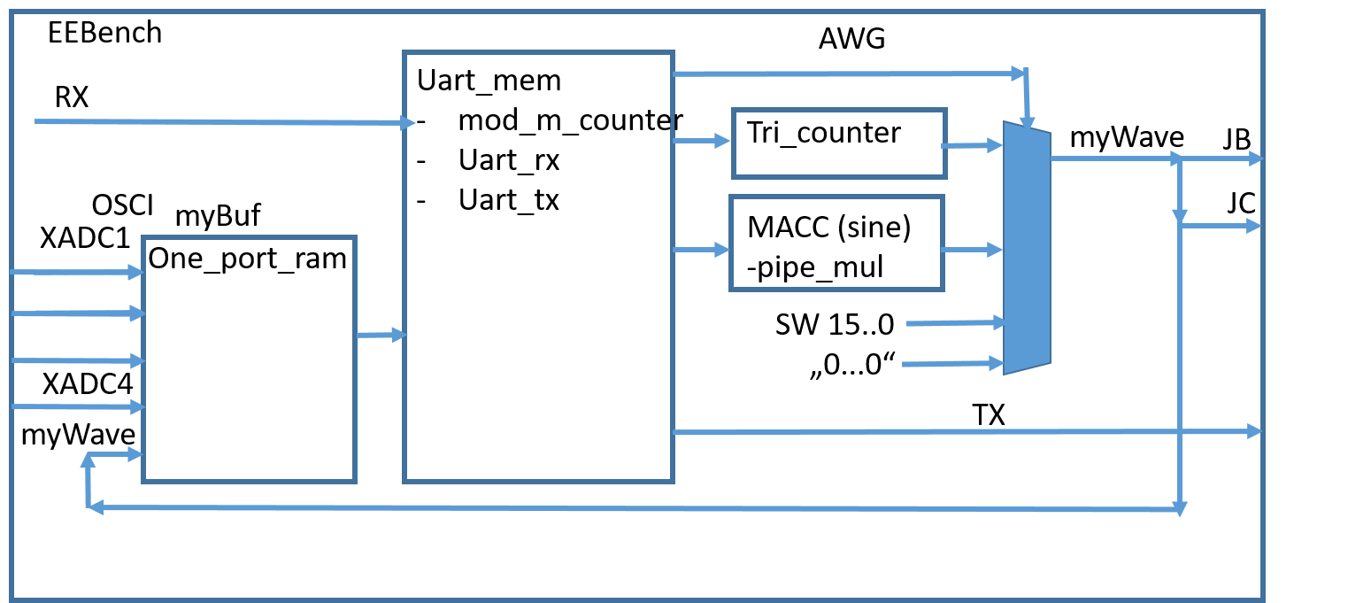
Figure: FPGA blocks for EEBench
Simulation shows:
- Receiving of serial command RX, decoded with SEND trace
- triangle and sine at mywave.
- Data transmission to PC TX and bCount(memory address)
data always zero since no data stored before
Figure: tb_EEBench.vhdl V04 simulation
Baud rate 230400, 4.34 us per bit, sine command: 25(chars)*10(Bit)*4.3 us(bit time) = 1.1 ms
+ Specification EEBench V05
EEBench V06
FPGA: Range of oscilloscope time base and buffer size should be extended.
Now the block RAM utilization is 2 out of 50 with 512 points. A factor of 16 8k points should be possible.
The transfer and sample block size should be user controlled.
So a UART command for change of sampling rate (16 Bit) and block size (16Bit) is implemented.
O<sampling><Block size>
Oxxxxxxxx
Update of NEEBench.js
Table: uart_mem: rxMem registers V06
| Input | memory address | Number of Bits | |
| rx_data_out | 0 | 8 | received command |
| a00000w1w0 | 8 | 8 | a '1' active '0' off w1w0: 01 sine, 10 triangle, 11 switches |
| Step | 16 | 32 | Sine step |
| amplitude | 48 | 32 | Sine amplitude |
| offset | 80 | 32 | Sine offset |
| (phase) | 112 | 32 | |
| (duty) | 144 | 32 | |
| tstart | 176 | 16 | triangle minimum start voltage |
| tstop | 192 | 16 | triangle maximum stop voltage |
| tstep | 208 | 16 | triangle voltage step |
| trepeat | 224 | 16 | number of samples per value |
| (phase) | 240 | 16 | |
| (duty) | 256 | 16 | |
| Block size | 272 | 16 | Oscilloscope block size (dataMax) |
| Time base | 288 | 16 | Oscilloscope time base (timeBase) |
- EEBench: rMem has already 512 Bits, initialization with 0 implemented
- uart_mem: UART receive set rMem: getCmd: process
when "01001111" => -- ASCII 49 O sine signal numD := "00001000"; -- 8 Hex numbers, (Step, amplitude, offset)x(8x4) rmAddress := to_unsigned(276,9); -- Start at index 276 (272 + 4) rx_mem(7 downto 0) <= rx_data_out; - Implement signals in EEBench:
dataMax for block size like variable NEEBench and timeBase
hook up rMem to dataMax and timeBase - For sampling a signal upSample is used
A process sampleRed is created to control sampling
-- sample rate reduction process --- time Base 000 upSample always 1 -- timebase 001 upSample 1-16-times-0-16-times -- timebase 010 upSample 1-16-times-0-32-times sampleRed: process(CLK, BTN(4), readyX) variable jCnt: integer; -- counter for reduction variable kCnt: integer; -- 16 samples begin if ( BTN(4) = '1') then -- asynchron reset with button 0 jCnt := 0; kCnt := 0; elsif (rising_edge(CLK) and (readyX = '1')) then kCnt := kCnt + 1; if (kCnt >= 8) then -- Clk divider 8 by kCnt kCnt := 0; jCnt := jCnt + 1; if (jCnt >= timeBase) then -- upSample short '1' long '0' upSample <= '1'; jCnt := 0; else upSample <= '0'; end if; end if; end if; end process; - TimeBase in NEEBench.html
- Introduce global variable timeBase
- Connect a serial command to change time base
timeBase > 200us/div timeBase = 1
timeBase = timePerDiv / 200E-6
timePerDiv is text input: id="baseVal" with unit value
Update of FPGA with 'Run' command and change in field (functions readCRX,comboBox)
Create function updateOSC for comboBox and readCRX
In updateOSC creat cmdO ="O00200000"; Block size x0020 = 512; timeBase 0 8.32 us
function confOsc() {
          var cmdO = "O";
		  // alert(document.getElementById("dataMax").value);
		  dataMax = parseInt(document.getElementById("dataMax").value); // 512: 0200
		  cmdO += decToHex(dataMax,4);           // Block size first
		  timeBase = Math.round(unitToValue(document.getElementById("baseVal").value)/200E-6);
		  cmdO += decToHex((timeBase + 1),4);   // Sampling next FPGA 0 and 1 same!
		  // update command field
		  document.getElementById("cmdTxt").value = cmdO;
		  sendCmdC();                           // send OSC configuration
}

window.addEventListener("load",confOsc());

function updateOSC(){
	   // update value field
       updateChanFields();
	   updatePlot();
       confOsc();
}
Attention interaction change during data acquistion? Probably not, only one bad display
Adjusted var timestep in function socket.on('newData', function (data) {
- Verification of timeBase FPGA code and NEEBench.html
Compilation FPGA, html and js correct during loading
Operation: timeBase 0,1 give same maximum sample rate for FPGA -> fix NEEBench
Operation: 2 ms/div x axis not fully filled? Sample rate too high time Base too low fixed with the following code
timeBase = Math.round(unitToValue(document.getElementById("baseVal").value)/200E-6); cmdO += decToHex((timeBase + 1),4) // Sampling FPGA 0 and 1 sre the same - Block size NEEBench: already global variable dataMax present
Tab configuration field 'Sampling memory size' with selection 1,2,4,8,16,512,1024,2048,4096,8182
Read field before sending command
Use field value during receiving data
var timeSampling = unitToValue(document.getElementById("timeSampling").value); var timestep = timeSampling * (timeBase + 1); // XADC 10ns * 8 * 104 cycles conversion - Block size FPGA EEBench
- Increase memory size of structure:
one_port_ram.vhdl defines blockRAM
Instance: myBuf: One_port_ram with signal addr (addrUART, addrGen)
uart_mem aBuf, tma, tmAddress - Increase acquistion
- Increase uart transfer FPGA, ServerEEBench.js, NEEBench.js
- Debugging of block size and sample rate with AWG as reference and FFT gave 96 dB equivalent to ENOB = 16 Bit
- Open: Challenge of acquisition for large Blocks and large sample times
- At the moment AWG and ADC data is stored all the time in memory.
When a data request is received sampling stops and the data is transfered
as block to the client. This takes 0.5s for 512 data and current baud rate.
The client waits until all block data is received
and updates the chart.
During Run operation every 1 second an Intervall function tries to get new data.
For large blocks or large acquisition times update is very slow.
Solution: There should be a plot every n received data?!
Solution: Large times should have small block sizes and acquisition continues?
- Open:
When to switch from block transfer to individual transfer?
Should the block size be automatically adjusted?
Update setInterval adjustment?
User interface
+ Arbitrary Waveform Generator
- NodeJS
Starting point is copying of the HTML and Javascript sources to C:\temp\NodeEEBench
The following files are important:
NodeEEBench.bat this starts ServerEEBench.js
ServerEEBench.js the nodeJS server file
In the subdirectory Projekte the file Signalgenerator_221111.html is located.
An example of nodeJS communication is done in Webeditor.
The latest version of serial port on windows requires the following commands:
   var SerialPort = require('serialport').SerialPort;

   SerialPort.list().then(  // List available serial ports
       ports => ports.forEach(console.log),
       err => console.error(err)
    );

    var serialPort = new SerialPort({
      path: "COM22",        // port name
	  baudRate: 230400      // Baud rate befor 19200, 52 us per bit
    });
The io.on subroutine detects user connection and logs it on the console.Then the socket event of a cmd from the client is implemented.
The most important feature is to detect the block size for sending data.
The serialPort.on 'data' subroutine collects data from the serial port and emits it to the client.
    io.on('connection', function(socket){
		var con = true;                             // connection still valid?
        console.log('An user is connected')

        // get data from connected device via serial port
		var dataBuf="";

         socket.on('cmd', function(data){     // get client event
        	var cmdName = data.value;        // cmd passed from client
        	console.log('cmd: ' + cmdName);
			if (cmdName[0] == "X"){
               dataBuf = "";
			}
    	    if (cmdName[0] == "O"){   // oscilloscope block size next 4 hex values
               dataMax = hexToDec(cmdName.substring(1,5));
			   console.log('Block size: ' + dataMax + "x" + cmdName.substring(1,5) + "x");
			}
    	    serialPort.write(cmdName);           // hex(cmdName)
			// insert server action commands
			// var data= "Test Data:" + cmdName;
    		// socket.emit('newData',{value: data });  // send data to client
        });

	    serialPort.on('data',
		  function (data) {
		    // get buffered data and parse it to an utf-8 string
			var data1 = data.toString('utf-8');
			dataBuf += data1;
			// you could for example, send this data now to the the client via socket.io
			// io.emit('emit_data', data);
			if ((dataBuf.length >= 22 * dataMax ) && (con)) {   // complete set
			 console.log(dataBuf.length/22 + "," + dataBuf.length + "," + dataBuf.substring(0,50));     // dataBuf
		     socket.emit('newData',{value: dataBuf});  // send data to client
			 dataBuf = "";
			};
 		 } );

        socket.on('disconnect', function(data){
    	    console.log('An user is disconnected');
			con = false;
        });
    });
+ Oscilloscope
Oscilloscope User interface
Figure: Oscilloscope interface V05
The figure shows the oscilloscope interface with the run button at the top.
Acquisition options are shown with xy-axis selection operational for version 5.
A trigger source, condition and level can be chosen.
On the left are the axis control with offset (position) and range (base).
Below are 2 buttons to load example data and look at the data with save.
The curves are color coded displayed and typica measurement values are displayed at right column.
Cursors and math functions are still missing.
+ ComboBox
Run Button
The icon changes from run to stop.Run emits a serial "U" command from client to server (function oOp('Run')) and starts a (handlerOsc = setInterval(runOsc,1000);) continues sampling every second. busyOsc = 1; and oState = "Run"; is set
Stop emits ..(function oOp('Stop')) and sets oState = "Stop";
Acquisition
Version 5:A block of 512 data points is acquired and searched for a trigger point and 256 data points are selected for display.
5 16 bit values as 4 hex digits each are sent with a start and stop character.
Here is an example for 2 samples 5 channels each.
U4710FF0F471000000000YX0000000000000000D119Y
A new block starts with an "U" and each data value is limited by an X and Y.
Trigger
Trigger implementation
Measurements
Measurement data are generated with function chanStats().
For each channel the data points are searched for minimum and maximum and average is calulated.
     var min = dataOSC2[i*dataMax/2];
     var max = min;
	 var avg = min;
     for (var i1 = 1; i1 < dataMax/2; i1++) {
       var point = dataOSC2[i*dataMax/2 + i1];
	   if ( point < min) min = point;
	   if ( point > max) max = point;
	   avg = avg + point;
     }
	 channels[i].min = min;
	 channels[i].max = max;
 	 avg = avg/dataMax*2;
	 channels[i].average = avg;
     channels[i].amplitude = (max - min)/2;
Everything is stored in the object array channels.Average value is used for period and frequency.
Each crossing of the average value of the curve is collected.
	 // period and frequency
	 var t = new Array;
	 for (var i1 = 1; i1 < dataMax/2; i1++) {
       var point1 = dataOSC2[i*dataMax/2 + i1];
	   var point2 = dataOSC2[i*dataMax/2 + i1 - 1];
	   var point3 = point1;
	   if (point1 > point2) { point1 = point2; point2 = point3; }
       if ((point1 <= avg) && (point2 >= avg)) {
	      t.push(i1);
       }
     }
Finally the differnece between 2 crossings and the average of these numbers is used for frequency and period.
	 // Differences between t(i) half period
	 var tx = new Array;
	 for (var i1 = 1; i1 < t.length; i1++) {
	    tx.push(t[i1]-t[i1-1]);
	 }
	 var periodAvg = 0;
	 for (var i1 = 1; i1 < tx.length; i1++) {
	    periodAvg += (t[i1]-t[i1-1]);
	 }
	 periodAvg = periodAvg / (tx.length-1) * (dataOSC2[1] - dataOSC2[0]) * 2;
	 channels[i].period = periodAvg;
	 channels[i].frequency = 1/periodAvg;
The displayed values can be easily selected and copied.FFT
Figure: FFT interface V05
The figure shows the user interface for the FFT. The Run button activates and runs the FFT once. 256 data points at 8.32 us acquisition give a minimum frequency of 4.6 Hz and a maximum frequency of 60 kHz.
Data was generated internally with the function generateData().
The y values of the channels were scaled by C2 256 (8*6 = 48 dB), C3 4096 (12*6 = 72) and C4 2M (21*6 = 126 dB).
For C3 the largest peaks are listed (choose via channel select list).
For C3 at 2.4 kHz the signal has -3.01 dB and total noise is -76.7 dB as expected.
C1 has 280 dB signal noise ratio equivalent to 280/6 = 46 Bits.
The y axis has a fixed range implemented.
Ideal sine curve calculation can give more than 32 bits -192 dB.
Typical user cases have to be investigated to improve the y-scaling.
Details can be found in FFT Implementation
Histogram
Figure: Histogram interface V06
- Run button (function hOp(cmd))
- Combo box number of bins (var nBin)
- Function generate histogram (var histo = new Array();)
- Chart: canvas id="histoChart"
16 Bit R2R DAC as AWG1
The 16 Bit R2R DAC has a voltage range from 0..3.3V. To study error correction 100k and 220k resistors were used. In a first step the DAC is tested with the 12-Bit ADC with a range from 0..1 V of the FPGA.
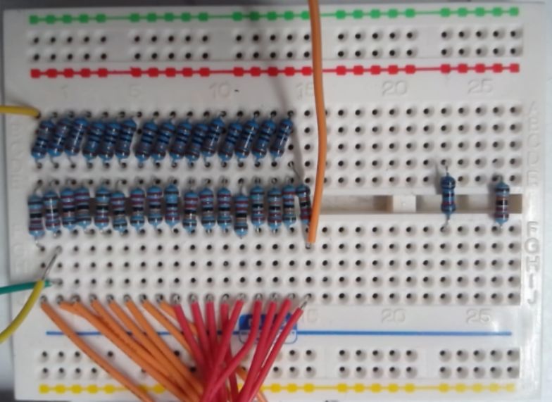
Figure: 16 Bit R2R DAC with R=100kOhm and 2R=200kOhm
Due to the range of the ADC and no circuit between the DAC and ADC only 12-Bit can be tested. The goal is to measure a 12-Bit resolution between 0..1 V for the DAC.
First full range and mid range settling times are measured. This is compared to the frequency behaviour.
Slow output rate and high resolution with a buffer of 4k samples require multiple measurements for ramp and sine tests.
Test control needs to be implemented in software.
Noise can be measured with FFT and a code histogram at fixed output levels.
For error correction a lookup table and step compensation can be used.
A lookup table is generated using the inverse ramp test values. It can happen that more than one output code will produce the desired output voltage. The code which gives the easiest corrrection factor is taken.
Step compensation can be determined by looking at the offset needed for each code to get the correct output value.
For codes above certain values an offest (step size could also be changed?) is added. A comparison can be easily implemented in the FPGA for a high (16..256) number of values.
Lookup tables up to 8k can be implemented in the FPGA block memory.
Error correction has to be implemented.
Basic questions for DAC investigation:
- What is the code resolution of the XADC output?
There seems to be a 16 Bit output. - What is the signal bandwidth of the DAC?
A signal frequency of 1.4 kHz and 5.1 kHz give a signal level of -10 dB
A signal frequency of 47.4 kHz gives -15 dB
- How can the bandwidth be improved?
Can prescaling or digital filtering help? - How is it possible to construct a LUT with noisy data?
- What is the SNR improvement using a LUT?
- It is necessary to use high number of FFT samples?
- What is the influence of windowing, number of cycles on SNR/ENOB harmonics?
Settling time (Pulse)
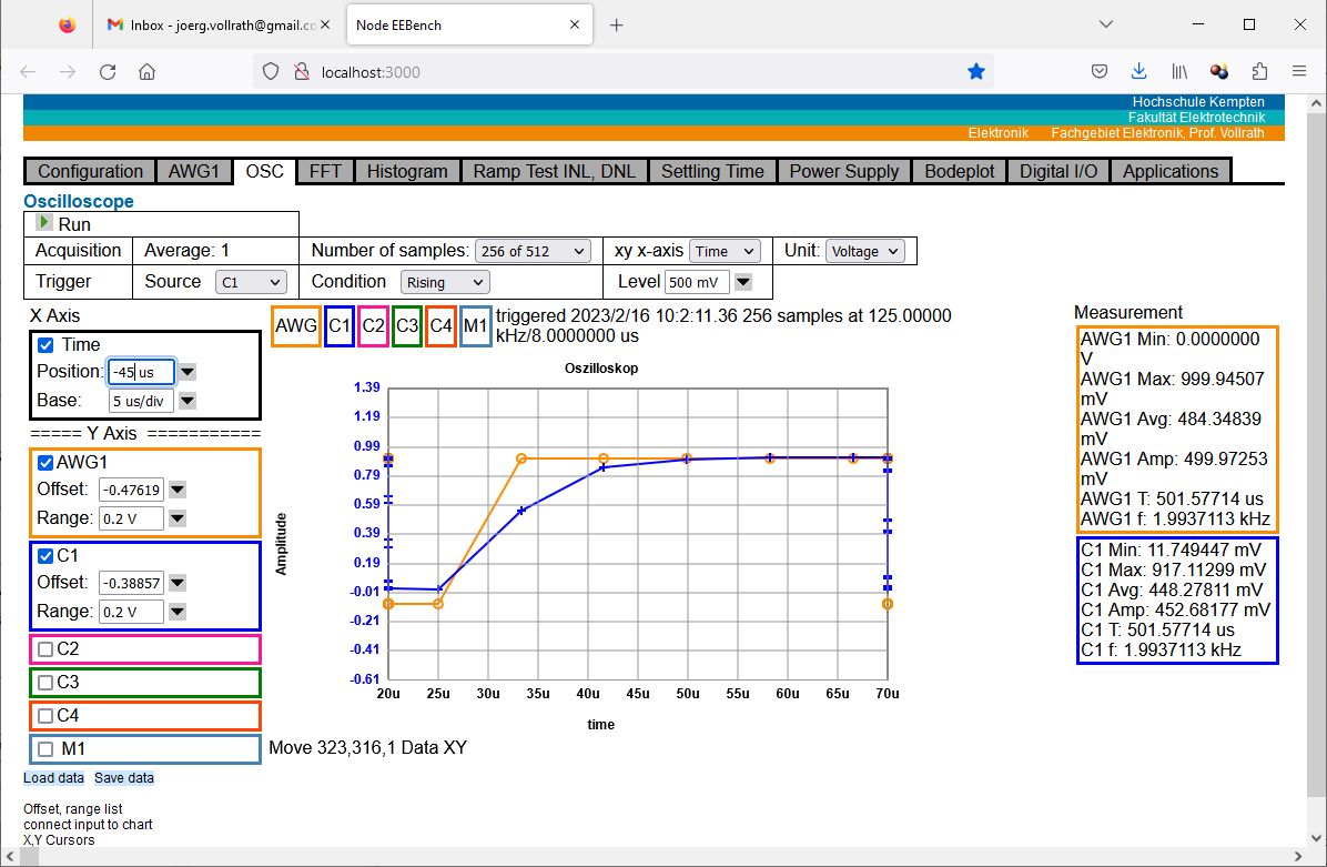
Figure: Settling time of rising edge oscilloscope data
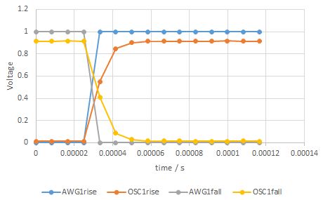
Figure: Settling time data in Excel
After 83 us the change in output value is less than 0.5 mV which relates to 1/2000 of full range of 1 V and a bandwidth of 12 kHz.
A maximum slew rate of S = 0.5 V / 8.3 us = 60 V / ms can be seen.
Further questions:
Reduction of signal level of FFT at which frequency?
Noise level
Next the noise level is investigated for a DC signal.
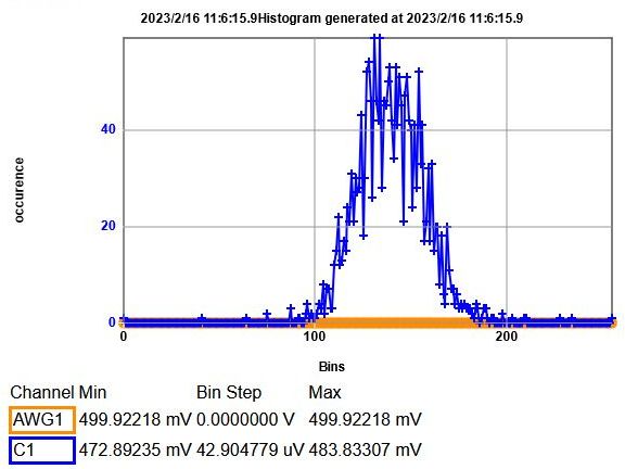
Figure: 0.5 V DC Histogram with 2048 samples
11 mV voltage level variation of noise can be seen.
With a range of Vmax = 1 V, LSB = Δ = 11 mV step size gives 1 V / 11 mV roughly 27 = 128 levels, ENOB = 7 bits and SNR = 42 dB.
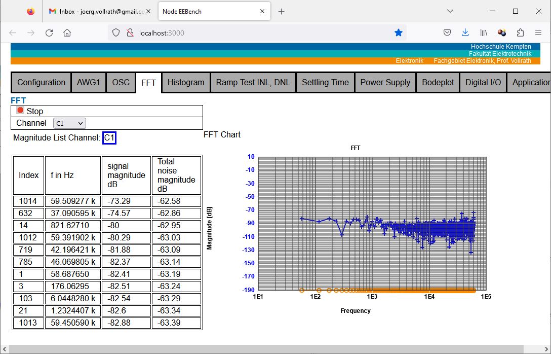
Figure: 0.5 V DC FFT with 2048 samples
The FFT gives a total noise level of -62 dB. This has to be compared to a maximum possible signal level of -9 dB giving an ENOB = (-9 dB - (-62 dB))/6 dB = 9 Bit.
Since the ADC has 12 Bit according to the data sheet, it is 3 bits less than expected.
INL, DNL (triangle)
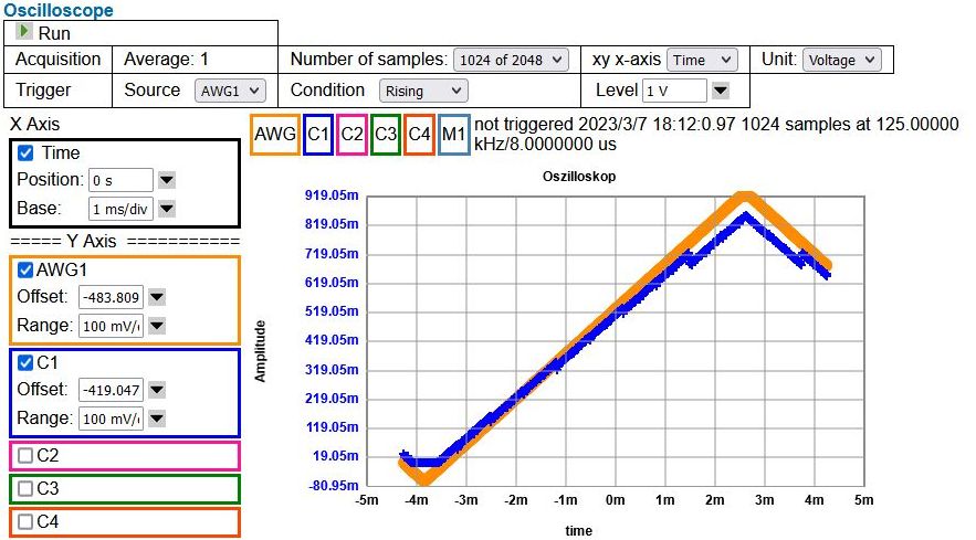
Figure: Ramp measurement
Applying a ramp signal from 0V to 1 V gives a code range from 8 to 18948 for AWG1 and 0 to 55995 for OSC1.
The expected maximum code for AWG is 1 V / 3.3 V * 64 * 1024 = 19549
It is interesting that the 12 Bit ADC gives a 16 Bit code (XADC, VHDL, JavaScript?).
The blue curve shows non idealities due to the bad resistance ration of 100k/220k.
Code range 0..22k
1 Measurement gives a maximum of 4k/8k points.
To get an optimum match at least 4..8 measurements are needed.
To match the measurements the measurements should overlap by half(?) the range.
The number of measurements is increased if noise has to be reduced with averaging.
FFT and SNR (sine)
The FFT prcoess is described in detail in 'FFT Implementation' showing a source synchronous odd integer number of periods is necessary for accurate high precision measurements. Windowing decreases the signal level and distributes the signal over many bins (next figure). The best window in this simulation study is the Nutall window.
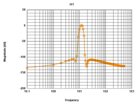
Figure: Windowing with Nutall window a non integer number of periods for FFT (FFT playground)
A 1 V DAC range is covered with a sine signal with 0.5 V offset and 0.5 V amplitude. 1 V rms voltage gives 0 dB. Therefore 0.5 V amplitude gives a factor of 0.5 * \( \sqrt{2} \) giving -9 dB.
Table: Frequencies and UART commands for FFT testing
| Number of cycles | frequency | step size | UART command |
| 3 | 1.40851 kHz | 196608 = 3*64*1024 | S000300001364D9361364D936 |
| 11 | 5.16452 kHz | 720896 = 11* 64 *1024 | S000B00001364D9361364D936 |
| 101 | 47.419625 kHz | 6619136 = 101 * 64 * 1024 | S006500001364D9361364D936 |
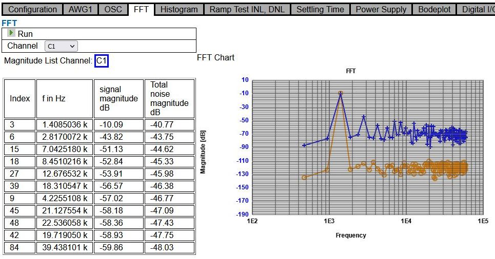
Figure: 256 samples FFT and SNR for a 3 cycle sine wave of 16 BIt R2R DAC
The figure shows the typical 256 sample FFT of a sine signal of 3 periods. The blue curve is the DAC output signal, the orange curve is the digital signal of the sine generator (AWG). The table on the left shows frequencies and magnitudes sorted by magnitude.
The peak level of -10.09 dB for the 1.4 kHz sine signal can be seen. The total noise is listed as -40.77 dB. This gives an ENOB = (-10.09 dB - (-40.77 dB) ) / 6 = 5 Bits
The next lines show the harmonics and the remaining total noise level without the harmonics.
The first harmonic is at -43.82 dB below the total noise level and the total noise level is reduced to -43.75 dB without the harmonics.
The harmonics stem from non linearities, INL, DNL errors. Calibrating the DAC could eliminate harmonics and increase ENOB. Increasing the signal to noise level by eliminating the first 5 highest harmonics would lead to a gain of one more Bit.
Figure: 256 samples FFT and SNR for a 101 cycle sine wave of 16 BIt R2R DAC
To study bandwidth limits a higher frequency of 47 kHz was selected next. It can be seen that the signal magnitude decreased to -10.1 dB.
Simulation of 6 Bit R2R DAC Calibration
Unfortunately a calibration of the 16 Bit R2R DAC could not be done in the given time frame. Only a preliminary simulation with LTSPICE was done with a 6 Bit R2R DAC.
Figure: 6 Bit R2R DAC test circuit
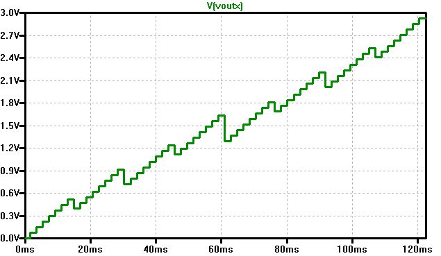
Figure: R2R 3 bit error ramp simulation
LTSPICE: 6Bit_R2R_DAC_Test.asc
The minimum voltage is 0 V and the maximum 2.92 V with multiple slope reversals at the 3 most significant bits (MSBs).
The data was transfered to Excel and a LUT was realized with the Excel function vlookup(Sverweis) with 32 codes.
Starting from vlookup a manual fit was attempted and could not resolve INL and DNL for 2 codes (1, 30) at the beginning and end.
Reducing the range could make it possible to loose only 1 Bit.
The range is reduced with a reduced number of bits: 63 (6 Bit), 31 * 2 = 62 (5 Bit), 15 * 4 = 60
There seems to be no easy calculation from input code to adjusted DAC code (compare orange and blue line).
INL and DNL stay barely below 0.5 (right axis for grey and yellow curve).
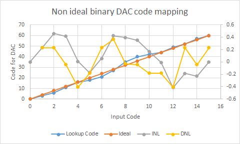
Figure: Mapping 4 Bit input code to 6 Bit output code
Table: INL and DNL after calibration with lookup code
| yCode | Lookup Code | Ideal | INL | DNL |
| 0 | 0 | 0 | 0 | |
| 1 | 3 | 4 | 0.2297571 | 0.2297571 |
| 2 | 6 | 8 | 0.4595142 | 0.2297571 |
| 3 | 11 | 12 | 0.41599184 | -0.04352236 |
| 4 | 16 | 16 | 0.00809729 | -0.40789455 |
| 5 | 18 | 20 | -0.17206464 | -0.18016193 |
| 6 | 21 | 24 | 0.05769246 | 0.2297571 |
| 7 | 27 | 28 | 0.4240888 | 0.36639634 |
| 8 | 35 | 32 | 0.39574927 | -0.02833953 |
| 9 | 40 | 36 | 0.35222657 | -0.0435227 |
| 10 | 42 | 40 | 0.17206464 | -0.18016193 |
| 11 | 44 | 44 | -0.00809729 | -0.18016193 |
| 12 | 49 | 48 | -0.41599217 | -0.40789488 |
| 13 | 52 | 52 | -0.18623441 | 0.22975776 |
| 14 | 57 | 56 | -0.22975644 | -0.04352203 |
| 15 | 60 | 60 | 0 | 0.22975644 |
Interesting is to look at the code difference between lookup code and ideal code.
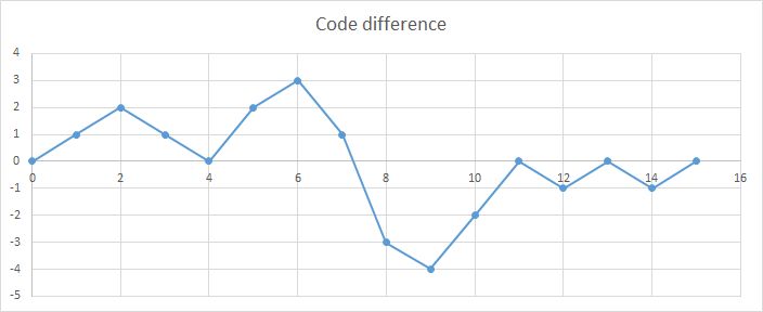
Figure: Code difference of lookup and ideal
User circuits
Some ideas for user circuits which can be tested implementing additional functions in software and hardware are presented here.
A simple RC circuit.
AWG1 signal is externally applied to an RCL circuit and the output voltage is measured with OSC.
Instead of an RC circuit a switched capacitor Cswitch,CL circuit can be used. The switches should be digitally controlled. Cswitch should match the R and the output should match the first result.
Cswitch = 1/R/fPGA
Third option would be a digitally processed digital AWG1 signal which is displayed after signal processing in the OSC window or fed to AWG2 for output and can be measured with OSC.
Voutn+1 = Voutn + (Vinn-Voutn)/R/fCLK/C
Voutn+1 = (Vinn + Voutn * ( R * fCLK *C - 1)) * 1/R/fCLK/C
How does the schematic symbol look like?.
These 3 design options can be compared.
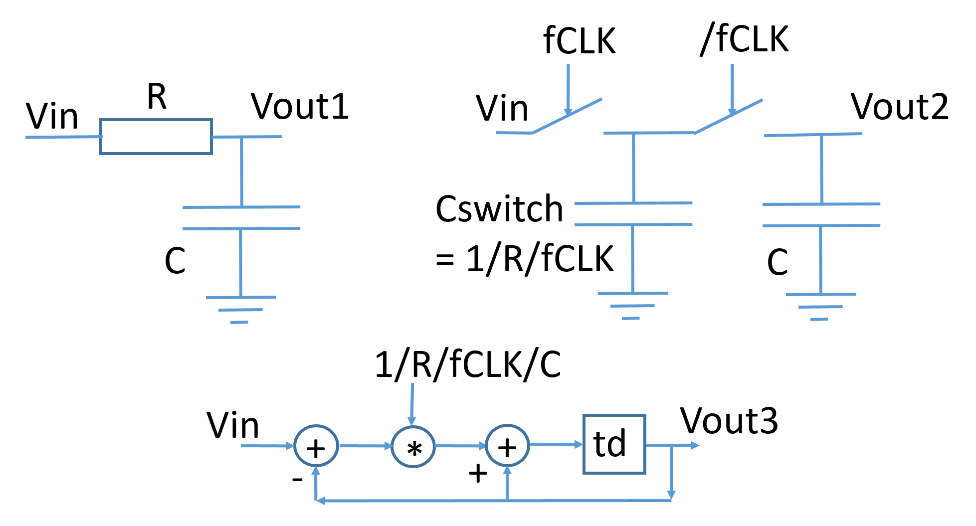
Figure: RC Circuit realizations (td=1/fCLK)
A DAC/ADC error correction
The internal digital sine signal is fed to a lookup table or equation and then diplayed (OSC) and passed to the external DAC under test.
The OSC input signal is digitally processed via equation or lookup table and the resulting signal displayed or processed for DNL, INL and SNR.
Filters, control loops, ...
Paralell, seriell conversion
Taking the AWG sine code and converting it to a serial DAC code.
Taking serial gray code output of a pipeline ADC and converting it to binary numbers.
- Proposal for EEBench hardware
At this point, having a working oscilloscope and R2R DAC, a review of hardware concepts in available hardware is done to be able to realize a low cost EEBench.
The main hardware components are microprocessor or FPGA, memory, ADC, DAC, analog switches, operational amplifiers and power supplies.
Components are selected based on the public available resources from (Red Pitaya, Digilent, ADALM) and prices are looked up at Digikey.
- FPGA: XC7Z007S-1CLG400 61.- (ZinQ), XC7A35T-1CPG236C 48.71 (CORA Z7), XC7S25-1CSGA225C 38.70 (BASYS3, CMOD S7)
- Memory: 512 MBit SRAM (IS61WV204816BLL-10TLI) 25.- (CMOD A7)
Memory: 16 MBit SDRAM 2.65, 8GBit 512Mx16 10..30.-, 1GBit 64Mx16 5.- - ADC: AD9648 Dual 14-bit, 105MS/s, 90.- (Analog Discovery)
- DAC: AD5643 15.- Dual 14-Bit Interface: 50 MHz (Analog Discovery) general
DAC: AD9717 30.- 14Bit 125MS/s, AWG - Analog switch: ADG612 6.50 (Analog Discovery)
- Amplifier: ADA4940 6.-, AD8066 7.5, ADA4051-2 5.- (Analog Discovery)
- Power:
Can a ADC video encoder circuit be used as oscilloscope?
Video CODECS: ADV7281 20.-;
A proposal for needed input and output for EEBench hardware and needed physical dimensions is done.
32 or 40 digital IO pins are needed to be able to realize 2 16 Bit DACs and some SPI or I2C interfaces.
There should be 2 arbitary waveform generators, 2 reference voltages Vref, a positive VP+ and negative VP- higher power supply, 3V and 5V power supply and a maximum of 8 channels for an oscilloscope.
Resulting in a total of 56 pins plus gnd connections (8)
EEBench Hardware (56+gnd): 32(40) digital IO, 2 x 16 Bit DAC(AWG) + SPI/I2C Interface, 2 AWG, 2 Vref, VP+, VP-, 3V3VCC, 5VDD 8 Chan OSC
This hardware could be physically realized in a small breadboard size of 59 x 80 mm2 which gives up to 32 pins each at the long sides of the board.
- EEBench Hardware: Breadboard 59x80mm2 29+ pins long: 32 pins gnd,VP+(-),Vref1(2),AWG1(2),gnd,OSC1,2,3,4(5..7),gnd,5(3)V,20 IO,gnd
Breadboard power supply
Having a working ADC and DAC the next step would be to implement a power supply. The power supply is needed for IV characterization and to supply additional operational amplifiers (VP+, VP-) or logic circuits (3.3 V 5 V)with power.
There should be different versions.
- The simplest solution is just USB connector to breadboard.
- The next would be USB connector and negative voltage -Vin generator
- For battery operation 1..1.5V it would be nice to have 2 * Vin and -Vin
- Voltage control with DAC and PMOD/USB interface would be nice to have for range 2 * Vin and -Vin
- Prefered is a charge pump up to 1.5A
- Prefered is an adjustable current limit
Power supply VPP+ VPP- AWG1, AWG2
3V3 VPP+ VPP-
Low cost power supply
A power supply needs a serial controlled DAC to adjust the output voltage. Amplifiers are needed as output buffers.
Again present hardware is studied.
Charge Pump: LM27762EVM 0.25A
OpAmp: 2 x AD8542 (DAC->regulator/AWG)
4 chan DAC I2C: AD5645R (internal reference) 12.-
4 chan DAC I2C 12 Bit MCP4728 Adafruit 4470 8.-
For DAC control I2C interface
SCL Pin 1
SDA Pin 2
ADDR1, ADDR2 jumper GND, VDD, Pin3,4
USB Interface can be realized with ESP32 connected to VCC, GND, SDA, SCL.
Schematic is based on Analog Discovery 2 and LM27762EVM.
A first proposal for the physical outline of a power supply board is shown below:
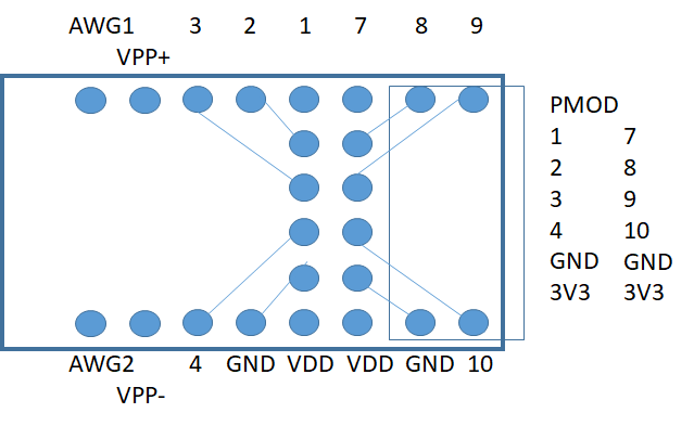
Figure: Board pins for PCB
Missing is the output driver (Opammp, non inverting) for AWG1 and 2 to generate from 0..3 V 3 to VOUT+ .. VOUT-. (Is this a good concept?)
The following figure shows a circuit concept from the Analog Discovery 2 and the evaluation board LM27762EVM.
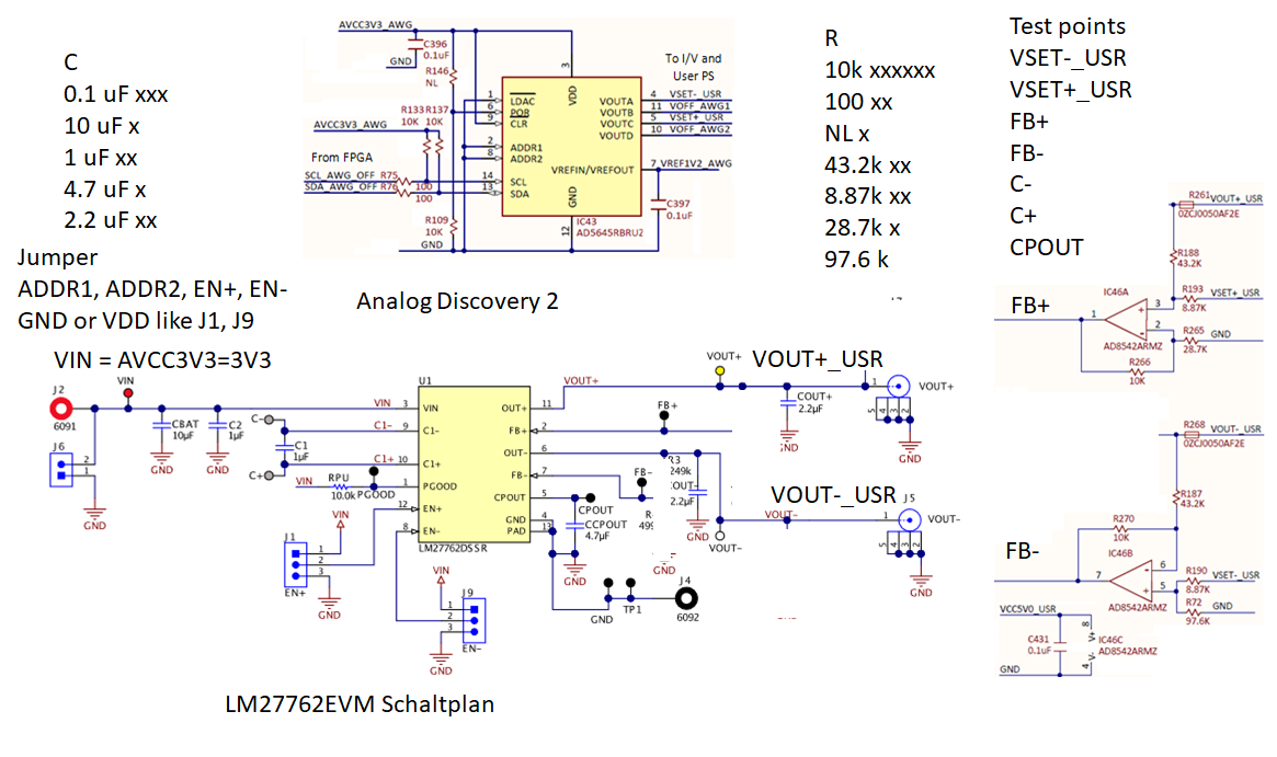
Figure: Power schematic
List of parts:
Charge pump: LM27762DSSR (2.-) (LM27762EVM 50.-) Package: WSON-12 250 mA
Operational amplifier: AD8542ARMZ
C: 0.1 uF xxx, 10 uF x, 1 uF xx, 4.7 uF x, 2.2 uF xx
R: 10k xxxxxx, 100 xx, NL x, 43.2k xx, 8.87k xx, 28.7k x, 97.6 k
Jumper: 3 pins/holes for: ADDR1, ADDR2, EN+, EN- (GND or VDD like J1, J9)
PMOD connector female
Breadboard connector 8 pins for top, bottom ( with female connector like Arduino?)
A charge pump has only capacitors no inductance and would be easy to implement. An ideal charge pump specification would be output voltage 2Vin, -Vin, output current 1 A, package DIP for breadboard or TSOP for soldering and price less than 2.-
Review Charge pumps 2Vin,- Vin Digikey:
MAX680 (5.-) DIP 10mA, LTC3265 (23.-) TSOP 100 mA (Evaluation board DC2235A 105.-)
Since a charge pump for 2 Vin and -Vin can be realized with 2 Inverters (phi, phib) and 2 NFETPFET pairs per voltage. A research was done to realize the charge pump with NFET, PFET pairs and study if more than 250 mA output current is possible.
Charge pump
Figure: Voltage doubling or inverting charge pump
The figure shows the charge pump circuit with 2 NFETPFET pairs, 4 capacitances and a load resistor R1. The control signals phi1 and phi2 should be also generated by low resistance NFETPFET pairs. Detailed measurements and simulations are documented in Breadboard charge pump circuit
The following parts were used:
CD4007 (0.6.-)
FDG6320C (1.-), 50 Ohm measured output resistance,at Vin=3.3 V, Vout = -2.2 V, RL = 100 Ohm, 22 mA output current
MCMNP2065A-TP (0.4.-), RDSon = 25 mOhm,
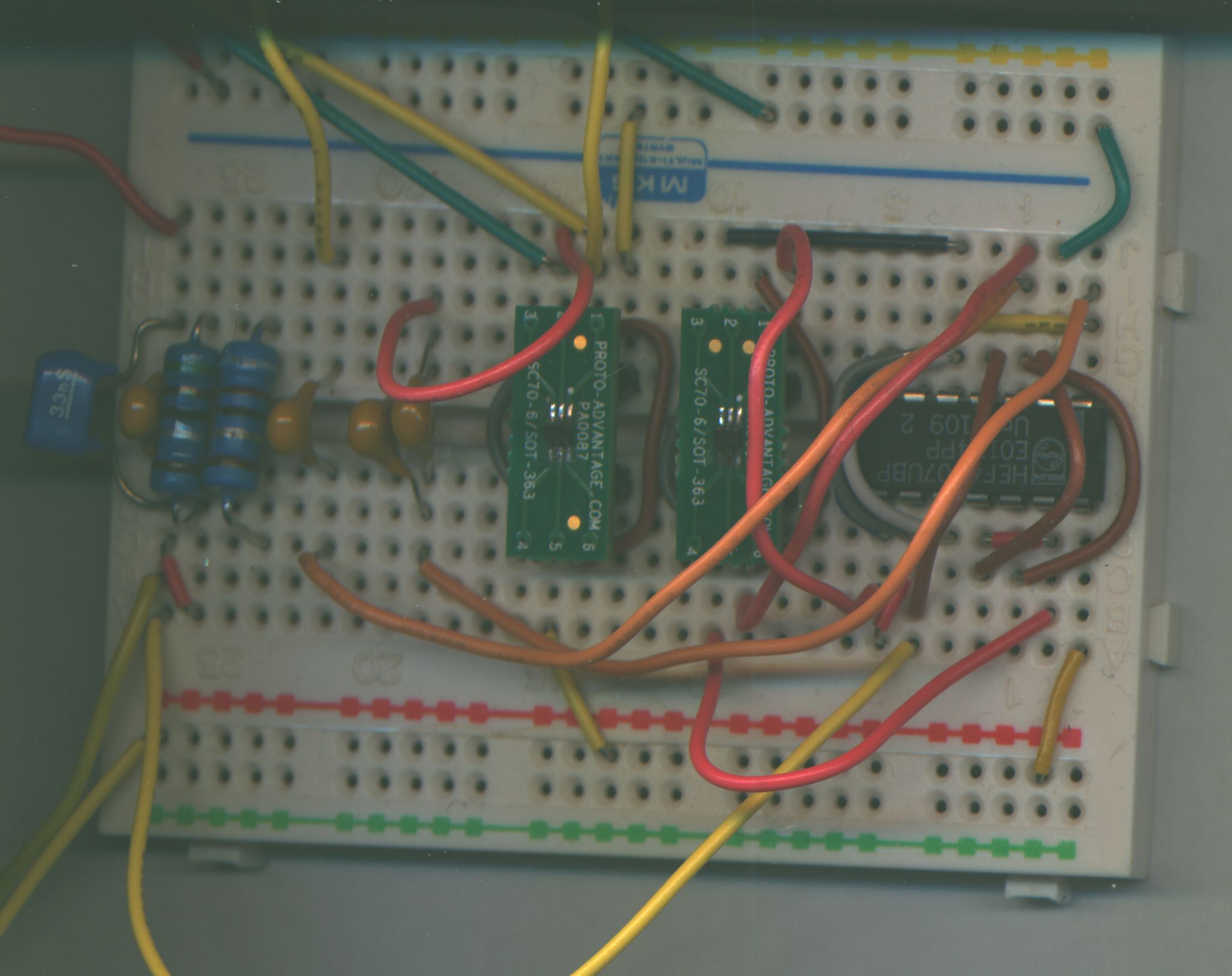
Figure: Charge pump on a breadboard
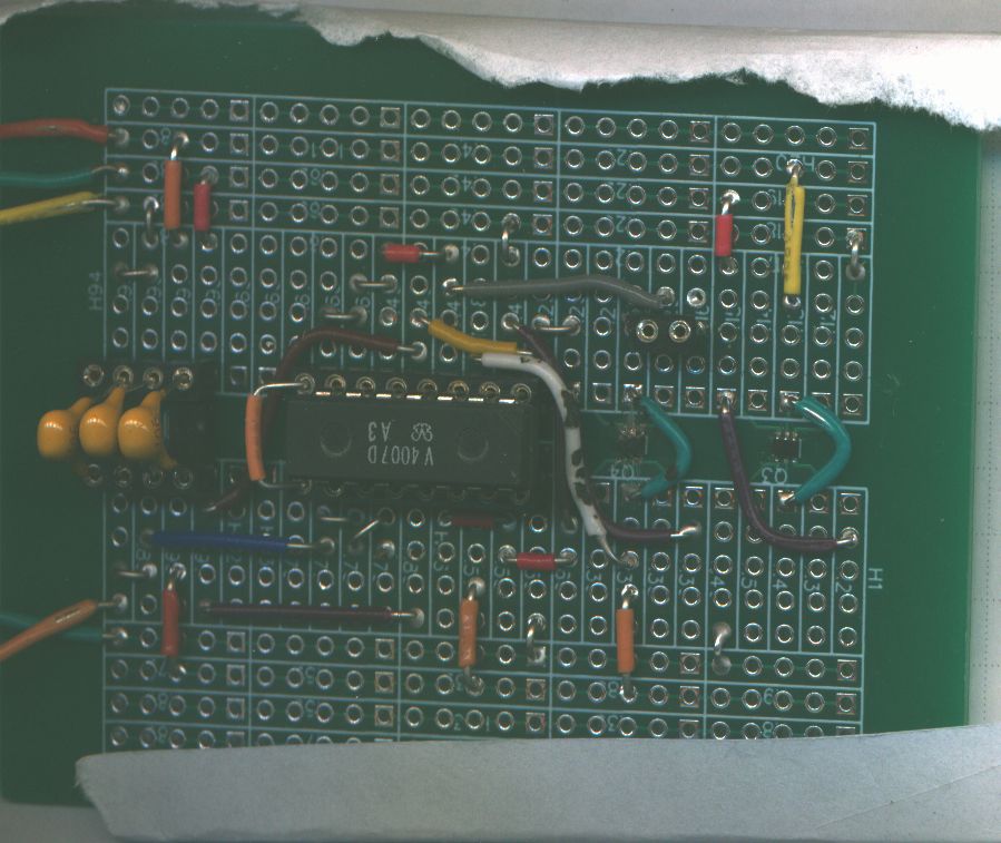
Figure: Charge pump on a PCB
CD4007 at VDD=Vin=3V with C = 10uF (106) gives a maximum of 30..200uA current with a ripple Vout < 20 mV starting with f=1 kHz.
FDG6320C shows a current up to 3mA at 1kOhm. At higher currents ringing occurs. Starting with 500kHz ringing is not that bad up to 1 MHz. f = 1 MHz; RL = 100 Ohm; gives Voutavg = -1.7V; dV = 0.6V; IVP+ = 23 mA;
MCNP2065 was not measured yet.
At the moment the LM27762 seems to be the best option. The price for the evaluation module is very steep and the size is not convenient. A PCB with PMOD connectors should be designed.
As a research project a charge pump with different NFETPFET transistors giving 2Vin/-Vin is still very interesting. A power operational amplifier can be used as output driver to make the output voltage variable.
Summary
A good survey of available ADC and DAC components and available measurement systems was compiled as starting point.
Limitations in the open source design and high costs of these systems led to the development of an FPGA based open source hardware and software platform.
The FPGA runs at 100 MHz, 4 ADC channels with acquisition rates up to 1 MSs and a 16 Bit R2R DAC was realized. VHDL code for the FPGA to realize a 16 bit arbitrary waveform generator, a 4 channel 16 bit oscilloscope with 8k sample memory and UART control was created. A nodeJS server provided a web interface to control the FPGA via the USB serial interface using a browser window. A GUI for the general configuration, for the arbitrary waveform generator with waveform control, frequency, amplitude and offset, the oscilloscope, fft and histogram was created.
The oscilloscope allows trigger selection, sample memory configuration, data export, channel selection and display of waveform characteristics.
A nice HTML user interface, code display of ADC and DAC values and open source hardware and software design provide a lot of opportunities for further activities.
Using a lot of libraries and hardware experience to build on, accelerated the development process. During the limited research time a basic system was realized, but there are still many open and new topics for improvement.
New challenges, which were not anticipated, came up during realization:
- Adjusting sample rate, buffer size and x-axis time per division for a good user experience
- Accuracy of control values for frequency, amplitude and offset for arbitrary waveform generator and oscilloscope. Hih accuracy and number of digits caused bad display of waveforms and input fields, but was needed to realize exact frequencies and voltage ranges for data converters.
- Displaying the original AWG signal in the oscilloscope view allows better comparison of source and sampled signal
- Normally an oscilloscope has the same sampling rate for all channels. Using a sampling scheme with a multiplexer the number of ADC components and the cost can be lowered and a sampling scheme like C1,C2,C1,C3,C1,C2,C1,C4 could give C1 as high speed channel and C2,C3,C4 as lower speed channels optimizing the utilization of the ADC.
- Having direct control of the commands send to control the FPGA allows easy implementation of new features
- Displaying ADC and DAC codes instead of calculated voltages allows easier analysis of data converter properties
- Arbitrary waveform generators allow to load a waveform, but not a lookup table which can be applied to different waveforms
A concept for the adjustable power supply was made, but a final circuit is still under development.
This leads to the next steps, which will be realized in the future. The planned steps are listed below.
Next steps
- Further 16 Bit R2R DAC characterization
- Negative and positive power supply for DAC amplifier
- Regulated negative and positive power supply
- Reference voltage supply for ADC and DAC
- DAC characterization interface
- ADC upgrade: 24-Bit ADC, I2C, 16kSs, 6 channel MAX11259 PMOD 90.- expensive
- 2nd channel AWG: 16-Bit DAC, 1 channel, 100 kHz, SPI, MAX5216 23.-;
MCP4728 12-Bit DAC, 4 channel, 6us ca. 125 kHz, Command 3.4 MSps 15.- - AWG: White noise vector memory
- Bode plot
- Pipeline ADC with characterization interface
- Arduino Maker WiFi 1010
- PMOD DA2 ( 2 channel, 12-Bit, 125 kHz, 8 µs) 20.-
- PMOD AD2 ( AD7991 4, channel, I2C, 1 us conversion time, 12-bit ) 20.-
- Serial DAC
- ESP32
- RaspberryPi
- Simulator
- ZYNQ FPGA
- Test sequence control and interface
For the given time frame the project was a success. Longer continous periods of time and focused work were needed to plan, realize and test subsystems. This time is normally not available. Some subsystems and components could only be realized due to previous student work. The whole system was too time consuming and complex for a single bachelor or master thesis.
The remaining tasks can be realized during the normal semester or as bachelor and master thesis.
References
[1] P. Bourke. (1999, Dec.) "Interpolation Methods". Available: http://local.wasp.uwa.edu.au/~pbourke/
[2] Texas Instruments: ADC Evaluation Platform: PLABS-SAR-EVM-PDK, 499.-
[3] Renesas KMB001 Evaluation ADC System Mouser 351.-
[4] Digilent BASYS3 XADC Demo, https://digilent.com/reference/programmable-logic/basys-3/demos/xadc
[5] Martin Knauer, Jörg Vollrath, 'Implementation and Testing of a FPGA Based Sigma Delta Analog to Digital Converter', MPC Workshop, Reutlingen July 2017
MPC Workshop Bände, Publication
[6] Zhongjun Yu, Degang Chen, "Algorithm for Dramatically Improved Efficiency in ADC Linearity Test", 2012 ITC
[7] Tao Chen, Degang Chen, "Ultrafast Stimulus Error Removal Algorithm for ADC Linearity Test", 2015 IEEE 33rd VLSI Test Symposium (VTS)
[8] Jiangduo Fu, Zhong Yang, Jiayin Song and Shushan Qiao, "Accurate spectral testing algorithm of ADC with amplitude drift" Electronic Express
Scientific projects and master thesis
- Pourramezan, Mohammad Mehdi, CMOS Pipeline ADC Architecture Investigation, 2019
- Gonzalez Ramirez,Mar, An IoT curve tracer using the Raspberry Pi, Master Thesis, 2017
- Nguyen,Duc Minh, Design and measurement of a 2nd order Sigma Delta ADC, Master Thesis, 2017
- Masum,Abdullah Al, Design and Performance Analysis of a 16Bit 200MS/s Pipeline ADC in 50 nm Technology, Master Thesis, 2017
- Edisherashvili,Yaako, All digital AD/DA converter on an FPGA, Master Thesis, 2013
- Khan, Raheel Ahmad, High resolution sine wave generation using Javascript, 2019
- Bell, High Level Simulation of a 2-2 MASH Sigma Delta Analogue to Digital Converter, 2018
- Kim, Jihoon, Digital Sine Signal, 2018
- Andreas Ritzl , Measurement and Improvement of a Pipeline Analog-Digital-Converter, 2017
- Andreas Greif, Design of a Raspberry Pi analog digital expansion board, 2017
- Duc Minh Nguyen, Investigate ENOB of pipeline ADC, 2015

| Dr. Ing. Joerg E. Vollrath received 1989 his Dipl. Ing. and 1994 his Ph. D. in electrical engineering, semiconductor technology at the University of Darmstadt, Germany. Since then he worked for the memory division of Siemens and Infineon Technologies and Qimonda in various locations in the USA and Germany. He is now a Professor for Electronics at the University of Applied Science, Kempten, Germany. His expertise and interest lies in the field of design of analog and digital circuits, programmable logic, test, characterization, yield, manufacturing and reliability. He has published 30 papers and has currently 32 patents. |
Appendix
Detailed reports and tools of this project
NEEBench.html
16 Bit R2R Data converter characterization
FFT Implementation
Trigger implementation
Charge pump
4 Bit DAC Evaluation
Serial DAC Analysis, measurement and error correction
Open Data Converter Analysis
Test Chart.js
Chart_basic.js
FFT.js
LTSPICE.js