Low cost serial DAC simulation, realization, error correction and characterization

Prof. Joerg Vollrath, 06.02.2022, University of Applied Science, Kempten, Germany, 2022

Abstract

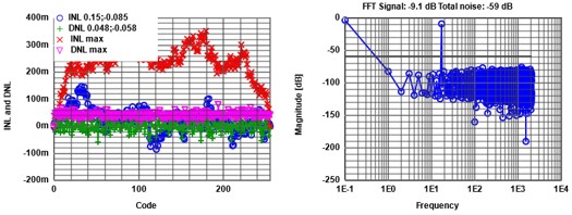
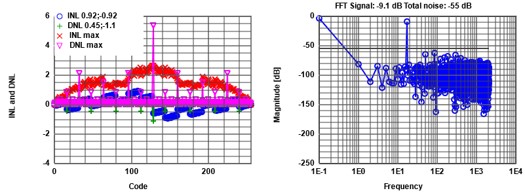
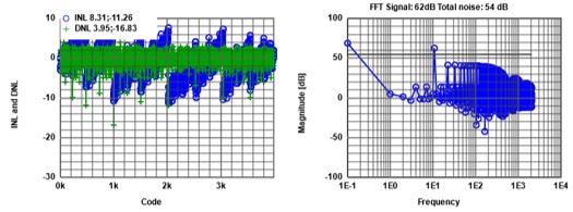
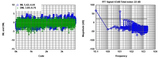
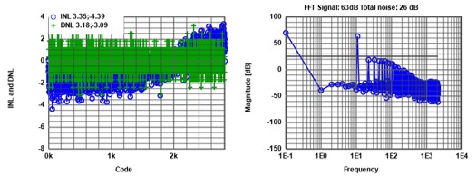
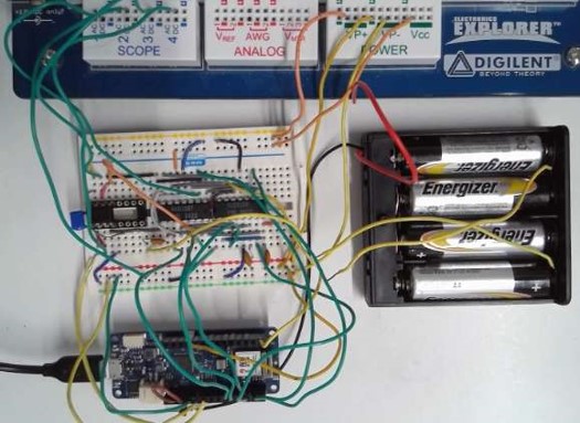
A serial C DAC has a minimum number of components. This structure makes it easy to simulate, realize, characterize and to study error correction. This paper presents a discrete 12 bit serial C DAC with digital error correction. Theory, high level (JavaScript), low level (LTSPICE) simulations, a real circuit and low cost measurements and error correction using an Arduino board are presented. Comparison of theory, simulation and measurement gives deeper understanding of DAC leading to better circuits and improved characterization methods. The measurements show INL, DNL below 4 and FFT with 46.5 dB SNQR which gives 6.5 ENOB at 33 Hz sampling frequency of a 12 bit DAC. Hardware cost are below 100 Euro without an oscilloscope for detailed signal measurements.

Keywords - serial DAC, circuit simulation, characterization, INL, DNL, SNR, error correction

I. INTRODUCTION


Data converters are very important elements connecting physical world to electrical world allowing digital signal processing. The quality of digital processing depends on the performance of the data converters. Therefore understanding and measurement of the quality of data converters allows to build high performance digital systems.

The resolution of data converters is limited by offset error, gain error, INL, DNL and SNR. The IEEE standards 1057 and 1241 are applicable for data converters. For high resolution data converters a lot of effort is required to calculate and measure these numbers. Unfortunately the relationship between the circuit configuration, faults and changes in these parameters is not easily determined. In the literature there is only limited data connecting circuit faults and errors to patterns in INL, DNL and SNR. A direct link between INL and spectrum is mathematically difficult. There are limited examples showing improvements of digital error correction [1, 2, 3]. Therefore publicly available tools to study these effects are very interesting.

Test and characterization engineers can use these tools to be able to prepare very early in the design process a proper test and characterization method. Simulations can be directly transferred to test. Additional tests can be simulated before hardware is available. Test data analysis can be prepared using available simulation data. Direct comparison of simulated and measured data leads to verification of the device and the test environment.

Simulations are valuable tools to understand theory by implementing equations and exploring variations. For circuit simulation SPICE variants (LTSPICE, PSPICE, Multisim) are used. Due to the large number of bits low level circuit simulation of data converters is very slow and requires a lot of memory and computing power. High level simulations are used to estimate data converter performance and understand conversion limitations. For high level simulation tools like MatLab Simulink or a programming language like C are used. These tools cost money and it is difficult to document simulation setup and results. This paper presents a low cost serial charge sharing DAC: schematic, high level simulation, practical realization., measurement and characterization.

A serial DAC is a simple, low component count easy to understand DAC [4]. Figure 1 shows a serial DAC (C1, C2, CLK1, CLK2) with sample and hold (X1, X5, C3, CLK3).


Fig. 1. A serial DAC with sample and hold

Data is serially latched with CLK1 in C1 (LSB first). Charge is shared between C1 and C2 with CLK2 activated. This cycle is repeated for each bit (serial). At the beginning CLK1 and CLK2 are active to put 0 V on both capacitors. The sample and hold circuit (preamplifier operational amplifier X1, switch CLK3 X5, operational amplifier X6) stores the output voltage. This circuit in principle could have infinite resolution for infinite number of charge sharing cycles. To calculate the final output voltage a charge computation is done:

Q = C · V
C2 · Vx2(n) + C1 · D(n) = Vx2(n+1) · (C1 + C2)
Vx2(n+1) = (Vx2(n) · C2 + C1 · D(n))/(C1 + C2)
with C1 = C2
Vx2(n+1) = 0.5 · Vx2(n) + 0.5 · D(n)
Vx2(n+1) = 0.25 · Vx2(n-1) + 0.25 · D(n-1) + 0.5 · D(n)
\( V_{out} = \sum_{k=0}^{nBit-1} 2^{-nBit+k} D(k) \)

The equations show the binary weight of the data inputs. This is a binary weighted DAC having a very low component count. Practical limits of this circuit are the precision of the capacitances C1 and C2, the leakage of the switches (back bias of transistors) and the leakage, offset and non linear gain of the operational amplifier. The precision of the matching of the capacitances have to be below 1 LSB. For a 16-bit DAC this would be 1/65536 = 15.2 ppm. Thermal noise of the R of the switches and operational amplifiers noise are also limiting the maximum resolution.
In the following sections first the LTSPICE simulation circuit with input signal generation for ramp and sine signals is presented. Open access internet pages are used to read and evaluate LTSPICE data [7]. The code for these pages is freely available at no cost. Due to the slow LTSPICE simulation and to model DAC errors properly an internet based JavaScript high level simulation is presented. All internet pages can also be run locally on a computer and source code can be modified to study other effects and architectures. Next the circuit is realized using an operational amplifier, NFET and PFET arrays and an Arduino board. Realization can prove the match between theory, simulation and real circuit and can highlight missing model assumptions. Then measurements of ramp and sine signals give INL, DNL, FFT, SNR and ENOB. Errors showed additional challenges of a real circuit and lead to error correction to improve ENOB. Finally results are discussed.

II. LTSPICE simulation

For simulation with LTSPICE (no cost program) serial digital data for a ramp and sine signal has to be generated. An ideal model of a 4 bit pipeline ADC and a switch matrix is used to generate the appropriate input signals easily. Figure 2 shows the 8-bit serial DAC circuit. An ideal DAC is omitted on the picture, but implemented to have an ideal output voltage for comparison. The resolution is limited to 8-bit to get reasonable simulation times. Real transistor models and operational amplifier models are used. Low frequency clock signals (tCK = 60 µs) are used since the practical circuit is also operated at low speed.


Fig. 2. LTSPICE test circuit

Care has to be taken to limit the raw output data file size with a save statement and to control precision with .option plotwinsize=0.

First an up/down ramp is used to have minimum settling time for accurate output values. The DAC output comes one cycle later than the input data. Care has to be taken that all codes are exercised and generate an output value. The circuit for download and simulation is available on a website [7].

Ramp simulation for INL and DNL


Figure 3 shows the INL, DNL of LTSPICE simulation (10 MB file size) after processing with JavaScript [7] tool in the browser.


Fig. 3. INL and DNL of LTSPICE ramp simulation

LTSPICE writes data with varying step size. Output data has to be filtered with sampling times. From this raw ramp data minimum and maximum is extracted. Real step size LSB is calculated:

LSBreal = (Maximum - Minimun)/NSteps

An ideal curve compensating for offset (Minimum) and gain error is generated:

OUTideal(i) = Minimum + i*LSBreal
and INL and DNL are computed:
INL(i) = (OUT(i) -OUTideal(i))/LSBreal
DNL(i) = (OUT(i)-OUT(i-1)-LSBreal)/LSBreal

All these steps are automatically done by JavaScript at client side in the browser. A graph is generated as displayed in figure 3. Maximum DNL of 1.5 and INL minimum of -0.8 can be seen reducing the effective number of bits. The program works up to a few million data points.

The circuit has a big error step at MSB switching limiting the resolution of the DAC. The effective number of bits is reduced.

The pattern of INL and DNL is typical for binary weighted data converters [6]. The DNL has a maximum at the center and can be up to 2 times the INL maximum error. DNL peaks can be seen only at multiples power of 2 bit switching. Higher order bits contribute higher to DNL error. A mismatch between the capacitances C1 and C3 or added capacitance of the CMOS transistor switches can lead to this pattern.

Sine simulation for FFT and SNR


An 8-bit DAC needs at least 256*4 points for FFT due to changing slope of a sine signal and an odd or prime integer number of periods to exercise all codes.

Having an integer number prevents FFT bleeding and windowing can be omitted. The simulation time tmeas is calculated as:
tmess = 1024 * 480 µs = 491.52 ms
having Nperiod = 13 periods gives a signal frequency of:

fsignal = Nperiod/tmess = 26.44856771 Hz.

The raw output data is evaluated with the same web page as ramp data. Start time 0, stop time 491.7E-3 and time step 480E-6. Figure 4 shows the resulting FFT mapping the DC content to a frequency of 0.1. Numbers for signal and noise level are shown at the top of the graph. Total noise level is shown as a line. The number of FFT points can be easily extracted from the maximum frequency as 2* 512 = 1024. To be able to asses an FFT the number of points determine the total noise, since all noise bins have to be summed up for total noise.


Fig. 4. FFT of the simulated serial C DAC

The signal can be seen at frequency 13 with -3 dB magnitude, total noise is -50.14 dB and biggest harmonic HD3 at -55.67 dB below an expected total noise level of
-3 dB -1.76 dB - 8*6.02 dB = -52.92 dB.

The total noise level can not be extracted easily from the FFT graph and needs some computation which is done by the web page in JavaScript at the client. Without the highest harmonic HD3 the total noise level is -51.65 dB. The -3 dB shows the rms value of the 1 V amplitude. The tool gives a table with the frequencies in order of signal magnitude (Table I).

This allows to look at the signal to noise level (47.29 dB) and the impact of harmonics. The effective number of bits can be calculated from this table as:

ENOB = (signal level - (total noise level) - 1.76 dB)/ 6.02 dB
ENOB = (-3 dB - (-50.29 dB) - 1.76 dB)/ 6.02 dB = 7.56

TABLE I. FFT MAGNITUDE RESULTS

FrequencySignal magnitude dBTotal noise magnitude dB
0 -0.04 -3
13 -3 -50.14
39 -55.67 -51.65
143 -63.56 -51.94
299 -65.98 -52.11
91 -66.28 -52.28

The ideal sine signal with 3V amplitude at the LTSPICE input with the ideal DAC was simulated as sanity check for comparison, shows no visible harmonic and gives

ENOB = (0.51 dB - (-49.1 dB) - 1.76 dB)/ 6.02 dB = 7.78

The first highest harmonic for an ideal signal is at frequency 447 with -65.33 dB. The simulation shows harmonics not limiting ENOB but the total noise. LTSPICE ideal DAC accuracy is still not showing the full ENOB = 8.

Based on this LTSPICE model circuit improvements and characterization can be easily done at no cost. Unfortunately for larger number of bits the simulation time and data size becomes quite big. A 16 bit simulation stopped after 84% of simulation after 10 h and 1.6 GByte file size due to lack of virtual address space on a system with 16 GByte main memory. A high level simulator is needed for faster analysis. A high level simulator shows also understanding of error sources by implementing the equations correctly.

III. JAVASCRIPT DAC SIMULATION

An Internet webpage [7] with a Javascript simulator was created to be able to study DAC errors faster (Figure 5). Unit or binary element DACs with different number of bits can be selected with random or systematic element error. Additionally a random noise measurement error can be added. Typical INL, DNL charts are generated. For FFT the number of points and number of periods of a test signal can be selected. Sine signal can have non integer and non prime number of periods. Effects on FFT with and without windowing can be studied. This can give a test engineer a feel for typical measurement errors and impact on results. Figure 5 shows the user interface and a result for an 8 bit binary element DAC with systematic error of -0.0065. INL and DNL is provided for one random error run and absolute INL and DNL maxima for a user defined number of runs. The QR code allows to access the internet page directly. Also some error correction method is implemented as presented later.

The typical INL, DNL pattern of a binary element DAC can be seen again and the FFT showing a harmonic. The values were chosen to match the LTSPICE simulation. A table with FFT magnitude values is also generated (Table II).


Fig. 5. Javascript Internet page with DAC Error simulation

TABLE II. FFT MAGNITUDEOF BINARY DAC WITH SYSTEMATIC ERROR

FrequencySignal magnitude dBTotal noise magnitude dB
13 -9.04 -54.88
39 -59.57 -56.69
299 -68.1 -57.01
91 -69.44 -57.27

The SNR of the simulation is -9.04 dB - (-54.88 dB) = 45.84 dB a little less than LTSPICE simulation. The first biggest visible harmonic (39) is still below total noise level. The next figures (Figure 6, 7) show the results for a random error of 0.01 for unit element and binary element DACs. The INL graph shows also the maximum of INL and DNL of 16 different random runs giving a worst case scenario.


Fig. 6. Random unit element DAC Error simulation

The simulation results change each run time due to the randomness of errors. It is possible to see typical patterns due to the architecture. INL of the unit element DAC can have one or more bumps, DNL is much lower and more random.


Fig. 7. Random binary element DAC Error simulation

DNL peaks are much bigger at the binary element DAC and INL shows a sawtooth pattern. FFT of the binary element DAC show a high harmonic due to the high DNL value. It is very easy to locate errors of the binary element DAC looking at the DNL and to correct them. Positive DNL determine the minimum step size, negative DNL causes code loss which can be corrected.
Only the binary element FFT shows visible harmonics. The bumps of the unit element DAC are too small to generate harmonics. It is interesting to vary the random error and look at many runs to observe the visibility of harmonics. The total noise will always be affected by INL, DNL error. The total noise of a binary element DAC is bigger than the unit element DAC with the same random error.
A systematic error can be applied to look at typical worst case INL, DNL and FFT patterns. Table III shows a summary.

TABLE III. SYSTEMATIC ERRORS, INL, DNL, SNR AND SDR

Type Systematic error INL, DNL max Magnitude Harmonic dBSNR without Harmonic dB
Unit0.000010.08HD2: -7949.74
Unit0.00010.8HD2: -5946.86
Binary0.0020.48HD3: -76.2449.5
Binary0.012.2HD3: -59.5245.31

Binary weighted topology:

\( \sigma_{INLmax} = 2^{0.5 \cdot B -1} \cdot \sigma_{Error} \)
\( \sigma_{DNLmax} = 2 \cdot \sigma_{INLmax} \)

Unit element topology:
\( \sigma_{INLmax} = 2^{0.5 \cdot B -1} \cdot \sigma_{Error} \)
\( \sigma_{DNLmax} = \sigma_{Error} \)

A σError gives for a 8-bit unit element DAC σINLmax = 8 · σError and for a binary element DAC σDNLmax = 16 · σError

Unit element DACs with systematic errors generate 2nd hamonics, binary element errors generate 3rd harmonics. Since there are more unit elements needed than binary elements, smaller systematic errors can cause a harmonic.

IV. DAC CIRCUIT MEASUREMENT

To allow comparison between theory, simulations and measurement the circuit was built and measured. For cost reasons an Arduino board was used for control and data acquisition. It is very cheap, easy to program, has a 12 bit DAC and ADC for voltage acquisition and reference and enough digital pins to operate the switches and data input at 3.3 V. Measurement data is transfered via the serial interface to the PC. The sampling speed is very slow.

The serial DAC needs only a few components and is very simple. It was build with one opamp IC 272, one ALD1106 and one ALD1107 integrated circuit with 4 NFET and 4 PFET transistors each as switches and 3 10pF capacitances. Beside the 3.3 V the operational amplifier need extra voltages (5 V, -1.5 V), which were provided via battery or a Electronic Explorer power supply to amplify a signal in the 0 to 3.3 V range. Figure 8 shows the final set up.


Fig. 8. Serial C DAC circuit realisation with Arduino and power supply

Data processing is done via another JavaScript tool. It is planned to have a local nodejs server controlling the Arduino via serial interface and providing a better web interface for the user. This would improve characterization capabilities. The Arduino program is also available on the web site.
The internal waveforms for circuit verification were measured with an oscilloscope in figure 9. C1 (yellow) shows the sampling every 29 ms. C3 (red) shows the internal node of the second capacitance C2 (blue). After a long initialization of 20 ms the data is transferred serially to the capacitance. C2 is a zoomed waveform of C3, which shows charging and discharging of this capacitance during the charge equalization times probably due to leakage. This is one reason for the steps. C4 (green) shows output voltage changing at the sampling with CLK3 and C1 signal.

The breadboard allows easy circuit modification and access to all signals. The Arduino environment provides easy change of CLK signal sequence, voltage levels and provides data transfer to a PC.


Fig. 9. Internal signals of serial DAC

Since the basic functionality was confirmed noise measurements were done and compared to averaging results (Table IV). Averaging of 16 values at code 2040 gave an average value of 2238 and shows a good compromise between accuracy and acquisition time. 64 would give a delta below 1, but was not used in this work due to time constraints. An automatic test sequence would allow application of higher averaging values. Theory states a gain of 10 log(OSR) in resolution for averaging. This can be seen in the reduction of standard deviation by a factor of 2 for an oversampling ratio of 4.

TABLE IV. AVERAGING OF SAMPLES AND DELTA FOR CODE 2040

Samples 1 4 16 64 256
Min 2223 2234 2237.4 2238.0 2238.3
Max 2250 2241.8 2239.7 2238.9 2238.5
Delta 27 7.75 2.31 0.91 0.16
Npoints 1024 256 64 16 4
Standard Deviation 2.33 1.21 0.54 0.27 0.07

Next full scale and mid scale settling time was measured. For full scale settling time all bits are changing from 0 to 1 or vice versa. Figure 10 shows only the difference to final value of this measurement with and without averaging.


Fig. 10. Code error for full scale settling time

At least 2 samples are needed until the final value is reached. It is expected that large voltage changes will effect measured SNR of this set up. The circuit has some memory effect and should be improved. On the other hand this error can be measured and used in studying error correction.

Next ramp measurements were done and offset (20 codes) and gain error observed. The output started with a code of 20 and reached 4095 for a input code of 4040. The full resolution of 12 bit could not be reached in this set up with these values since 20+55 codes are missing.

First ramp measurement for 12 bits gave INL between 8.31 and -11.26 and DNL between 3.95 and -16.83. FFT gave 62 dB signal and 54 dB total noise as seen in figure 11.


Fig. 11. Raw measurement INL, DNL and SNR

Range matching is one important feature of DAC testing. Therefore it is interesting to see what happens if the sine signal is overshooting and top and bottom are cut off. Table V shows a typical evaluation. A cut off of 4 codes affects the signal to noise behaviour by 6 dB. During test only a slightly smaller range than minimum and maximum code should be tested.

TABLE V. FFT MAGNITUDE OF BINARY DAC WITH SYSTEMATIC ERROR

Min MaxSignal magnitude dBTotal noise magnitude dBCut off
100389962.56 -10.6 0
400350061.72 40.17 300
200379962.44 28.64 100
132386862.54 17.13 32
116388362.55 9.94 16
108389162.56 2.79 8
104389162.56 -3.77 4

V. ERROR CORRECTION

A calibration or error correction can be done based on the ramp INL, DNL data. Here 2 schemes are discussed. First only 31 code changes of multiples of 128 for the 5 MSB bits are corrected. Secondly a lookup table is constructed. Error correction always reduces the number of possible codes. Therefore the sine range and offset have to be adjusted.

Due to the pattern of the binary DAC transition voltages can be defined, where an offset has to be added to the DAC code value. In this example of a 12-bit DAC 7 correction values were added for the 3 MSBs.

The correction values C(i) can be extracted from the ramp measurement and added Csum(i).A comparator compares the input code with the transition voltages Vt(i) and applies the correction values C(i). For Vt(i) the sum of the correction code has to be subtracted.

In this example the 3 MSB give the transition voltages:
Vtn = 511, 1023 1535, 2047, 2559, 3071, 3582
From the ramp measurement the following correction factors were taken:
C = 6,10,5,12,4,8,5
At each transition voltage the correction factors are added up:
Csum = 6,16,21,33,37,45,50
Each transition voltage changes due to the Csum(i):
Vt = 511, 1017, 1519, 2014, 2522, 3026,3532
In the control program the input code is compared with the transition voltages and correction Csum(i) is added. 3903 Codes remain, DNL and INL is improved (Figure 12).


Fig. 12. Improved custom calibration INL, DNL and SNR

Secondly lookup calibration can be done. A lookup table is created using sorted pivot operation on ramp data displaying for each output code the maximum input code. Then a lookup for each possible input code is done for the maximum input code. In this example 2840 unique codes remained (Figure 13).


Fig. 13. Improved lookup calibration INL, DNL and SNR

Table VI shows the results for ENOB INL and DNL for an ideal 12-bit sine signal, the uncalibrated serial DAC sine signal, custom and lookup calibrated DAC sine signal.

TABLE VI. CALIBRATION SNR, INL AND DNL
Ideal sineNo calibrationCustom calibrationLookup calibration
Periods11111111
Signal magnitude dB63.0162.3962.9263.01
Total noise magnitude dB-10.954.4122.2725.74
ENOB12.01.06.55.9
INL min0 -12-6-6
INL max0 853
DNL min0 -16-6-3
DNL max0 556
NFFT4k4k4k4k

It was also investigated how the number of FFT points NFFT is affecting signal to noise ratio.

TABLE VII. FREQUENCY, NUMBER OF FFT POINTS AND SNR

Ideal sineCustom calCustom calCustom cal
Periods11111111
Signal magnitude dB63.0162.8862.9262.92
Total noise magnitude dB-10.9333.0322.2711.37
ENOB12.04.76.58.3
NFFT4k1k4k16k

More FFT points decreased the frequency of the signal increasing the ENOB. This was confirmed measuring with different frequencies (Table VIII).
TABLE VIII. FREQUENCY, PERIODS AND SNR

PeriodsSignal magnitude dBTotal noise magnitude dBENOBNFFT
116232.814.61k
4361.6841.33.11k
4461.6841.373.11k
17959.4244.512.21k

As expected from the full settling time measurement big changes in voltage present in high signal frequency measurements can cause this. This would also be a typical behaviour in the presence of jitter. Since the board is generating the signal synchronized to the the ADC data acquisition there should be no jitter present. More research in this area to improve the circuit is needed.

VI. SUMMARY AND OUTLOOK

A binary element serial C DAC is presented with theory, low level, high level simulation, circuit realization, analysis tools and characterization. Typical characterization steps were done using online web based JavaScript internet tools for analysis. The circuit is very cheap to built and has enough errors to be an interesting subject for study.

The acquisition of 1k data points took 108 s, 60 ms and 30 s for LTSPICE simulation, JavaScript DAC simulation and measurement. With the number of bits the simulation times increase exponentially. A high level simulation is very versatile and fast, but can only model what is found via LTSPICE simulation or measurement. Correlating data confirms understanding of the DAC circuit.

JavaScript tools were also used to read and analyze LTSPICE data. INL, DNL from ramp data and FFT and SNR of sine data are automatically calculated and displayed.

Open access internet based tools makes it very easy to analyze the data and do simulation. The underlying JavaScript code can be locally copied and modified for different application and failure modes. Even big data amounts can nowadays be analyzed in the browser in a short amount of time.

All characterization steps with pitfalls were presented: Noise (base code), averaging (increased number of bits), settling time (full scale and mid scale), ramp test (start, stop codes), sine test (offset, range, NFFT, odd or prime number of periods), FFT, SNR and error correction.

Two error correction procedures for binary element DACs were presented in detail and results discussed. The error correction showed a significant improvement in INL, DNL and SNDR. Since the correction procedures were also implemented in JavaScript the detailed code can be studied in detail and improved. The simple circuit shows typical DAC errors and can be easily modified for experiments. This makes characterization of DACs easier and accessable.

Final measurement data showed INL, DNL below 6, SNR of 46.5 dB and ENOB with error correction. Improvement of error correction was 32 dB or 5.5 ENOB.

Future work will improve the tool chain and enable more interactive web based DAC characterization. Variations of the circuit to operate from a battery supply and have higher voltage CLK levels are planned to study circuit limitations. More analysis of the circuit is needed to improve the circuit, decrease the error, increase the resolution and speed up the sampling frequency.

REFERENCES

[1] A 14-bit 1.8-V 20-mW 1-mm CMOS DAC, Mika P. Tiilikainen, Member, IEEE, JSSC, 2001
[2] A 14-bit 200MS/s Current-Steering DAC Achieving over 82dB SFDR with Digitally-Assisted Calibration and Dynamic Matching Techniques, Jen-Huan Tsai, Yen-Ju Chen, Yan-Fong Lai, Meng-Hung Shen and Po-Chiun Huang, 2012
[3] D. A. Mercer, "Low Power Approaches to High Speed CMOS Current Steering DACs," IEEE Custom Integrated Circuits Conference 2006, 2006, pp. 153-160, doi: 10.1109/CICC.2006.320868.
[4] Mismatch-shaping serial digital-to-analog converter, Steengard, Moon, Temes, 1999
[5] R. Suarez, P. Gray, and D. Hodges, "All MOSFET charge- redistribution analog-to-digital conversion techniques-Part II", IEEE Journal of Solid-State Circuits, vol. SC-10, no. 7, pp. 379-385, December 1975
[6] C. Lin and K. Bult, "A 10-b,500-MSample/s CMOS DAC in 0.6 mm2," IEEE Journal of Solid-StateCircuits, vol.33, pp. 948- 1958, December1998.
[7] J. Vollrath, Low cost serial DAC simulation, realization, error correction and characterization, https://personalpages.hs-kempten.de/~vollratj/Projekte/ CSerial.html


Dr. Ing. Joerg E. Vollrath received 1989 his Dipl. Ing. and 1994 his Ph. D. in electrical engineering, semiconductor technology at the University of Darmstadt, Germany. Since then he worked for the memory division of Siemens and Infineon Technologies and Qimonda in various locations in the USA and Germany. He is now a Professor for Electronics at the University of Applied Science, Kempten, Germany. His expertise and interest lies in the field of design of analog and digital circuits, programmable logic, test, characterization, yield, manufacturing and reliability. He has published 22 papers and has currently 23 patents.

Tools

Arduino Sketch

Click on the schematic and download all the listed files locally.
Then run LTSPICE.
Figure 1: A serial DAC with sample and hold

Figure 2: LTSPICE test circuit

Processing LTSPICE output files


Save only one voltage over time using the '.save V(Vx)' statement.
Read LTSPICE files

Simulate unit element and binary DAC with errors INL, DNL, FFT and SNR


Simulate DAC

Evaluate measurement data with INL, DNL and FFT


Read measurement data and calculate INL, DNL, FFT

Interface Electronics Lecture


15 weeks of 90 min lecture and 90 min laboratory.
Data converter lecture with more content and tools

References


[1] A 14-bit 1.8-V 20-mW 1-mm CMOS DAC, Mika P. Tiilikainen, Member, IEEE, JSSC, 2001
[2] A 14-bit 200MS/s Current-Steering DAC Achieving over 82dB SFDR with Digitally-Assisted Calibration and Dynamic Matching Techniques, Jen-Huan Tsai, Yen-Ju Chen, Yan-Fong Lai, Meng-Hung Shen and Po-Chiun Huang, 2012
[3] D. A. Mercer, "Low Power Approaches to High Speed CMOS Current Steering DACs," IEEE Custom Integrated Circuits Conference 2006, 2006, pp. 153-160, doi: 10.1109/CICC.2006.320868.
[4] Mismatch-shaping serial digital-to-analog converter, Steengard, Moon, Temes, 1999
[5] R. Suarez, P. Gray, and D. Hodges, "All MOSFET charge- redistribution analog-to-digital conversion techniques-Part II", IEEE Journal of Solid-State Circuits, vol. SC-10, no. 7, pp. 379-385, December 1975 [6] C. Lin and K. Bult, "A 10-b,500-MSample/s CMOS DAC in 0.6 mm2," IEEE Journal of Solid-StateCircuits, vol.33, pp. 948- 1958, December1998.

[8]C. Mangelsdorf, "The Other ADC Test [Shop Talk: What You Didn't Learn in School]," in IEEE Solid-State Circuits Magazine, vol. 14, no. 1, pp. 16-96, winter 2022, doi: 10.1109/MSSC.2021.3126985.