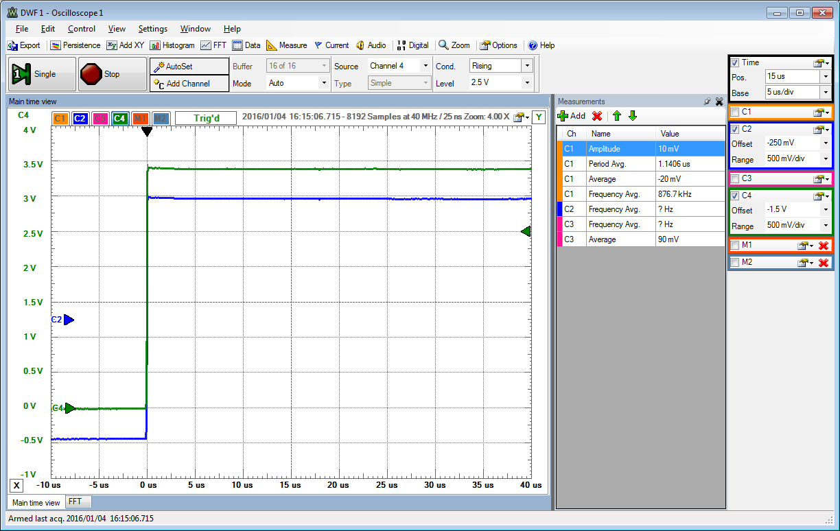
SAR operation snapshot
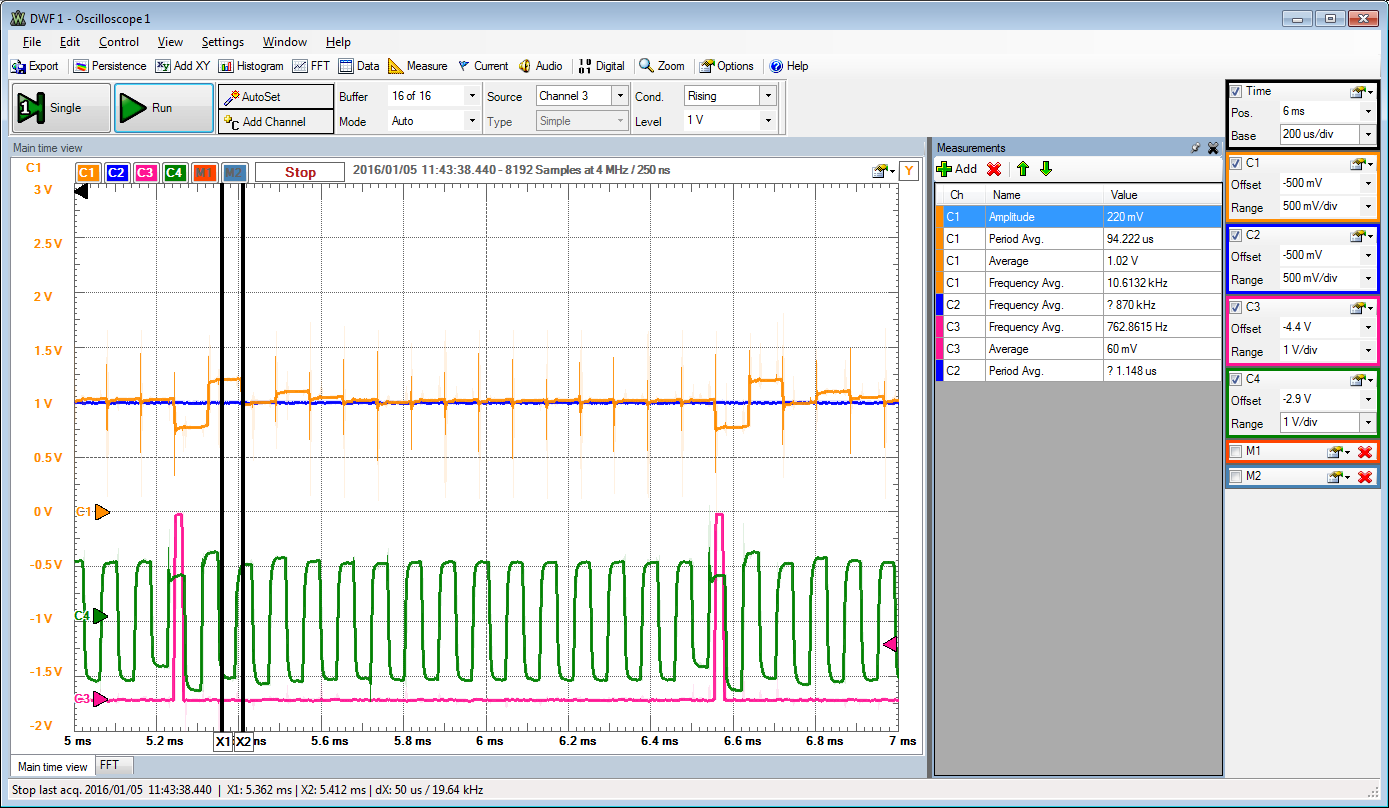
C1: DAC output after SH.
C2: AWG1 input signal
C3: SH start of conversion, sample and hold signal.
C4: DAC output signal
DAC output works only good with oscilloscope(R = 1 MOhm, C = F) at output.
It can be seen how 16 steps are done during succesive approximation.
Settling time and ramp measurement
Output waveform and digital input signals can be measured. Digital input signals should be rectangular and reach full level. Weak digital drivers can limit settling time.Since the oscilloscope has a 10 Bit ADC, an 8 Bit C2C DAC was used (sw6..5 = 11).
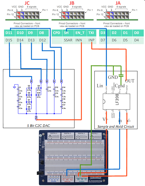
Only the C2C DAC was connected to the outputs of the FPGA.
Settling time was measured for full level rising and falling and midlevel rising and falling for a sawtooth signal (sw4..3 = 10,01).

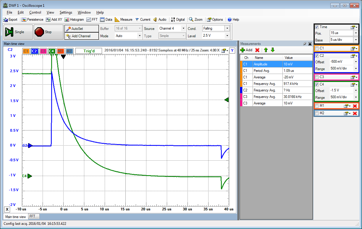
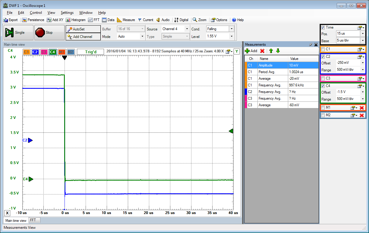
The worst case settling time can be observed at mid level switching.
Assuming an exponential capacitance charging curve a settling time of 40 us can be determined.
\( v(t) = V_{FS} \left( 1 - e^{-\frac{t}{\tau}} \right)\)
If it takes \( t_1 = 4 \mu s \) to reach \( 0.5 V_{FS} \), it takes \( 2 \cdot t_1 \) to reach \( 0.75 V_{FS} \). 8 Bits need \( 8 t_1 = 8 *4 \mu s = 32 \mu s \) to reach a precision less than 0.5 LSB. The closest option is 40 us (sw2..0 = 011).
Ramp measurement
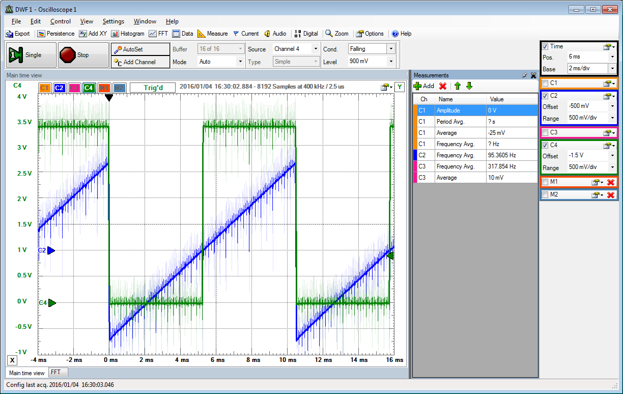
The oscilloscope records 8192 values at a time. Since the period of the sawtooth is 10.48ms this gives 4195 values. 16 values per level. Only the average of the last 3 values for each level are used for the DAC transfer curve.
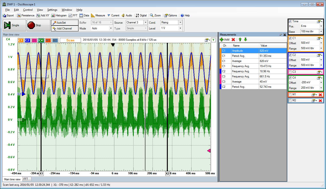
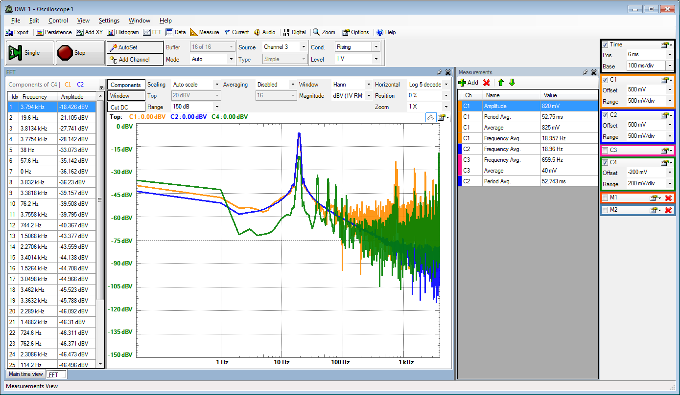
Spectral test of DAC
Using sw4..3 = 11 generates a sine wave for the DAC. This works only with 16 Bit mode, leaving driving bits 0..7 at 0V.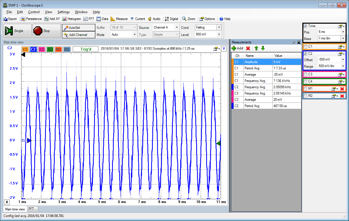
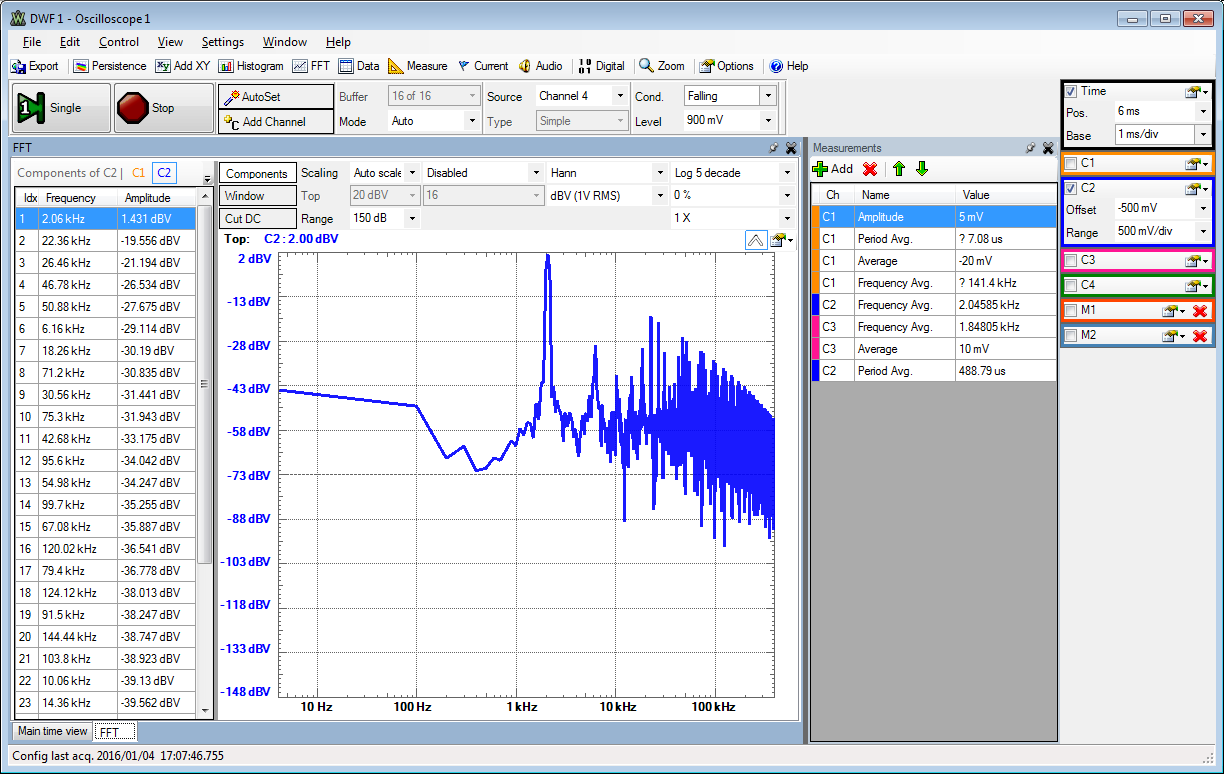
The signal strength is 1.42 dbV at 2.06kHz and the next highest peak is at -19.5 dbV at 22.36kHz.
How is a DAC spectral test done and signal to noise ratio calculated?
Sample and hold operation
There is a sample and hold circuit needed to keep the input voltage during conversion constant, controled via signal SH.The C2C DAC eliminates DC component. therefore positive and negative voltages will occur.
sw7 is used to invert the DAC output for half the cycle reducing the number of effective bits by one and eliminating a DC component. To feed this signal to the input receiver of the FPGA it is necessary to use a second sample and hold circuit which transfers only positive voltages to the FPGA. The second sample and hold is controled by signal SH1.
First clock/control feedthrough is measured.
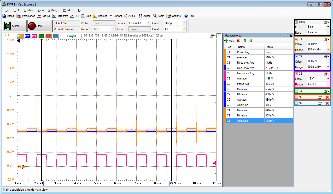
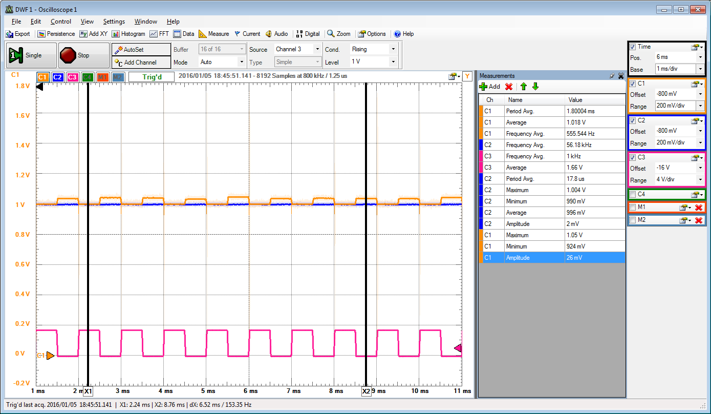
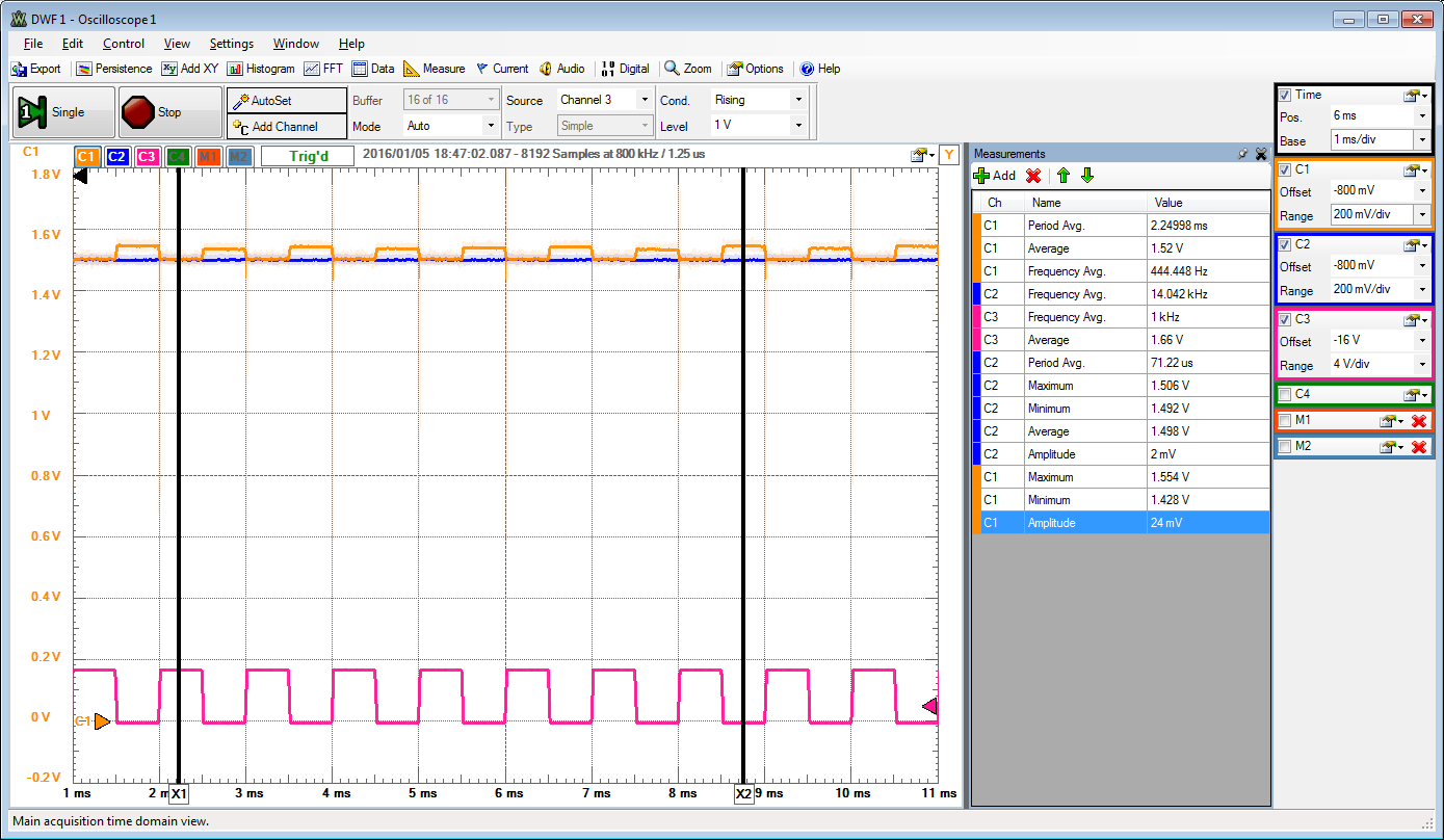
C1: Signal after SH.
C2: AWG1 constant input signal
C3: SH control signal.
0.5 V, 1.0 V, 1.5 V input signal 26 mV amplitude output.
The sample and hold adds 50 mV to the signal.
Is this result depending on the load capacitance?
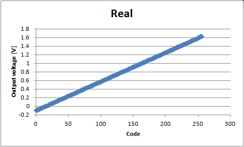
SAR transfer curve
Setup: 1.3ms per 16 Bit sample. Range: -90mV..1.63V8 Bit sampling 10 values per Bit gives accuracy of 0.1 LSB.
Time: 2560 * 1.3ms = 3.32s
Frequency ramp: 0.15Hz
UART transmits 2 hex values per sample.
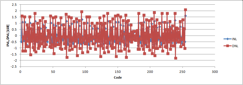
Effective resolution should be 7 Bit.
Spectral test
1.3ms per sample. 8 bit 256 values take 16 * 256 = 4096 samples. 5.3248 seconds. 101 periods gives 18.96 Hz for input sine signal.38400 Baud rate, 8 characters (1 Byte + 2 start stop) per value gives 38400/8/10 = 480 samples per second. The output code was transmitted twice giving a data rate of 240 samples per seconds.
Since 4096 samples were taken for FFT of digital output data (0..255) it took 16s. Therefore the base frequency code of 1 is equivalent to 0.0625Hz. The signal of 18.96Hz is then around 400.
Sine time signal:
x-axis: log SNR = 1.73 dB + 6.07 B dB + 10 log10( N / 2 )
B: Number of Bits
N: Number of samples = 16 * 2 B
N = 2048 -> 30 dB
There is bleeding because a non integer number of periods. Realistic noise level is -20dB + 36 dB = 16 dB. SNR = 30 dB - 16 dB = 24 dB gives ENOB = (24 dB - 1.73 dB) / 6.07 dB = 4 Bit.
Signal: 20 * log (256) = 48 dB