[1] B. Verbruggen, et al., “A 2.2mW 5b 1.75GS/s Folding Flash ADC in 90nm
Digital CMOS,” ISSCC Dig. Tech. Papers, pp. 252-253, Feb. 2008.
[2] Y.-S Shu, “A 6b 3GS/s 11mW Fully Dynamic ADC in 40nm CMOS with
Reduced Number of comparators,” Symp. VLSI Circuits, pp. 26-27, June 2012.VLSI 2012
[3] V. H. -C. Chen and L. Pileggi, “An 8.5mW 5GS/s 6b Flash ADC with Dynamic
Offset Calibration in 32nm CMOS SOI,” Symp. VLSI Circuits , pp. 264-265, June 2013.
[4] M. Miyahara, et. al., "22.6 A 2.2GS/s 7b 27.4mW time-based folding-flash ADC with
resistively averaged voltage-to-time amplifiers," 2014 ISSCC, San Francisco, CA, 2014, pp. 388-389.
Data converter performance parameters
Sampling frequency
Resolution, effective number of bits, signal to noise ratio (ENOB, SNDR)
Citation:
A figure of merit (FoM) is a useful tool for comparing the conversion efficiency of A/D converters.
This presentation reviews the make-up and composition of the most popular FoMs quantifying the tradeoff
between ADC speed, resolution and power dissipation.
In addition, it investigates the pertaining asymptotes and trends over time.
The obtained information allows us to quantify past progress rates and lets us speculate about the future.
A.M.A. Ali et al., "A 16-bit 250MS/s IF Sampling Pipelined ADC with background
calibration, JSSC, Dec2010
FOM1: Small numbers are better.
FOM2: Large numbers are better.
\( FOM_2 = 10 log(\frac{1}{FOM_1}) \)
This figure of merit takes into account best performance per part.
SNR is power of sine signal divided by noise power.
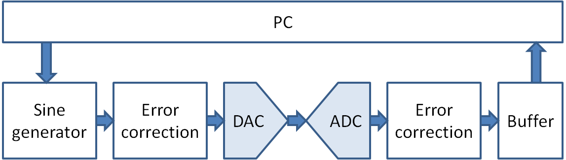
DAC ADC Measurement
DAC:
ADC:
N:
Offset Error:
Gain Error:
Investigations
DAC Bits
ADC Bits
N
Offset Error
Gain Error
Comment
3
3
1
0
0
Same number of Bits and no error
3
5
1
2
-20%
DAC is tested by ADC and shows a limited output range
5
4
1
2
-20%
ADC is tested by DAC and shows a limited output range
ADC and DAC same number of bits:
Total errors bigger than 1 LSB can be detected.
Offset and gain errors can lead to a reduced number of output codes.
It is not clear if ADC or DAC has errors.
ADC has more bits than DAC:
Only DAC is tested
INL, DNL errors of 2BDAC/BADC · LSB can be detected.
Offset and gain error can lead to a limited output range.
ADC has less bits than DAC:
Only ADC is tested.
INL, DNL errors of 2BADC/BDAC · LSB can be detected.
A range of DAC codes gives the same ADC output code. This is a histogramm test.
General remarks
Taking multiple measurement points per DAC code can look like a histogram test.
Noise can cause multiple ADC codes per DAC code.
A histogram test averages noise out.
Applying an operational amplifier (Opamp) can increase the resolution of ADC or step size of DAC
and adding an offset.
Using a voltage divider enables smaller DAC step sizes.
Characterization can then be done using multiple steps for sub ranges with different offsets.
DAC ADC Test Simulation
DAC X4 provides coarse steps, DAC X2 provides fine steps for ADC test.
For high resolution DAC test The DAC ouput can be amplified and an offset applied and the tested with the ADC.
Another possibility for DAC test would be to build a 2 stage multibit pipeline ADC.
DAC: (Ladder, R string, Interpolating,) Binary, R2R, C2C, C Serial
ADC: (Flash, Dual slope,) Pipeline ADC), SAR ADC, Sigma Delta
Comparator, Amplifier, Switch, Sample and Hold
Averaging, Interpolating, Serial, parallel
Offset, gain, INL, DNL, FFT, SNR, test, error correction and diagnosis effort
Calculate INL, DNL (Ramp test, Histogram test)
Analyze a FFT.
Recognize DAC, ADC architecture and calculate transfer curve.
Calculate RC for NBit and fbw for switch and sample and hold.
(Calculate amplifier and comparator requirements (gain, offset))