Droop compensating FIR filter
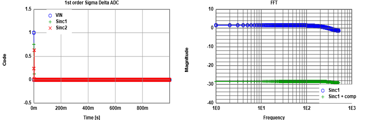
The graphs are generated by 1st order passive sigma delta JavaScript simulator.
Using a pulse input the FFT shows the transfer function of the system.
Droop of the signal can be seen for higher frequencies (blue curve).
The filter can compensate for part of it (green curve).
|
An droop compensating FIR Filter
[ http://www.cypress.com/file/123171/download ]
with a function: \( out(i) = \frac{-1}{K -2} in(i) + \frac{K}{K -2} in(i-1) + \frac{-1}{K -2} in(i-2) \) can be activated. This filter function can be implemented in an FPGA employing shift, add, subtract (using 2s complement) and multiply. Fractions are normalized with the word width of the signal. K values can be taken from the link above.
|

Experiments:
Show transfer function: Number of periods = 0, SINC1, SINC2, + comp FIR
Show transfer function: Number of periods = 0, SINC1, SINC2, + comp FIR
A second order active Sigma Delta ADC
An FFT with 8192 points can be made and VD can be extracted with
Read Raw File
. Start time 0; Stop time 81.92E-6; Time step 10E-9
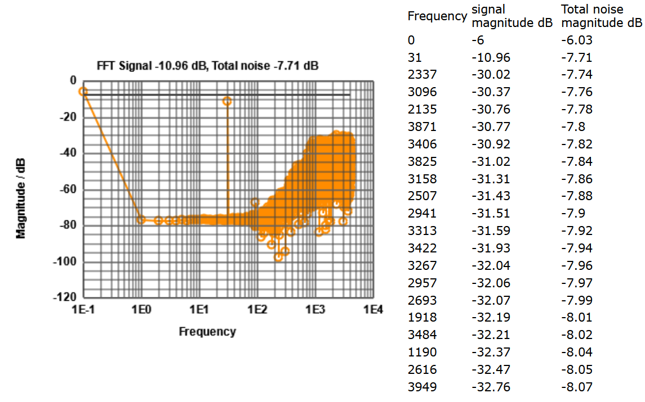
Figure: FFT of 1-Bit output signal.
Oversampling rate:
\( OSR = \frac{f_{CLK}}{2 \cdot f_{BW}} = f_{CLK} \cdot 2 \cdot 2 \pi R \cdot C = 100 MHz \cdot 1.5 \mu s = 150 \)
Between frequencies 100 and 1000 the noise increases by 50 dB as expected.
The corner freqeuncy of 100 is determined by the R = 5 kΩ and C = 10 pF values.
Frequency of 1 has a period T = 81.920 us and a frequency of fmin = 11.22 kHz.
\( f_{3dB} = \frac{1}{2 \pi R C} = \frac{1}{2 \pi 5 k\Omega 10 pF} = 3.2 MHz \).
Normalized
\( f_{3dBNorm} = \frac{f_{3dB}}{f_{min}} = 300 \).
The bigger RC is, the smaller gets the amplitude at the comparator.
For large RC values instability can be seen.
The comparator has to be more sensitive and has to have less offset.
. Start time 0; Stop time 81.92E-6; Time step 10E-9
Figure: FFT of 1-Bit output signal.
Oversampling rate:
\( OSR = \frac{f_{CLK}}{2 \cdot f_{BW}} = f_{CLK} \cdot 2 \cdot 2 \pi R \cdot C = 100 MHz \cdot 1.5 \mu s = 150 \)
Between frequencies 100 and 1000 the noise increases by 50 dB as expected.
The corner freqeuncy of 100 is determined by the R = 5 kΩ and C = 10 pF values.
Frequency of 1 has a period T = 81.920 us and a frequency of fmin = 11.22 kHz.
\( f_{3dB} = \frac{1}{2 \pi R C} = \frac{1}{2 \pi 5 k\Omega 10 pF} = 3.2 MHz \).
Normalized
\( f_{3dBNorm} = \frac{f_{3dB}}{f_{min}} = 300 \).
The bigger RC is, the smaller gets the amplitude at the comparator.
For large RC values instability can be seen.
The comparator has to be more sensitive and has to have less offset.
Switched capacitor circuits
|
Source: Baker, Mixed signal design, Fig2.35 |
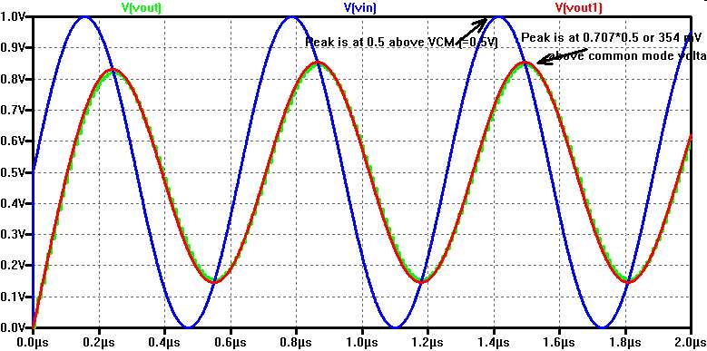 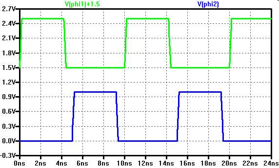 |
In switched capacitor circuits resistors can be replaced by capacitances.
The frequency of the non overlapping clock determines the value.
Capacitances can be fabricated with high accuracy and are less temperature dependent than resistors.
The simulation is done with ideal switches.
Comparison to resistor:
What is the average current?
dV = Vin - Vout
CI · dV = Q = Iavg · dt
\( I_{avg} = \frac{C_{I} \cdot dV}{dt} = C_{I} f dV = \frac{1}{R} dV = G dV\)
CI f = 1p · 100MHz = 0.1 mS = G
z-domain:
\( a = e^{-\frac{1}{ R C_F f}} = e^{-\frac{C_I}{C_F}} \)
\( H_{RC}(z) = \frac{Y(z)}{X(z)} = \frac{1-a}{1-az^{-1}} \)
Reference: Take the RC Low-Pass Filter to the Z-Domain
Second order active switched capacitor Sigma Delta modulator
|
Source: Baker, Mixed signal design, Fig 7.29 |
Cascaded (2-1-MASH) Sigma Delta ADC
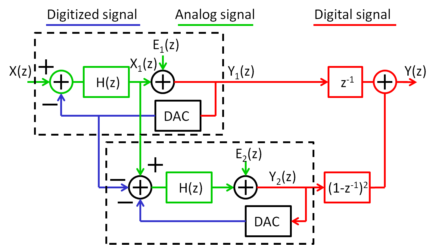
Idea
Quantify digitalization error further and correct in digital domain.
The signal and noise transfer function for a 2-1 MASH sigma delta modulator can be calculated:
\( Y_{1}(z) = z^{-2}\cdot X(z) + (1-z^{-1})^2\cdot E_{1}(z) \Rightarrow *z^{-1}\)
\( Y_{2}(z) = z^{-1}\cdot ( E_{1}(z)) + (1-z^{-1}) \cdot E_{2}(z) \Rightarrow *(1-z^{-1})^2 \)
\( Y(z) = z^{-1}\cdot Y_{1}(z) - (1-z^{-1})^2\cdot Y_{2}(z)\)
\( Y(z) = z^{-3}\cdot X(z) + z^{-1} \cdot (1-z^{-1})^2\cdot E_{1}(z) - z^{-1}\cdot (1-z^{-1})^2\cdot E_{1}(z) + (1-z^{-1})^{3} \cdot E_{2}(z)\)
The \(E_{1}(z)\) terms cancel out:
\( Y(z) = z^{-3}\cdot X(z) - (1-z^{-1})^{3} \cdot E_{2}(z)\)
Brandt, Wooley, A 50-MHz Multibit Sigma Delta Modulator
for 12b 2-MHz A/D Conversion, JSSC, p.1746-1756, Dec 1991
Digital z-Elements
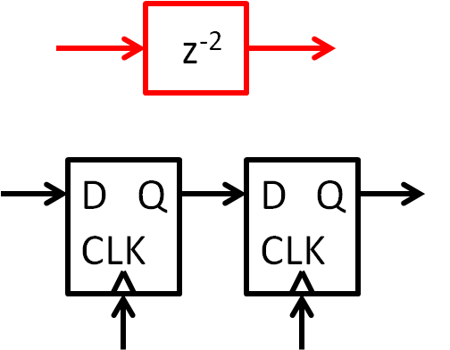
|
_2.png)
|
JavaScript, C: |
JavaScript, C: |
VHDL: |
VHDL: |
What bit width is needed?
What happens if bit width is increased?
What happens if bit width is increased?