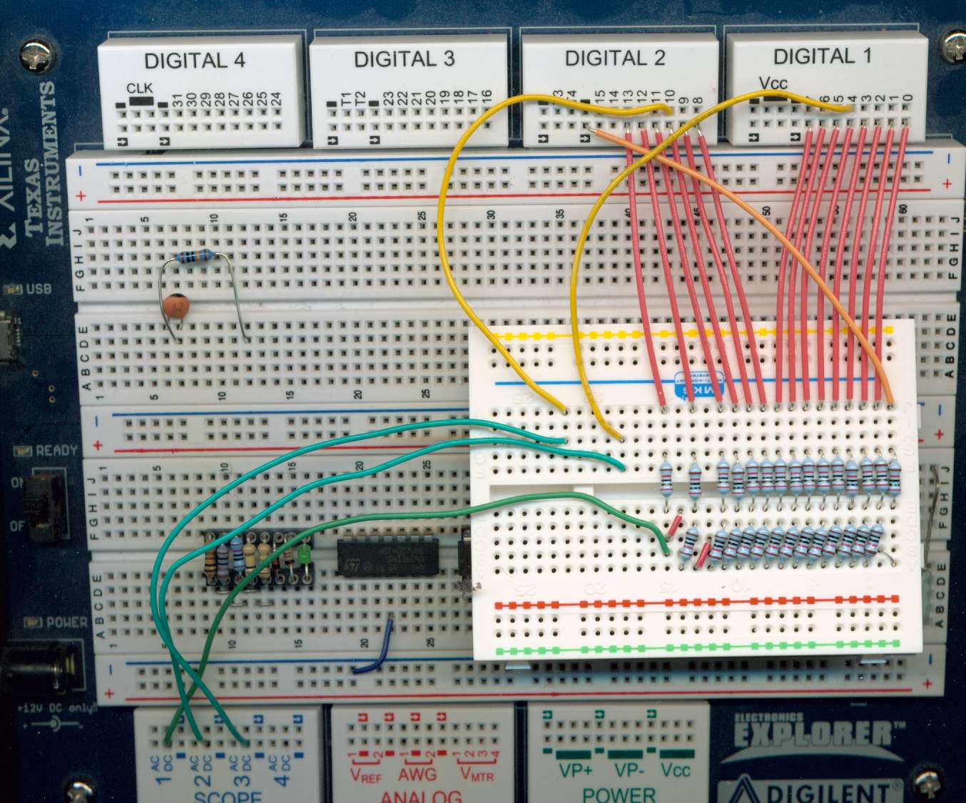
Solution:
There are only 200kΩ and 100kΩ resistors with 0.1% (200 Ω ; 100 Ω) accuracy available. The resistance of wiring is well below the needed tolerance (100 Ω). The accuracy is 1/1000 and barely sufficient for 10 Bit.
A typical student measurement is shown below:
| Name | R17 | R18 | R1 | R3 | R5 | R7 | R9 | R11 | R13 | R15 | R30 |
| R [kΩ] | 200 | 199.9 | 199.8 | 199.8 | 199.9 | 200 | 199.8 | 200 | 199.9 | 199.9 | 199.8 |
| Name | R19 | R2 | R4 | R6 | R8 | R10 | R12 | R14 | R16 |
| R [kΩ] | 99.9 | 99.9 | 99.9 | 99.9 | 99.9 | 99.9 | 99.8 | 99.9 | 99.9 |
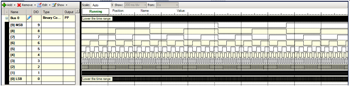
Start the pattern generator. Create a bus with D0..D9. Select a binary counter with push pull (PP) drivers. Select a frequency of 1kHz under parameter for the counter.
Make sure that the settling time of the signal is ok for a full level transition.
Since the oscilloscope has only 10-Bit resolution, you have to do multiple measurements.
Choose a vertical range of 50 mV/div. Set the Trigger to Channel 1 Rising.
Use the full vertical range of the oscilloscope to minimize error.
Channel 1 should show the output voltage, channel 2 and 3 should show D0 and D6.
Each measurement should give you data for 100 codes each having 80 values.
For a 10-Bit counting frequency of 1 kHz you have a time base of 10ms/div.
Export the measurement values (OSC1), D0 (OSC2) and D6 (OSC3) using the Export function. You can use D0, and D6 to synchronize your measurements with the input code.
Calculate the average output voltage per code using 64 values omitting output voltage values during settling time.
Solution:
The pattern generator for the ramp is shown below:
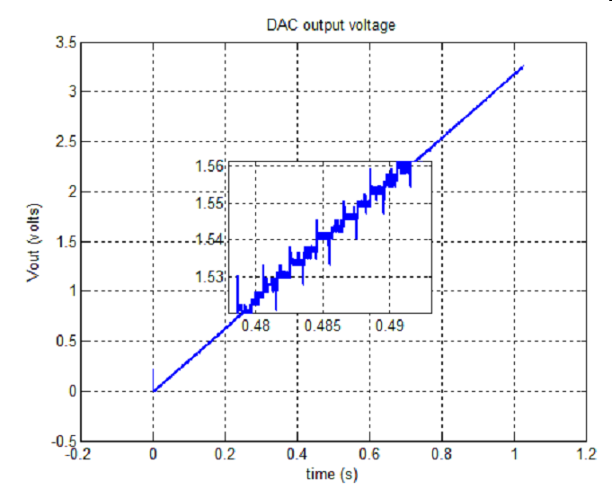
A typical functional screen shot is also shown:
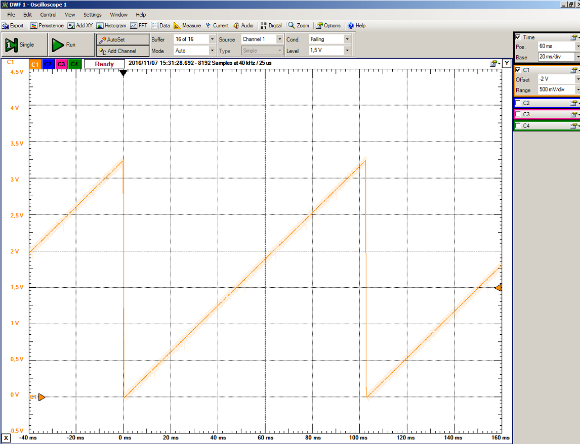
The y axis shows a range of 5 V. Having a 10-Bit ADC at the oscilloscope this would give a resolution of 5V/1024 = 5mV which is not sufficient for the 10-Bit DAC.
The challenge is to measure 1024 values with enough accuracy in a limited time frame.
The Vout(000) was measured as: Vout(000) = 5.7588 mV. (Offset)
The Vout(3FF) was measured as: Vout(3FF) = 3.2516 V. (Maximum voltage)
Both values have to have enough accuracy to calculate a correct LSB with at least 4 digits. Using less digits results in a increasing or decreasing INL because of accumulating rounding error when calculating the ideal curve by summing up LSB.
\( LSB = \frac{3.2516 V - 5.7588 mV}{2^{10}-1 } = 3.1729 mV \)
Here is one way to do it:
Copy the values to Excel. Create a new column "count" with the current count of the code 0..102.
Mask the settling time by adding another column "mask" having an "x" only if the count of the 10 last values is stable.
Insert a pivot table with a "mask" filter, rows; count and values average C1 (V), minimum C1 (V), maximum C1 (V) and average of C3 (V).
Process your data and make a graph of INL and DNL.
Solution:
Normally first a typical partial oscilloscope picture should be shown with the limited y-axis and the time scale. Starting at the beginning of the ramp can show the settling time, noise and stairs.
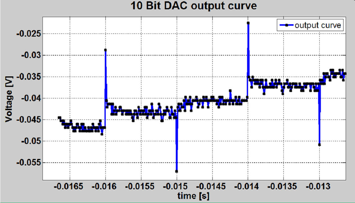
This example zooms around 1.5V in the combined graph. Combining measurements is difficult to have no gaps and no overlap between measurements to allow correct DNL and INL calculation.
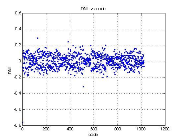
The DNL shows a nice random distribution below 0.5 LSB.
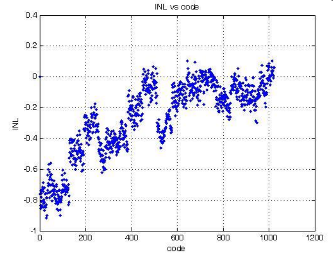
The INL starts with -0.8 LSB and ends with 0 LSB. It should start at 0 LSB.
Jumps can be seen in INL which are also single high points in DNL graph.
These jumps can be either attributed to errors in the DAC because of resistance value tolerance or due to measurement errors when changing trigger, offset and range at the oscilloscope.
Resistance value tolerance will show up at transitions of 511/512, 255/256 and 767/768 and so on.
An steady increase or decrease of INL is due to errors in LSB value or accuracy.
Solution:
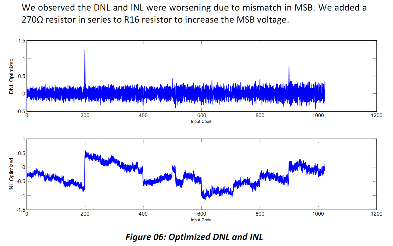
If there is a step which is to low or to high, small series resistance can be added.
Normally this happens first at the MSB.
Solution:
Solution:
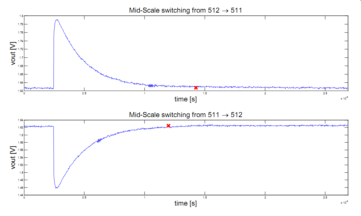
The settling time is measured for full scale and mid level transitions:
000 -> 3FF
3FF -> 000
1FF -> 200
200 -> 1FF
Settling times are measured until the output signals stays inside the 1/2 LSB bound error.
The full scale settling time should be approximated by measuring the time t1 reaching 50% level and applying the equation:
\( t_{settling} = (B+1) \cdot t_1 \)
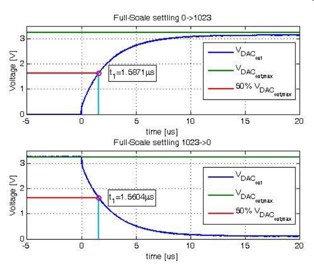
Typical values for setttling times are:
20 µ ..500 µs
Maximum frequency is therefore:
2 kHz .. 50 kHz
Comparing measurements using 1/2 LSB error for full level with approximation by using 50% range, show that the approximation underestimates settling times by a factor of 10.
Measure with different frequencies and input voltage ranges.
Exchange 2 data lines and measure the impact.
Solution:
A FFT needs a power of 2 number of samples. With the Electronic Explorer 16 k samples are possible.
A prime number of input periods should be present during this time to prevent bleeding.
Since the Electronic Explorer has a 10 Bit ADC the signal to noise ratio will be less than \( SNR = 10 \cdot 6.02 dB + 1.76 dB = 62 dB \)
Estimations of level on a log or dB scale are difficult, since peaks contribute a lot more to the total noise level.
The number of FFT points NFFT distributes noise and reduces the noise level by:
\( 10 \cdot log\frac{N_{FFT}}{2} \)
16 k samples will reduce the noise level by 40 dB.
To avoid distortion each sampling point from the oscilloscope should take a maximum of one output sample.
Otherwise a sawtooth signal is added to the sine signal and harmonics will occur.
A typical oscilloscope picture of a student group is shown:
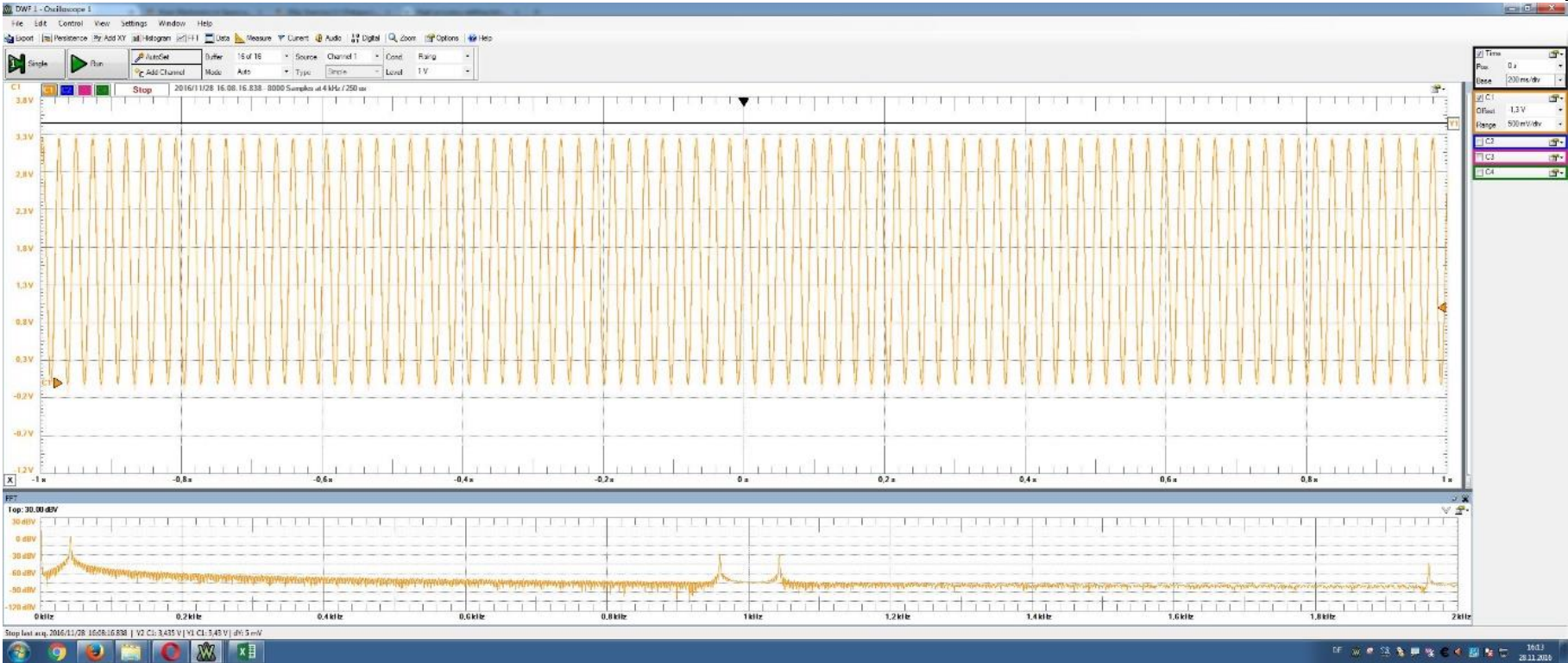
Measurement time 2s, 80.x periods (Bleeding), oscilloscope sampling time: 2s/16k = 62 us, Pattern frequency 1kHz is 1ms per sample.
An osciloscope picture of a correct measurement is shown here:
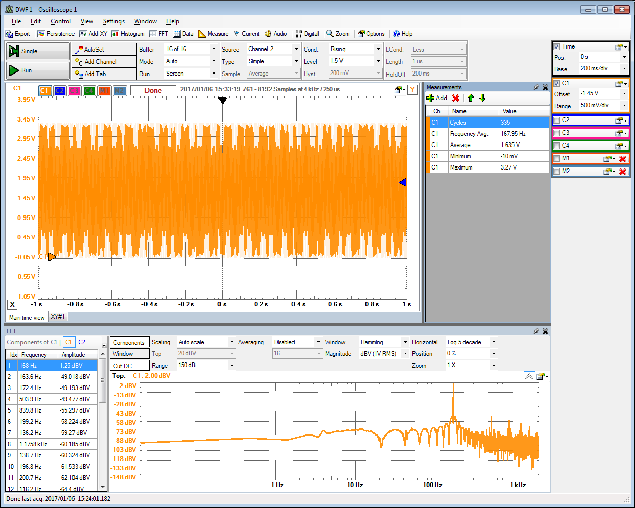
The FFT window allows to show the 'Components', the magnitude of biggest frequency components. It can show the 'Window' to suppress bleeding and can 'Cut DC'.
Every 250us a sample is generated by the pattern generator and taken by the oscilloscope.
There is no bleeding visible. The signal has an amplitude of 1.25dBV.
The first harmonic has -49.018 dBV.
Unfortunately the total noise level is not calculated.
Therefore the time data are exported ('Main Window' Copy to clipboard) and converted to positive integer numbers round(16k * Vout) + 135 and filled into the web page:
FFT Javascript
After 'Read integer data' and 'Generate Charts' the following graphs and numbers are available:
Signal to Noise
| Frequency | signal magnitude dB | Total noise magnitude dB |
| 344 | 82.53 | 34.51 |
| 1032 | 31.84 | 31.14 |
| 1720 | 26.05 | 29.53 |
| 2408 | 21.14 | 28.84 |
| 280 | 16.48 | 28.58 |
| 3096 | 16.39 | 28.31 |
| 408 | 16.37 | 28.03 |
| 968 | 13.63 | 27.87 |
| 1784 | 13.45 | 27.71 |
| 904 | 12.72 | 27.57 |
| 1656 | 12.46 | 27.43 |
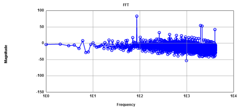
The signal to noise ratio is 82.53 dB - 34.51 dB = 48 dB. This is 48 dB / 6.07 dB = 8 Bit.
Removing the next 3 harmonics would reduce the noise level to 28.84 dB giving nearly one Bit more.
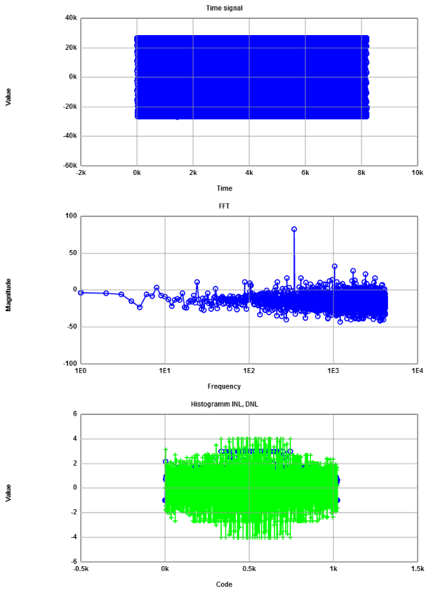
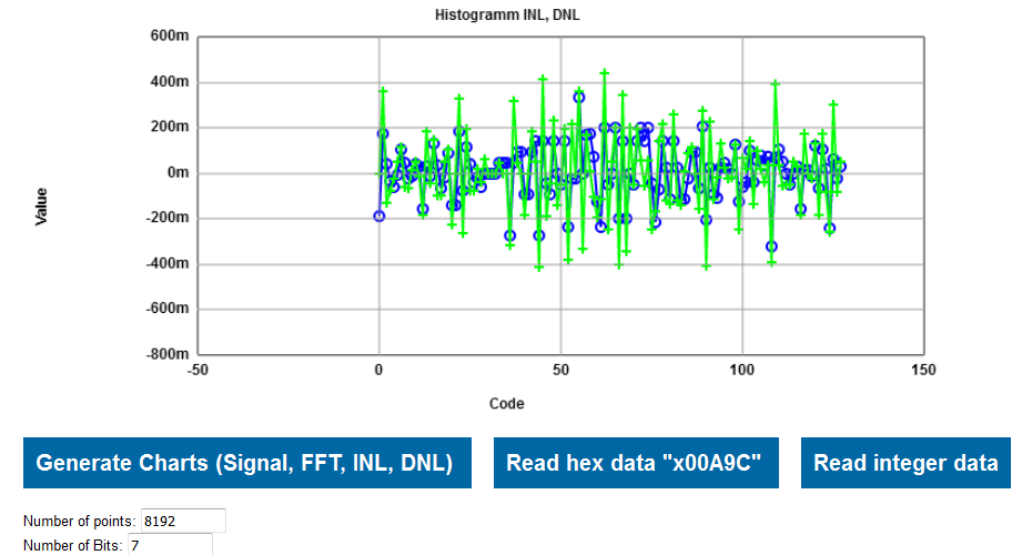
The INL, DNL charts show variations of up to 4 LSBs for a 10 Bit ADC bringing ENOB down to 8 Bit.
It is possible at the web page to reduce the number of Bits to 7 (rounding) giving an INL and DNL below 0.5.
Investigation of a 1kHz pattern generator signal shows the following FFT.
Each value of the pattern generator is sampled 4 times by the oscilloscope.
Signal to Noise
| Frequency | signal magnitude dB | Total noise magnitude dB |
| 86 | 82.57 | 56.52 |
| 1962 | 53.82 | 53.18 |
| 2134 | 52.75 | 42.97 |
| 4010 | 42.02 | 35.92 |
| 258 | 32.12 | 33.58 |
| 430 | 26.95 | 32.51 |
| 602 | 24.19 | 31.82 |
| 774 | 22.53 | 31.28 |
| 946 | 19.1 | 31.01 |
| 102 | 17.93 | 30.79 |
| 1274 | 17.8 | 30.56 |
Solution and Outlook
This laboratory showed challenges measuring DACs, while proving to be able to build a 8 Bit DAC.
The first real experience was to determine necessary accuracy for minimum, maximum and step size.
The second real experience was the effort to measure all codes of an DAC.
The third real experience lay in the FTT analysis to determine the right number of samples, sampling time and pattern generator frequency and synchronization. Calculating a correct noise level was also very dificult.
It is planned to use a band-stop filter to suppress the original signal and to be able to get a good estimate of the noise level.
In the next laboratory a sigma delta modulator is built and used to measure accuracy, INL, DNL and signal to noise ratio.
It is then difficult to determine whether errors are coming fromn the DAC or ADC.