Interface ElectronicsLaboratory 05: Pipeline ADCProf. Jörg Vollrath |
Overview
- Circuit
- LTSPICE simulation: Ramp, sine
- FFT, INL, DNL, SNR
- Summary
This is a laboratory to simulate (, build and measure) a pipeline ADC.
Pipeline ADC circuit: Overview
- Simulate a ramp signal with static CLKs and discuss the transfer characteristic.
Comment out the .save command to see all signals.
Deactivate the CLK PULSE statements and activate the static CLK DC statements.
Ramp or sine signal is selected by switching the node name form INX to IN in the respective statements.
Removing and inserting semicolons ; activates one or the other option.
Generating a positiv digital signal Dout from 0V to 3V requires R3 and R4 connected to VDDp.
On the left are the 2 switches selecting input voltage V(in) (CLK1) or V(res) (CLK3) from a pipeline stage operation.
The voltage Vin is saved as Vinx on sample and hold capacitor C1.
The comparator X3 generates data output Dout.
Vout = 2 * Vinx - Dout is generated by X1 and saved via a switch on C2 (CLK2) as Voutx. Buffer X6 feeds VoutX as residue Vres back to the input for the next cycle.
CLK 1 is shortly activated to sample V(in) and generate the first Dout. For the number of required bits CLK2 and then CLK 3 is activated generating the remaining bits.
V3 INX 0 PULSE(-1.5 1.8 0 983.4m 983.4m 0 1966.8m)
V5 IN 0 SINE(0.181 1.521 19.32779948)
This simulation contains static CLK for simulating transfer characteristic.
VCLK1 CLK1 0 PULSE(-3 3 5u 100n 100n 19.9u 480u)
VCLK2 CLK2 0 PULSE(-3 3 30u 100n 100n 19.9u 60u)
VCLK3 CLK3 0 PULSE(-3 3 55u 100n 100n 19.9u 60u)
;VCLK1 CLK1 0 DC 3
;VCLK2 CLK2 0 DC 3
;VCLK3 CLK3 0 DC 0
Dynamic CLK statements (PULSE) are used for normal operation generating serially 8 bit at Dout.
Removing and inserting semicolons ; activates one or the other option.
Generating a positiv digital signal Dout from 0V to 3V requires R3 and R4 connected to VDDp.
On the left are the 2 switches selecting input voltage V(in) (CLK1) or V(res) (CLK3) from a pipeline stage operation.
The voltage Vin is saved as Vinx on sample and hold capacitor C1.
The comparator X3 generates data output Dout.
Vout = 2 * Vinx - Dout is generated by X1 and saved via a switch on C2 (CLK2) as Voutx. Buffer X6 feeds VoutX as residue Vres back to the input for the next cycle.
CLK 1 is shortly activated to sample V(in) and generate the first Dout. For the number of required bits CLK2 and then CLK 3 is activated generating the remaining bits.
Dynamic ramp simulation
- Simulate a ramp signal with CLK operation and calculate INL and DNL.
Save the LTSPICE raw file under C:\temp\raw.
Activate the .save command.
Activate the CLK PULSE statements and deactivate the static CLK DC statements.
What is the sample frequency?
What is the input range?
What is the output range of Vouty?
Extract data with Read Raw File. - Use the ramp signal for calibration
- How do CLK1, CLK2 and CLK3 control operation?
How many bits are generated? - How many samples are simulated?
- What is the resolution of INL, DNL calculation with this number of samples?
- What is the Vmax and LSB of the DAC?
- Optimize the simulation and extract INL and DNL
Dynamic sine simulation
- Simulate a sine signal with CLK operation and calculate INL and DNL.
Activate the .save command.
Activate the CLK PULSE statements and deactivate the static CLK DC statements.
Adjust the range of the sine signal to generate all codes?
What is the input range?
What is the output range of Vouty?
Extract data with Read Raw File . - Use the ramp signal for calibration
- Simulate a sine signal and calculate SNR, ENOB
- What are the optimum values for extraction and calculation?
- Simulate a sine signal and calculate SNR, ENOB with calibration
- How many samples are simulated?
- Is there a difference in INL and DNL between ramp and sine measurement?
What improvements could you apply to the circuit?
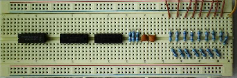
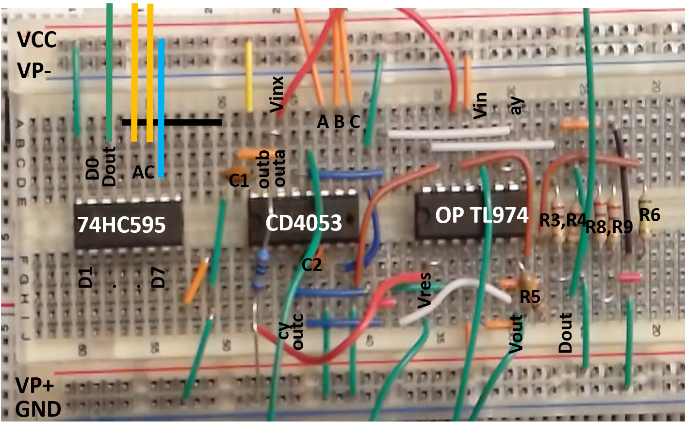
Building the circuit
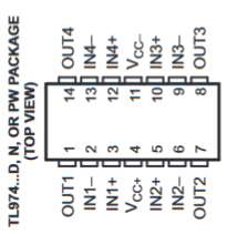
- Opamps in the schematic are realized with TL974
- Sample and hold with switches are realized with CD4053
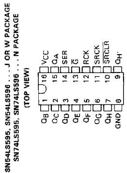
- Serial parallel conversion is done using a SN74HC595
- Since many connections are needed a step by step approach will be used.
- Opamp buffer characterization
- Sample and hold switch characterization
- Comparator measurement
- Residue generation
- Second sample and hold
- Closing the loop
- Shift register

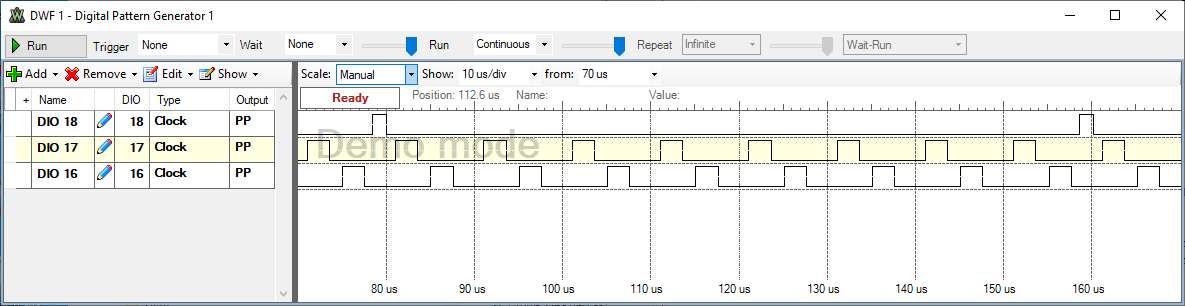
DIO18: CLK1 A; fsample, up time: 1/50 Tsample, delay: 0
DIO17: CLK2 C; 8*fsample, up time: 1/4 Tsample, phase: 234°
DIO16: CLK3 B; 8*fsample, up time: 1/4 Tsample, phase: 90°
tswitch active = 1µs; works with relaxed Tswitch = 10 µs
fswitch1 = 12.5 kHz; Duty 2%; Phase 0 deg;
fswitch2 = 100 kHz; Duty 25%; Phase 234 deg;
fswitch3 = 100 kHz; Duty 25%; Phase 90 deg;
Input buffer Opamp
Measure with the oscilloscope minimum and maximum output voltage, gain, bandwidth and slew rate limit.
Distribute VCC, VP-, VP+ and GND along the orange and blue lines on the bread board.
Apply VP+ = 3 V, VP- = -3V, VCC = 3.3 V via the 'Voltage' control panel.
Apply a sine or rectangular waveform to the input using the 'WaveGen' control panel.
Maximum input level:
Minimum input level:
Maximum slew rate:
Maximum bandwidth:
Is the maximum frequency limited by slew rate or bandwidth?
Connections:
Apply: VP+ 3V, VP- 3V, AWG1 sine, 0V offset, xx V amplitude
This is the last step for WS2019 to be completed.
Make a report as a web page.
Send a ziped group directory with your data containing also a printout of the webpage in a pdf file to joerg.vollrath@hs-kempten.de.
You can use the freeware program PDF Creator for generating the pdf file.
The directory should be named 2019_Group<X>00 with your group <X>.
Each question should be answered. The answer should be correct/make sense. There should be some text discussing the work strategy, obstacles and results. Submission should happen until 2.2.2020. A nice document format and correct use of English language and spelling is graded.
Apply VP+ = 3 V, VP- = -3V, VCC = 3.3 V via the 'Voltage' control panel.
Apply a sine or rectangular waveform to the input using the 'WaveGen' control panel.
Maximum input level:
Minimum input level:
Maximum slew rate:
Maximum bandwidth:
Is the maximum frequency limited by slew rate or bandwidth?
Connections:
| Net name | IC | pinNr | IC | pinNr |
| VP+ | TL974 | 4 | EE | VP+ |
| VP- | TL974 | 11 | EE | VP- |
| vin | TL974 IN3+ | 10 | EE | AWG1 |
| vin | EE | OSC1 | EE | AWG1 |
| vin1 | TL974 IN3- | 9 | TL974 OUT3 | 8 |
| vin1 | TL974 OUT3 | 8 | EE | OSC2 |
Apply: VP+ 3V, VP- 3V, AWG1 sine, 0V offset, xx V amplitude
Laboratory finish
This is the last step for WS2019 to be completed.
Report
Make a report as a web page.
Send a ziped group directory with your data containing also a printout of the webpage in a pdf file to joerg.vollrath@hs-kempten.de.
You can use the freeware program PDF Creator for generating the pdf file.
The directory should be named 2019_Group<X>00 with your group <X>.
Grading:
Each question should be answered. The answer should be correct/make sense. There should be some text discussing the work strategy, obstacles and results. Submission should happen until 2.2.2020. A nice document format and correct use of English language and spelling is graded.
Sample and hold
Measure with the oscilloscope limits of the sample and hold.What sine frequency and amplitude do you need?
What clock frequency do you need for CLK1 for the switch?
Distribute VCC, VP-, VP+ and GND along the orange and blue lines on the bread board.
Added Connections:
Apply: VP+ 3V, VP- 3V, AWG1 sine, 0V offset, xx V amplitude
Generate a clock with DIO18
Added Connections:
| Net name | IC | pinNr | IC | pinNr |
| VSS | CD4053 VSS | 8 | EE | GND |
| VCC | CD4053 VDD | 16 | EE | VCC |
| vin1 | CD4053 ay | 16 | TL974 | 8 |
| CLK1 | CD4053 Sel A | 11 | EE | DIO18 |
| vinx | CD4053 OUT a | 14 | EE | OSC3 |
| GND | CD4053 INH | 6 | EE | GND |
| VP- | CD4053 VEE | 7 | EE | VP- |
| VINX | C1 | 1 | CD4053 OUT a | 14 |
| GND | C1 | 2 | EE | GND |
Apply: VP+ 3V, VP- 3V, AWG1 sine, 0V offset, xx V amplitude
Generate a clock with DIO18
Comparator
Document the transfer characteristic.
Added Connections:
Added Connections:
| Net name | IC | pinNr | IC | pinNr |
| Vinx | TLC974 IN4+ | 12 | Cd4053 OUTA | 14 |
| Vref1 | TLC974 IN4- | 13 | EE | Vref1(GND) |
| Dx | TLC974 OUT4 | 14 | R3 | 1 |
| Dout | R3 | 2 | R4 | 1 |
| VDDp | R4 | 2 | EE | VP+ |
| Dx | TLC974 OUT4 | 14 | R8 | 1 |
| Dy | R8 | 2 | R6 | 1 |
| Dy | R8 | 2 | R9 | 1 |
| GND | R9 | 2 | EE | GND |
| R6 | 2 | R5 | 1 | |
| R6 | 2 | TLC974 IN2- | 6 | |
| Vout | R5 | 2 | TLC974 OUT2 | 7 |
| Vinx | CD4053 OUTA | 14 | TLC974 IN2+ | 5 |
Residue
Added Connections:
| Net name | IC | pinNr | IC | pinNr |
| Vout | TLC974 OUT2 | 7 | CD4053 CY | 3 |
| CLK2 | CD4053 C | 9 | EE | DIO17 |
| Voutx | CD4053 OUTC | 4 | TLC974 IN1+ | 3 |
| Voutx | CD4053 OUTC | 4 | C2 | 1 |
| GND | C2 | 2 | EE | GND |
| Vres | TLC974 OUT1 | 1 | TLC974 IN1- | 2 |
Finish
Added Connections closing the loop:
| Net name | IC | pinNr | IC | pinNr |
| Vres | TLC974 OUT1 | 1 | CD4053 BY | 1 |
| CLK3 | CD4053 B | 10 | EE | DIO16 |
| Vinx | CD4053 OUTB | 15 | TLC974 IN4+ | 12 |
Serial parallel:
| Net name | IC | pinNr | IC | pinNr |
| Dout | R3 | 2 | SN74HC595 SER | 14 |
| D0 | SN74HC595 D0 | 15 | EE | DIO8 |
| D1 | SN74HC595 D1 | 1 | EE | DIO9 |
| D2 | SN74HC595 D2 | 2 | EE | DIO10 |
| D3 | SN74HC595 D3 | 3 | EE | DIO11 |
| D4 | SN74HC595 D4 | 4 | EE | DIO12 |
| D5 | SN74HC595 D5 | 5 | EE | DIO13 |
| D6 | SN74HC595 D6 | 6 | EE | DIO14 |
| D7 | SN74HC595 D7 | 7 | EE | DIO15 |
| GND | SN74HC595 GND | 8 | EE | GND |
| VCC | SN74HC595 /SRCLR | 10 | EE | VCC |
| C | SN74HC595 SRCK | 11 | EE | DIO17 |
| A | SN74HC595 RCK | 12 | EE | VCC |
| VCC | SN74HC595 VCC | 16 | EE | VCC |
| SN74HC595 /G | 13 |