Pipeline ADC circuit: Overview
- Simulate a ramp signal with static CLKs and discuss the transfer characteristic.
Comment out the .save command to see all signals.
Deactivate the CLK PULSE statements and activate the static CLK DC statements.
Ramp or sine signal is selected by switching the node name form INX to IN in the respective statements.
Removing and inserting semicolons ; activates one or the other option.
Generating a positiv digital signal Dout from 0V to 3V requires R3 and R4 connected to VDDp.
On the left are the 2 switches selecting input voltage V(in) (CLK1) or V(res) (CLK3) from a pipeline stage operation.
The voltage Vin is saved as Vinx on sample and hold capacitor C1.
The comparator X3 generates data output Dout.
Vout = 2 * Vinx - Dout is generated by X1 and saved via a switch on C2 (CLK2) as Voutx. Buffer X6 feeds VoutX as residue Vres back to the input for the next cycle.
CLK 1 is shortly activated to sample V(in) and generate the first Dout. For the number of required bits CLK2 and then CLK 3 is activated generating the remaining bits.
There was an error for static measurement: VCLK3 DC has to be -3 V instead of 0 V to turn the switch off.
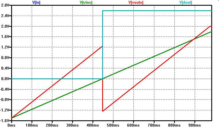
Figure: Static residue curve for the pipeline ADC
A dout signal 0V..2.6V is generated.
Input range for static simulation is from -1.4495 V up to 1.50 V.
These are the crossing points of V(voutx) = V(vinx).
There will be missing codes due to output voltages V(voutx) at the switching point of:
1.2444 V; -1.2444 V.
1.2444 V/ 1.5 V = 0.83 = 83%
Missing codes are expected.
The simulation time is .
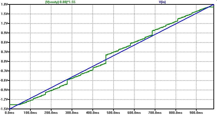
Figure: Dynamic ramp for the pipeline ADC
Simulation took 38 minuntes with maximum timestep 10u and all signals saved.
To extract input range V(vouty) was scaled (V(vouty)-0.88)*1.55 to be close to the V(in) range.
Input range -1.35 V..1.71 V
The input range is shifted compared to static simulation, probably due to some switch coupling.
For optimum data extraction the start and stop time of the ramp are measured: 43ms..958.9ms.
V3 INX 0 PULSE(-1.5 1.8 0 983.4m 983.4m 0 1966.8m)
V5 IN 0 SINE(0.181 1.521 19.32779948)
This simulation contains static CLK for simulating transfer characteristic.
VCLK1 CLK1 0 PULSE(-3 3 5u 100n 100n 19.9u 480u)
VCLK2 CLK2 0 PULSE(-3 3 30u 100n 100n 19.9u 60u)
VCLK3 CLK3 0 PULSE(-3 3 55u 100n 100n 19.9u 60u)
;VCLK1 CLK1 0 DC 3
;VCLK2 CLK2 0 DC 3
;VCLK3 CLK3 0 DC -3
Dynamic CLK statements (PULSE) are used for normal operation generating serially 8 bit at Dout.
Removing and inserting semicolons ; activates one or the other option.
Generating a positiv digital signal Dout from 0V to 3V requires R3 and R4 connected to VDDp.
On the left are the 2 switches selecting input voltage V(in) (CLK1) or V(res) (CLK3) from a pipeline stage operation.
The voltage Vin is saved as Vinx on sample and hold capacitor C1.
The comparator X3 generates data output Dout.
Vout = 2 * Vinx - Dout is generated by X1 and saved via a switch on C2 (CLK2) as Voutx. Buffer X6 feeds VoutX as residue Vres back to the input for the next cycle.
CLK 1 is shortly activated to sample V(in) and generate the first Dout. For the number of required bits CLK2 and then CLK 3 is activated generating the remaining bits.
Solution:
Static CLK residue ramp measurement
There was an error for static measurement: VCLK3 DC has to be -3 V instead of 0 V to turn the switch off.
Figure: Static residue curve for the pipeline ADC
A dout signal 0V..2.6V is generated.
Input range for static simulation is from -1.4495 V up to 1.50 V.
These are the crossing points of V(voutx) = V(vinx).
There will be missing codes due to output voltages V(voutx) at the switching point of:
1.2444 V; -1.2444 V.
1.2444 V/ 1.5 V = 0.83 = 83%
Missing codes are expected.
Dynamic CLK ramp measurement
The simulation time is .
Figure: Dynamic ramp for the pipeline ADC
Simulation took 38 minuntes with maximum timestep 10u and all signals saved.
To extract input range V(vouty) was scaled (V(vouty)-0.88)*1.55 to be close to the V(in) range.
Input range -1.35 V..1.71 V
The input range is shifted compared to static simulation, probably due to some switch coupling.
For optimum data extraction the start and stop time of the ramp are measured: 43ms..958.9ms.
Dynamic ramp simulation
- Simulate a ramp signal with CLK operation and calculate INL and DNL.
Save the LTSPICE raw file under C:\temp\raw.
Activate the .save command.
Activate the CLK PULSE statements and deactivate the static CLK DC statements.
What is the sample frequency?
What is the input range?
What is the output range of Vouty?
Extract data with Read Raw File. - Use the ramp signal for calibration
- How do CLK1, CLK2 and CLK3 control operation?
How many bits are generated? - How many samples are simulated?
- What is the resolution of INL, DNL calculation with this number of samples?
- What is the Vmax and LSB of the DAC?
- Optimize the simulation and extract INL and DNL
Solution
Every TCLK1 = 480 µs CLK1 is activated for 20 µs to sample V(in).
Sample frequency is 1/TCLK1 = 2083 Hz.
The number of samples in the input range is (958.9ms-43ms)/0.48ms = 1908
The total number of samples are 983.4ms/0.48ms = 2049
Input range -1.35 V..1.71 V
A sine signal needs an offset of (1.71 V - 1.35 V)/2 = 0.18 V and an amplitude of (1.71 V - (-1.35 V))/2 = 1.53 V.
V(Vouty) is between 0 V and 2 V.
CLK2 and CLK3 run at 8 times the frequency of CLK1.
CLK1 samples external voltage v(in). CLK2 samples the residue on C2.
CLK3 transfers the residue back to the input sample and hold C1.
Since this is done 8 times, 8 bits are generated.
Samples per code: 2048/256 = 8.
Expected resolution is 1/8 = 0.125 LSB
Vmax of the DAC is controled by the data input level of VDD = 2 V.
LSB = 2 V / 256 = 7.8 mV.
Simulation data extraction
The first output value of 0 V is not valid.
Read Raw File needs: Start time: 43E-3
Stop time: 959.9E-3
Time step: 480E-6
Map to integer scales the voltage values into a range: 255
Button: Map to integer
Button ADC histogram ramp analysis.
This shows 84 missing codes.
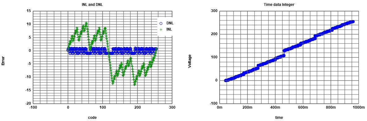
Figure: INL and DNL result of read raw.
This raw curve shows maximum absolute value of INL of 13.
4 bits will be lost.
The extracted integer data is here: Ramp data
This data can be used later for the FFT Analysis with calibration.
Here is the resulting code calibration lookup table: Code calibration lookup table
Missing codes will map to the next lower code.
The maximum code after lookup will be 171.
Here is the resulting code and slope calibration lookup table: Code and slope calibration lookup table
Missing codes will map to the next lower code.
The maximum code after lookup will be 127.
Dynamic sine simulation
- Simulate a sine signal with CLK operation and calculate INL and DNL.
Activate the .save command.
Activate the CLK PULSE statements and deactivate the static CLK DC statements.
Adjust the range of the sine signal to generate all codes?
What is the input range?
What is the output range of Vouty?
Extract data with Read Raw File . - Use the ramp signal for calibration
- Simulate a sine signal and calculate SNR, ENOB
- What are the optimum values for extraction and calculation?
- Simulate a sine signal and calculate SNR, ENOB with calibration
- How many samples are simulated?
- Is there a difference in INL and DNL between ramp and sine measurement?
What improvements could you apply to the circuit?
Solution
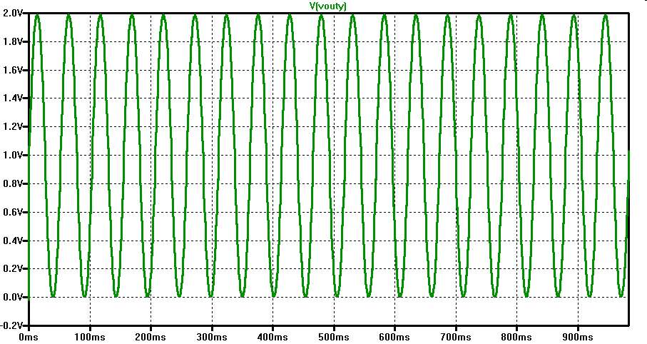
Figure: Digital sine signal.
Read Raw File
Start time: 480E-6
Stop time: 1
Time step: 480E-6
19 sine periods.
The extracted integer data is here: Sine data
This data is used for FFT Analysis.
Analysis is done with raw data, code calibrated data and slope calibrated data.
Code calibration eliminates unused codes. Since 85 codes are not used 171 codes remain.
Slope calibration looks for lowest slope and compensates for this: 127 codes remain.
Calibration updates the maximum number of occurences (MaxCount), noise limit (Bnoise) and minimum slope (Bslope) limit.
 |
 |
 |
| f = 19 asignal = 36.4 dB anoise = 10.4 dB | f = 19 asignal = 32.59 dB anoise = -10.79 dB | f = 19 asignal = 29.97 dB anoise = -11.77 dB |
| SNDR = 20 dB .. ENOB = 3.2 | SNDR = 43.38 dB .. ENOB = 7 | SNDR = 41.74 dB .. ENOB = 7 |
| MaxCount = 15, noise= 7.4, Bslope=7 | MaxCount = 26 noise= 7 Bslope= 6.2 |
Harmonics are damped with slope calibration, but no SNDR improvement can be seen.
There was a program bug. The time signal is scaled down from a range of 256 to 171 to 127 using code and slope calibration. This is not reflected in the INL, DNL graph.
Slope calibration seems not be effective for INL, DNL.
At the moment the maximum number of occurences for a code (MaxCount) is used for slope calibration. This results in an even higher number of occurences.
Since DNL could be up to 1 LSB perhaps a lower value down to MaxCount/2 could be used for improvement.
Automatic bucketing should be improved.
A better approach could be:
The codes with lowest occurence should be mapped to the next/previous lower code bucket.
Circuit improvements
GBW of Comparator was increased to 1GHz. This prevented any slope reversal in codes as pictured below.

Figure: Slow comparator signal V(dy)at 686.0ms causing bad output code at 686.4ms.
For a ramp only increasing codes should happen. At 686.4ms the code V(vouty) is one less than the cycles before.
R5 is 120k causing a lot of missing codes. This could be decreased to 105k to get less missing codes, but giving still some resilence to offset and gain error.
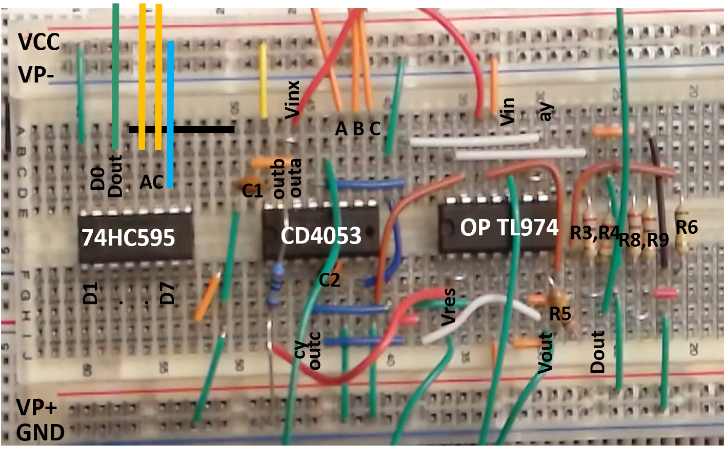
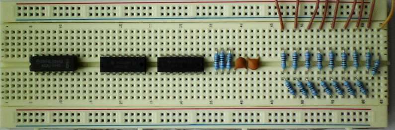
Building the circuit
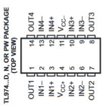
- Opamps in the schematic are realized with TL974
- Sample and hold with switches are realized with CD4053
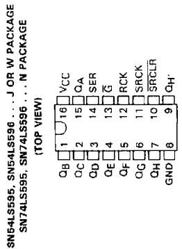
- Serial parallel conversion is done using a SN74HC595
- Since many connections are needed a step by step approach will be used.
- Opamp buffer characterization
- Sample and hold switch characterization
- Comparator measurement
- Residue generation
- Second sample and hold
- Closing the loop
- Shift register

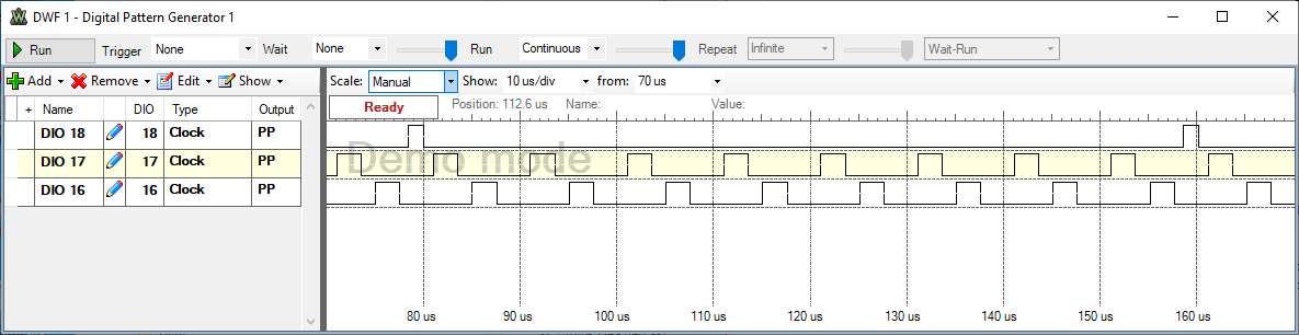
DIO18: CLK1 A; fsample, up time: 1/50 Tsample, delay: 0
DIO17: CLK2 C; 8*fsample, up time: 1/4 Tsample, phase: 234°
DIO16: CLK3 B; 8*fsample, up time: 1/4 Tsample, phase: 90°
tswitch active = 1µs; works with relaxed Tswitch = 10 µs
fswitch1 = 12.5 kHz; Duty 2%; Phase 0 deg;
fswitch2 = 100 kHz; Duty 25%; Phase 234 deg;
fswitch3 = 100 kHz; Duty 25%; Phase 90 deg;
Residue
Added Connections:
| Net name | IC | pinNr | IC | pinNr |
| Vout | TLC974 OUT2 | 7 | CD4053 CY | 3 |
| CLK2 | CD4053 C | 9 | EE | DIO17 |
| Voutx | CD4053 OUTC | 4 | TLC974 IN1+ | 3 |
| Voutx | CD4053 OUTC | 4 | C2 | 1 |
| GND | C2 | 2 | EE | GND |
| Vres | TLC974 OUT1 | 1 | TLC974 IN1- | 2 |