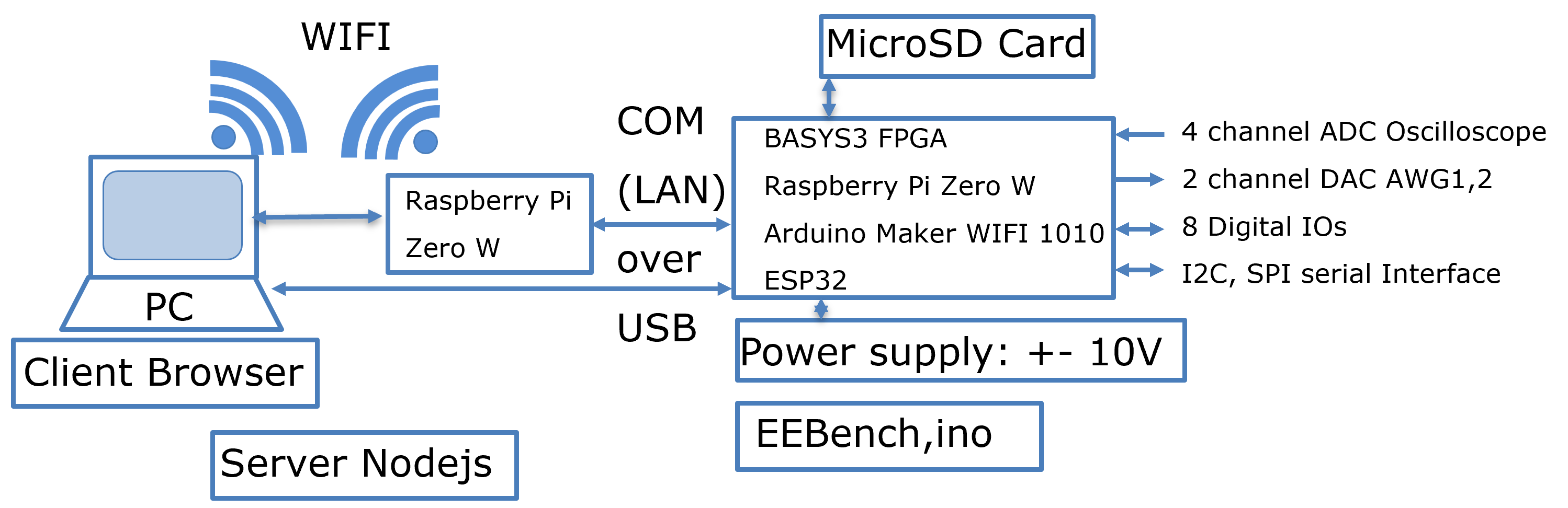
Platform Hardware
|
Arduino MKR WIFI 1010 (BASYS3, Rpi) Breadboard, PMOD DA2, AD2 8-Bit R2R DAC Cardboard Box Options for projects: (C serial DAC, Scalable R2R DAC, Interpolating DAC, R-String (SAR ADC, pipeline ADC) |
  |
Platform Software PC
Data Converter CharacterizationServer NodeJS: StartServerAx.bat ServerAx.js User Interface: Browser: Projekte/SerialA.html Arduino: Arduino/DataConverterCharV4/DataConverterCharV4.ino NodeEEBenchServer NodeJS: NodeEEBench.bat ServerEEBench.js User Interface: Browser: Projekte/NEEBench.html Arduino: Arduino/EEBench/EEBench.ino |
|
Installation Instructions
The 'Data Converter Characterization' software is optimized for INL, DNL ramp
measurement, lookup table transsfer and FFT. There are only limited options
for waveforms and codes are displayed at the Oscilloscope window.
The 'NodeEEBench' software is more general and not yet fully functional for INL, DNL ramp measurement, lookup table transfer and FFT.
Get a .zip file from the Github repository of NodeEEBench.
Github Repository NodeEEBench
Unzip the file to C:\temp.
Rename the directory C:\temp\NodeEEBench-master to C:\temp\NodeEEBench.
There should no subdirectory NodeEEBench-master in there, but all kind of files and also a directory Arduino in there.
(Optional: Continue with 'Check Current Installation with NodeEEBench'.)
Connect the Arduino MKR WIFI 1010 Board to the PC.
Configure the Arduino Board with the following sketch:
Directory: C;\temp\NodeEEBench\Arduino\DataConverterV4\DataConverterV4.ino
The IDE needs Tools, Board, Board Manager, Arduino SAMD Boards
The IDE needs Tools, Board, Boards, Arduino SAMD Boards, Arduino MKR WIFI 1010
The IDE needs Tools, Port: 'COM xx' for Arduino MKR WIFI 1010
Sketch, Upload
Start the server:
Directory: C;\temp\NodeEEBench
Start: StartServerAx.bat
A command line window opens.
A message about a webserver is displayed
'Sever running at http://localhost:3000'
If the Arduino is not detected the program will stop with an error message.
Check in the Arduino IDE that a connection to the Arduino board is detected.
Open an Internet Browser and go to the address http://localhost:3000.
At the end of your session please stop the nodejs server with a <STRG>C keyboard entry and close the command line window.
Before Installation of software check the current status.
Connect the Arduino MKR WIFI 1010 Board to the PC.
Configure the Arduino Board with the following sketch:
Directory: C;\temp\NodeEEBench\Arduino\NodeEEBench\NodeEEBench.ino
The IDE needs Tools, Board, Board Manager, Arduino SAMD Boards
The IDE needs Tools, Board, Boards, Arduino SAMD Boards, Arduino MKR WIFI 1010
The IDE needs Tools, Port: 'COM xx' for Arduino MKR WIFI 1010
Sketch, Upload
Start the server:
Directory: C;\temp\NodeEEBench
Start: NodeEEBench.bat
A command line window opens.
A message about a webserver is displayed
'Sever running at http://localhost:3000'
Open an Internet Browser and go to the address http://localhost:3000.
Check the Version of the software.
Old versions will not show a version number.
Check the detected configuration System Board: Arduino MKR Wifi 1010
Without the Arduino Board 'Simulation' will be activated.
At the end of your session please stop the nodejs server with a <STRG>C keyboard entry and close the command line window.
While the server is running the Arduino IDE can not access and program the Arduino.
Stop the server, upload the sketch, start the server with the batch file.
Make sure only one browser tab is connected to the server.
The 'NodeEEBench' software is more general and not yet fully functional for INL, DNL ramp measurement, lookup table transfer and FFT.
Installation
Get a .zip file from the Github repository of NodeEEBench.
Github Repository NodeEEBench
Unzip the file to C:\temp.
Rename the directory C:\temp\NodeEEBench-master to C:\temp\NodeEEBench.
There should no subdirectory NodeEEBench-master in there, but all kind of files and also a directory Arduino in there.
(Optional: Continue with 'Check Current Installation with NodeEEBench'.)
Starting Current Data Converter Characterization Installation
Connect the Arduino MKR WIFI 1010 Board to the PC.
Configure the Arduino Board with the following sketch:
Directory: C;\temp\NodeEEBench\Arduino\DataConverterV4\DataConverterV4.ino
The IDE needs Tools, Board, Board Manager, Arduino SAMD Boards
The IDE needs Tools, Board, Boards, Arduino SAMD Boards, Arduino MKR WIFI 1010
The IDE needs Tools, Port: 'COM xx' for Arduino MKR WIFI 1010
Sketch, Upload
Start the server:
Directory: C;\temp\NodeEEBench
Start: StartServerAx.bat
A command line window opens.
A message about a webserver is displayed
'Sever running at http://localhost:3000'
If the Arduino is not detected the program will stop with an error message.
Check in the Arduino IDE that a connection to the Arduino board is detected.
Open an Internet Browser and go to the address http://localhost:3000.
At the end of your session please stop the nodejs server with a <STRG>C keyboard entry and close the command line window.
Check Current Installation Status with NodeEEBench
Before Installation of software check the current status.
Connect the Arduino MKR WIFI 1010 Board to the PC.
Configure the Arduino Board with the following sketch:
Directory: C;\temp\NodeEEBench\Arduino\NodeEEBench\NodeEEBench.ino
The IDE needs Tools, Board, Board Manager, Arduino SAMD Boards
The IDE needs Tools, Board, Boards, Arduino SAMD Boards, Arduino MKR WIFI 1010
The IDE needs Tools, Port: 'COM xx' for Arduino MKR WIFI 1010
Sketch, Upload
Start the server:
Directory: C;\temp\NodeEEBench
Start: NodeEEBench.bat
A command line window opens.
A message about a webserver is displayed
'Sever running at http://localhost:3000'
Open an Internet Browser and go to the address http://localhost:3000.
Check the Version of the software.
Configuration (Version: NodeEEBenchV20251015.zip)
Note down the version and make a screen copy for your notes.Old versions will not show a version number.
Check the detected configuration System Board: Arduino MKR Wifi 1010
Without the Arduino Board 'Simulation' will be activated.
At the end of your session please stop the nodejs server with a <STRG>C keyboard entry and close the command line window.
Challenges
While the server is running the Arduino IDE can not access and program the Arduino.
Stop the server, upload the sketch, start the server with the batch file.
Make sure only one browser tab is connected to the server.
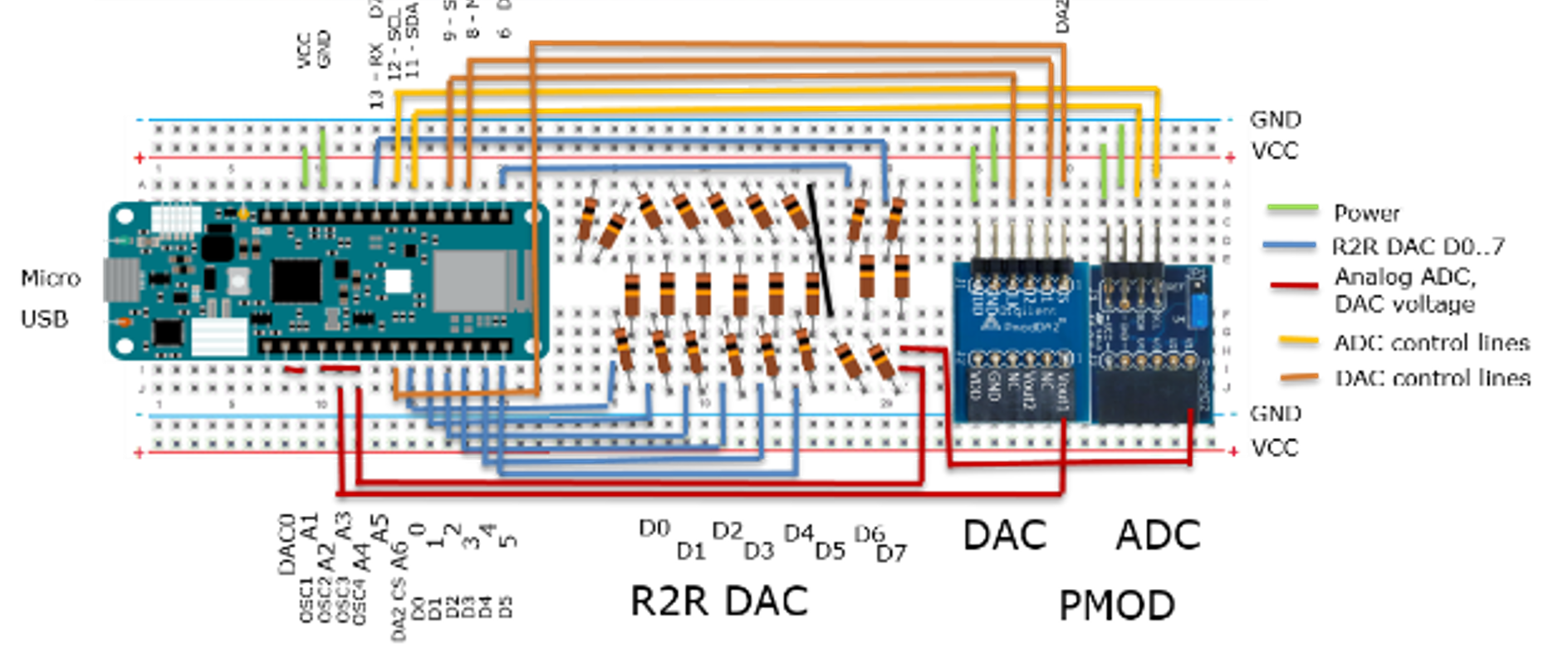
R2R Breadboard Circuit
|
DataConverterCharV4.ino AWG1: Original digital signal from generator C1: PMOD ADC C2: Arduino pin A1 C3: Arduino pin A2 C4: Arduino pin A3 Resistance can be added to the data lines D0..7 introducing error. |
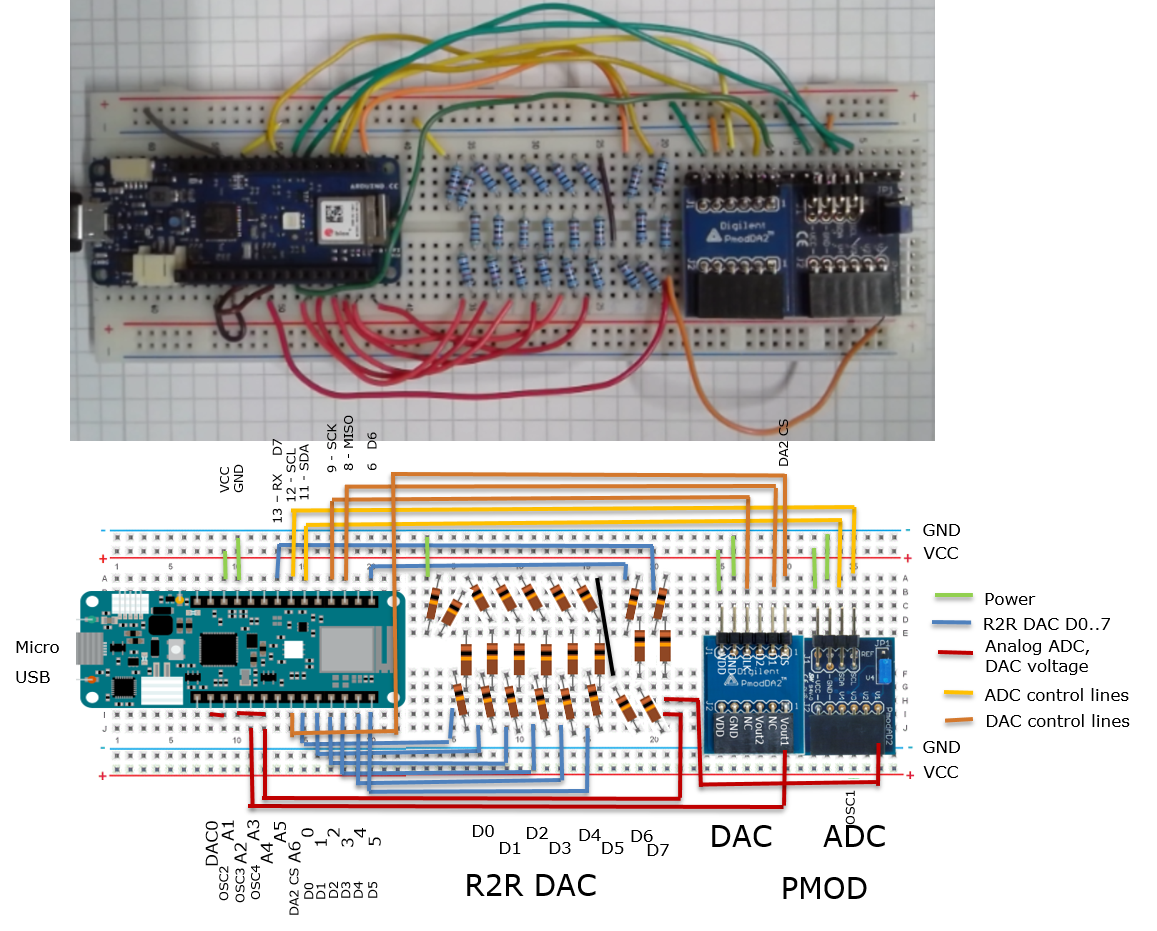 |
Wiring
R2R DAC
Build the R2R DAC on the board. Connect the output to OSC4, A4 and OSC2, A2, .
| Pin Arduino | Name | Name | R2R |
| D0 | D0 | D0 | D0 |
| D1 | D1 | D1 | D1 |
| D2 | D2 | D2 | D2 |
| D3 | D3 | D3 | D3 |
| D4 | D4 | D4 | D4 |
| D5 | D5 | D5 | D5 |
| D6 | D6 | D6 | D6 |
| D13 | D13 | D7 | D7 |
| A4 | OSC4 | Output R2R | Output R2R |
PMOD DA2 ( 2 Channel, 12-Bit, 125kHz, 8 µs)
Connect DA2 to the Arduino.

| Pin Arduino | Name | Name | Pin PMOD DA2 |
| D9 | SCK | CLK | 4 |
| D8 | MOSI | D1 | 2 |
| D21 | D21 | CS | 1 |
| GND | GND | GND | 5 |
| +3V3 | VCC | VDD | 6 |
Only Output Vout1 is used for signal generation.
Digilent: PMOD DA2 20.-
Texas Instruments DAC121S101 8us settling 12-Bit 16.5 MS/s $1.-
30 MHz SCLK
PMOD AD2
Connect AD2 to the Arduino.

| Pin Arduino | Name | Name | Pin PMOD AD2 |
| D12 | SCL | SCL | 1 |
| D11 | SDA | SDA | 2 |
| GND | GND | GND | 3 |
| +3V3 | VCC | VDD | 4 |
Only Input V1 is used for data acquisition.
Digilent: PMOD AD2 20.-
Analog devices AD7991 4 channel, I2C, 1us conversion time, 12-bit
Arduino Code (DataConverterCharV4.ino)
- Pin definition for R2R, PMOD AD2, PMOD DA2: '#define'
- PMOD DA2: void writeDAC(uint16_t sineValue)
- R2R DAC: void digWrite(uint16_t sineValue)
- PMOD AD2: int readADC(void)
void Init_AD7991(void)
           oscX = readADC();
           Serial.print(" , ADC(AD2) = ");
           Serial.print(oscX);
           oscX = analogRead(ADC_OSC1);
           Serial.print(" , ADC(OSC1) = ");
           Serial.print(oscX);
           oscX = analogRead(ADC_OSC2);
           Serial.print(" , ADC(OSC2) = ");
           Serial.print(oscX);
           oscX = analogRead(ADC_OSC3);
           Serial.print(" , ADC(OSC3) = ");
           Serial.print(oscX);
           oscX = analogRead(ADC_OSC4);
           Serial.print(" , ADC(OSC4) = ");
           Serial.print(oscX);
2024_Lab_MKRWIFI1010_R2R.html
Ramp and Sine Test
|
|
Video 13 Stromspiegel
|
Länge: 0:57:10 |
0:0:0 Laboratory Arduino R2R DAC
0:0:23 Overview
0:1:0 Hardware
0:2:40 User Interface StartServerAx.bat vs NodeEEBench.bat
0:3:53 Connect Arduino and look at it
0:5:30 Load Software from Github
0:6:40 Configure Arduino with sketch
0:8:40 StartServerAx.bat
0:10:11 Webinterface
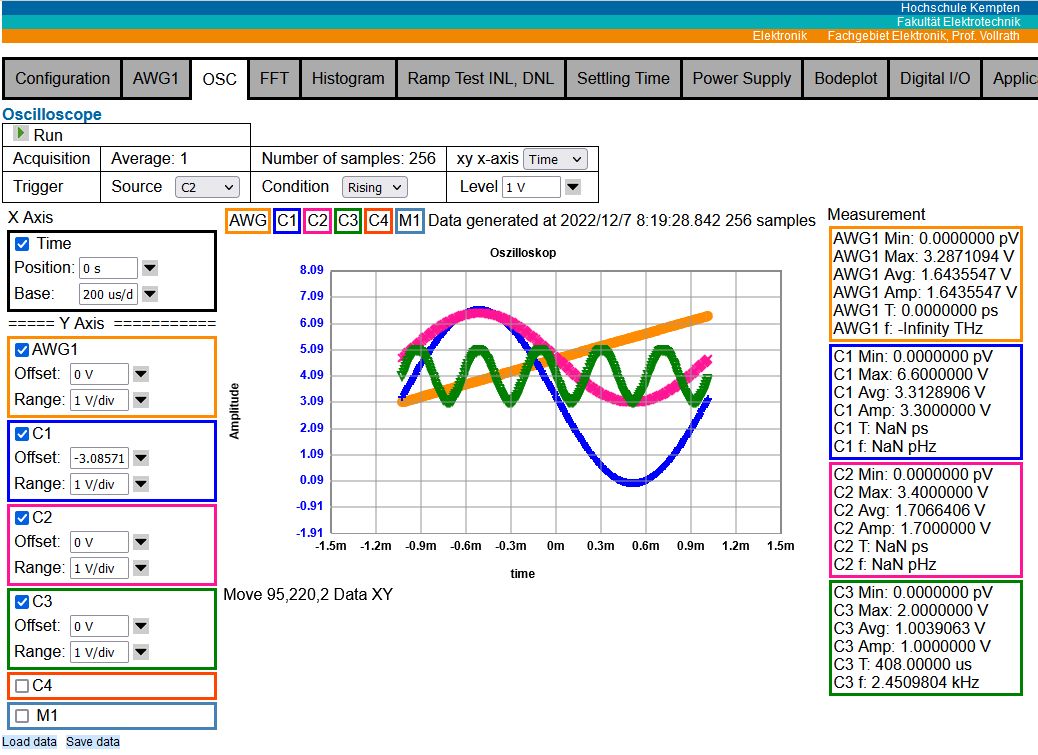
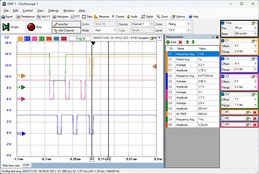
0:11:26 Oscilloscope picture ramp Electronic Explorer
0:13:20 Operate triangle
0:14:10 Start Oscilloscope from webinterface
0:15:18 Ramp test tab
0:19:40 Screenshot saved
0:21:10 Lookup table discussion
0:22:30 Sine signal
0:24:0 FFT analysis
0:25:40 AWG Signal to noise ratio and ENOB
0:27:0 C1 Signal to noise ratio and ENOB
0:29:0 C3 Signal to noise ratio and ENOB
0:30:55 Modified R2R D6 20k+4.7kOhm , D7 20k+2.2kOhm
0:32:20 Ramp test
0:33:30 Copy lookup table
0:34:0 New Sine
0:35:43 FFT SNR
0:37:0 Download Lookup table
0:38:30 Ramp with limited range
0:38:30 Limited sine signal
0:40:10 FFT SNR
0:41:34 Modified Arduino R2R DAC
0:42:1 Ramp
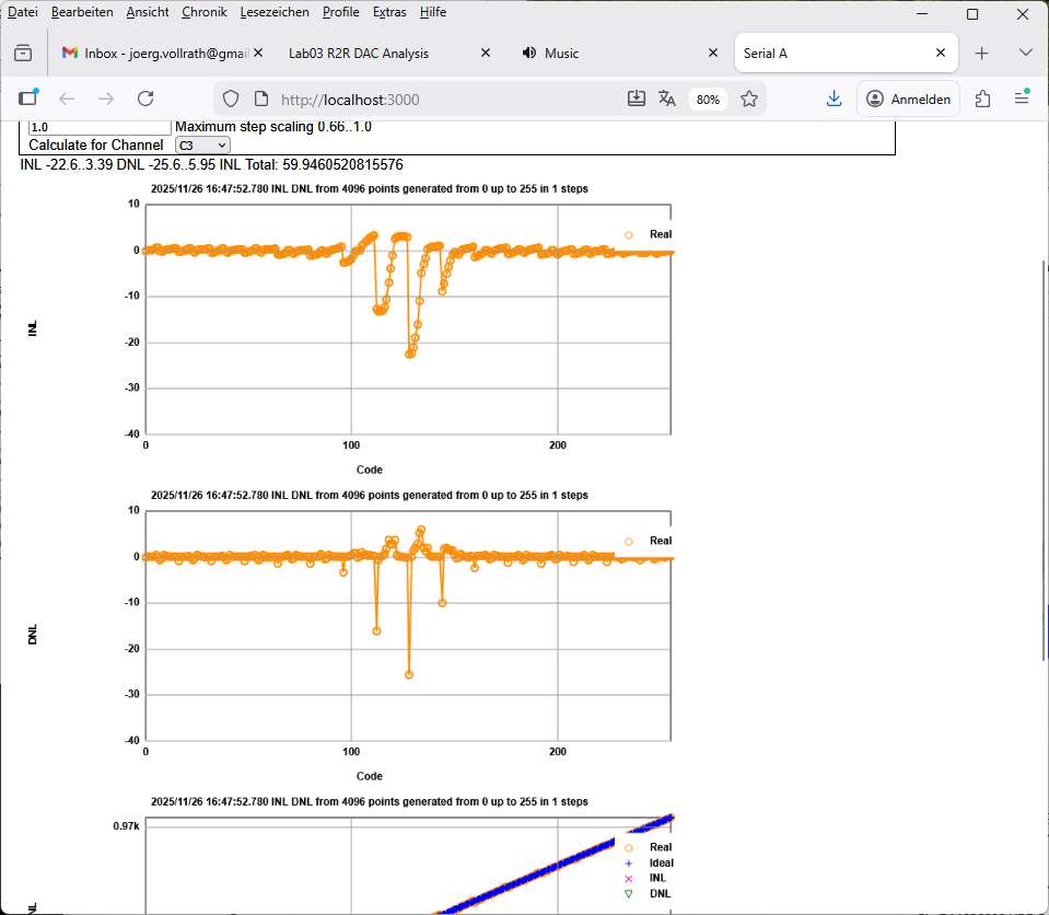
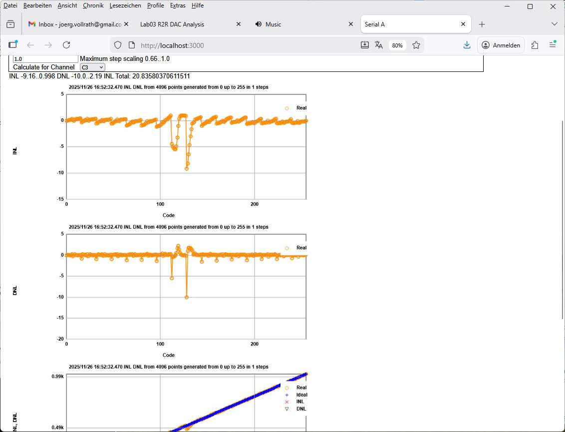
0:42:34 INL,DNL graph
0:43:14 Lookup table
0:44:29 Sine and FFT
0:45:4 FFT window SNR 30 dB, 5 Bits
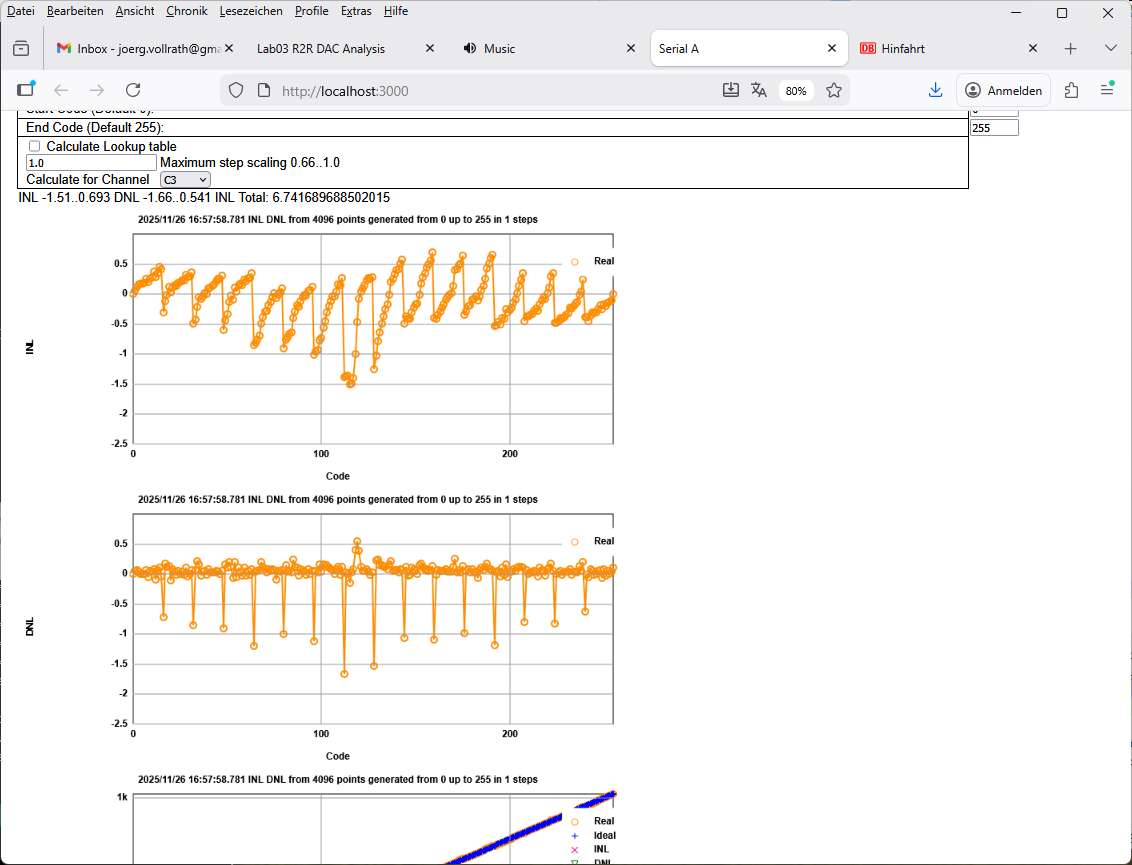
0:46:0 Lookup table 1.0
0:46:40 Ramp run
0:47:20 Range update INL, DNL
0:48:50 Lookup 0.9
0:49:42 INL, DNL up to 2.5
0:50:50 Lookup 1.1, ramp
0:51:40 INL, DNL result best
0:53:42 Sine signal
0:55:41 FFT SNR 44 dB, ENOB 7 Bit
0:57:10 Description
|
- Start Zoom full screen sharing
- Word file notebook
- Webcam Arduino Board connect to PC
- Directory C:\temp\NodeEEBench
- Arduino upload DataConverterCharV4.ino
- Start server: StartServerAx.bat
- Command window output
- Browser: user interface
- Activate Ramp: Observe Web interface
- INL, DNL Test
- Activate Sine signal
- FFT SNR
- Activate Ramp: Observe Web interface
- INL, DNL Test
- Download Lookup table
- Activate Sine signal
- FFT SNR
- Compare SNR before and after
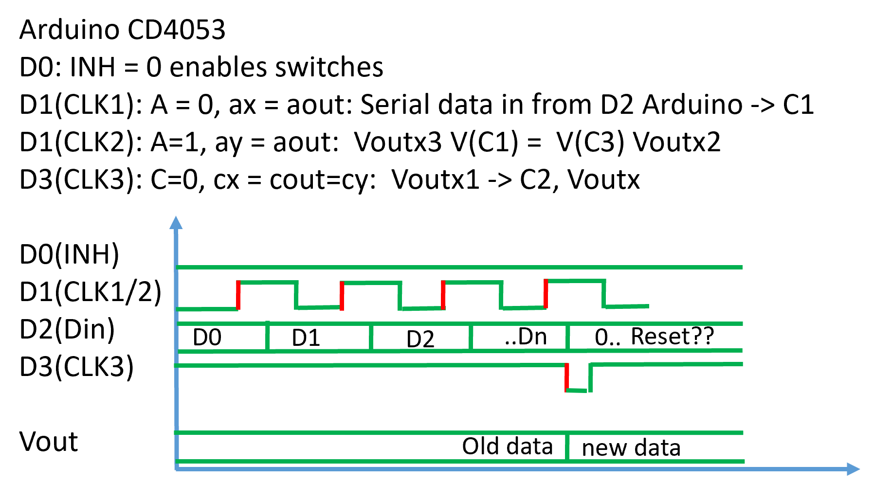
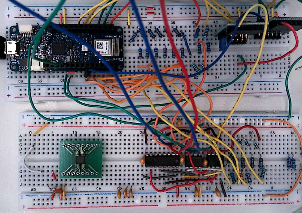
C serial Breadboard Circuit
|
CD4053 3 2:1 MUX circuit MCP6022 rail-to-rail Opamp C1,C2,C3 capacitors Wiring list in handout POMOD DA2, AD2 |
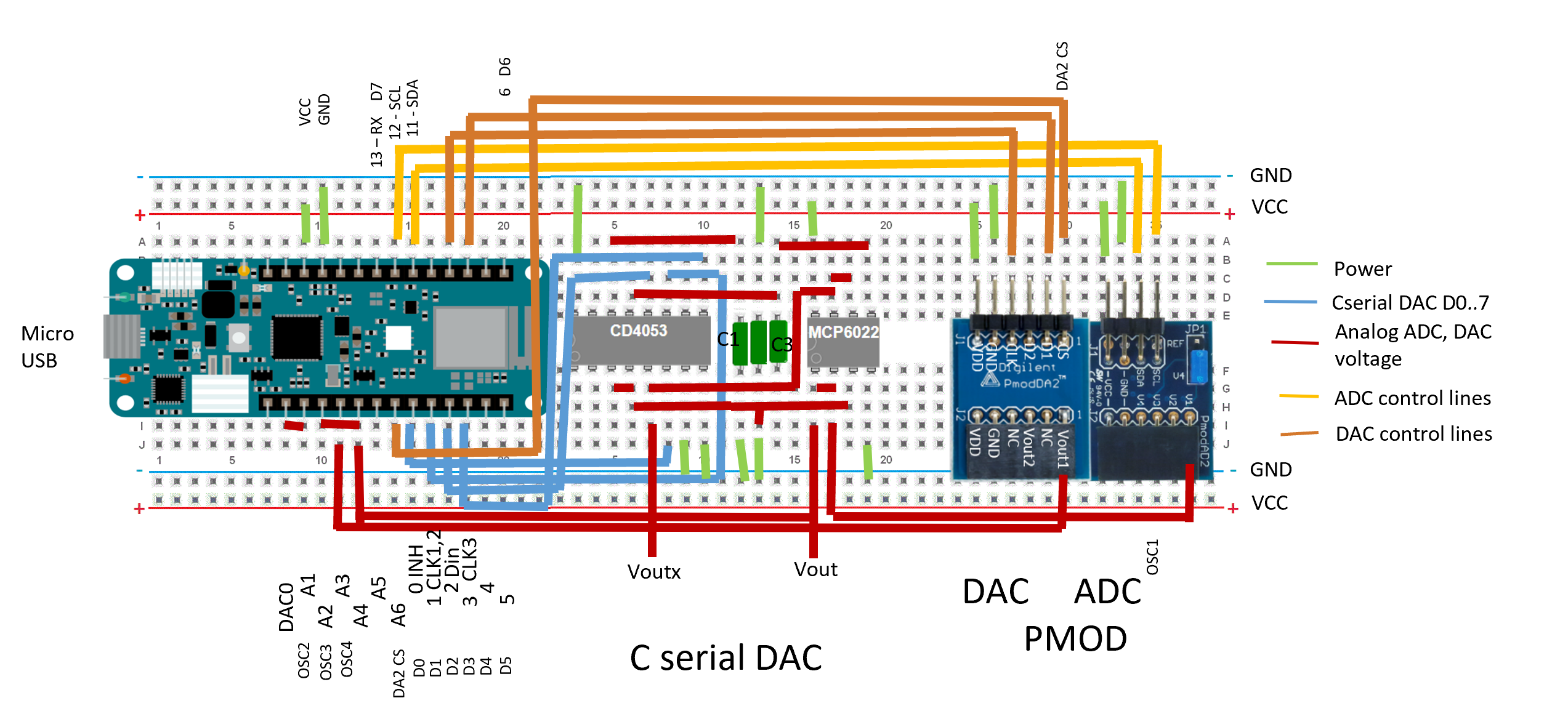 |
Wiring list: 19 wires
CD4053 Pin 16 VDD - 3.3V
CD4053 Pin 7 Pin 8 – GND
CD4053 Pin 6 INH – D0 Arduino
CD4053 Pin 11 A CLK1,CLK2 – D1 (OSC1)
CD4053 Pin 12 AX – D serial data in D2 Arduino (OSC2)
CD4053 Pin 13 AY – C3, MCP6022 pin 5 INB+
CD4053 Pin 14 AC – C1
MCP6022 Pin 8 VDD – 3.3V
MCP6022 Pin 4 VSS – GND
MCP6022 Pin 6, Pin7 – CD4053 Pin5 Cx (OSC3)
CD4053 Pin3 Pin4 Cy, Cc – C2, MCP6022 Pin 3
CD4053 Pin 9 C CLK3 – D3 Arduino sample and hold control
MCP6022 Pin1, Pin2 – C serial analog voltage out A2 Arduino (OSC4)
CD4053: RDSon = 470 Ohm at VDD = 5V.
CD4053: Cos = 9 pF, CL = 50 pF.
CD4053: fbw = 20 MHz, crosstalk 65mV peak VDD = 15 V
C1, C3 (223)= 22nF; C2(333) = 33nF
tsettlingLH = 400us, tsettlingHL = 600us, 3V
DataConverterCharV5 activeS = 20 is 100us.
Arduino Software C serial
Software ArduinoC serial DAC StartServerAx.bat Arduino/DataConverterCharV5/DataConverterCharV5.ino Specific: Pin definitions Timing sequence |
 |
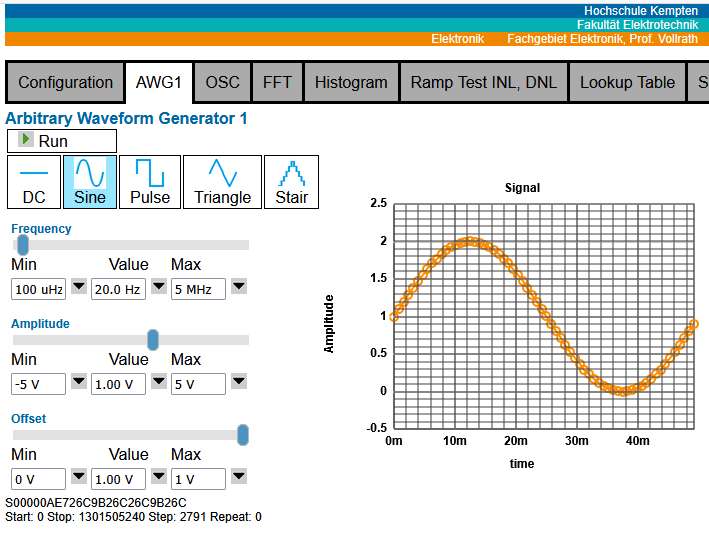
Waveform selection: frequency, offset, amplitude
Data acquisition oscilloscope: timing, number of samples
Lookup table
User interface (.html), server software (.bat, .js) and Arduino software (.ino) have to match to work.
R2R DAC
Arduino/DataConverterChar
DataConverterCharV5.ino
...

/* C serial  CD4053  and MCP6022 */
#define DAC_INH          0
#define DAC_C12          1
#define DAC_Dx           2
#define DAC_C3           3

...

/* Init  C serial control lines */
  pinMode(DAC_INH, OUTPUT);
  pinMode(DAC_C12, OUTPUT);
  pinMode(DAC_Dx, OUTPUT);
  pinMode(DAC_C3, OUTPUT);

 digitalWrite(DAC_INH, LOW); // INH low activates switches
 digitalWrite(DAC_C12, LOW); // CLK12 coonnects Dx with C3
 digitalWrite(DAC_Dx, LOW); // Data line low
 digitalWrite(DAC_C3, HIGH); // output disconnected from Voutx1

...

int activeS = 20; // 1 tested Time switches are closed for charge redistribution 1 makes 30/2048 error at 10 pF
int nBits = 9;    // number of send bits

/* C serial digital write */
void digWrite(uint16_t sineValue){
  digitalWrite(DAC_C12, LOW);
  digitalWrite(DAC_C3, HIGH);
  digitalWrite(DAC_Dx, LOW);
  delayMicroseconds(activeS*5);
  // write zero
  for (int i3 = 0; i3 < nBits; i3++) {
        digitalWrite(DAC_C12, HIGH);
        delayMicroseconds(activeS*5);
        digitalWrite(DAC_C12, LOW);
        delayMicroseconds(activeS*5);
  }
    // shift nBits bits in  18ms??
  for (int i3 = 0; i3 < nBits; i3++) {
     if ((sineValue & bitsX[i3]) == bitsX[i3] ) {
        digitalWrite(DAC_Dx, HIGH);
     } else {
        digitalWrite(DAC_Dx, LOW);
     }
     digitalWrite(DAC_C12, HIGH);
     delayMicroseconds(activeS*5);
     digitalWrite(DAC_C12, LOW);
     delayMicroseconds(activeS*5);
  }
  // transfer to output
  digitalWrite(DAC_C3, LOW);
  delayMicroseconds(activeS*5);
  digitalWrite(DAC_C3, HIGH);
}
...
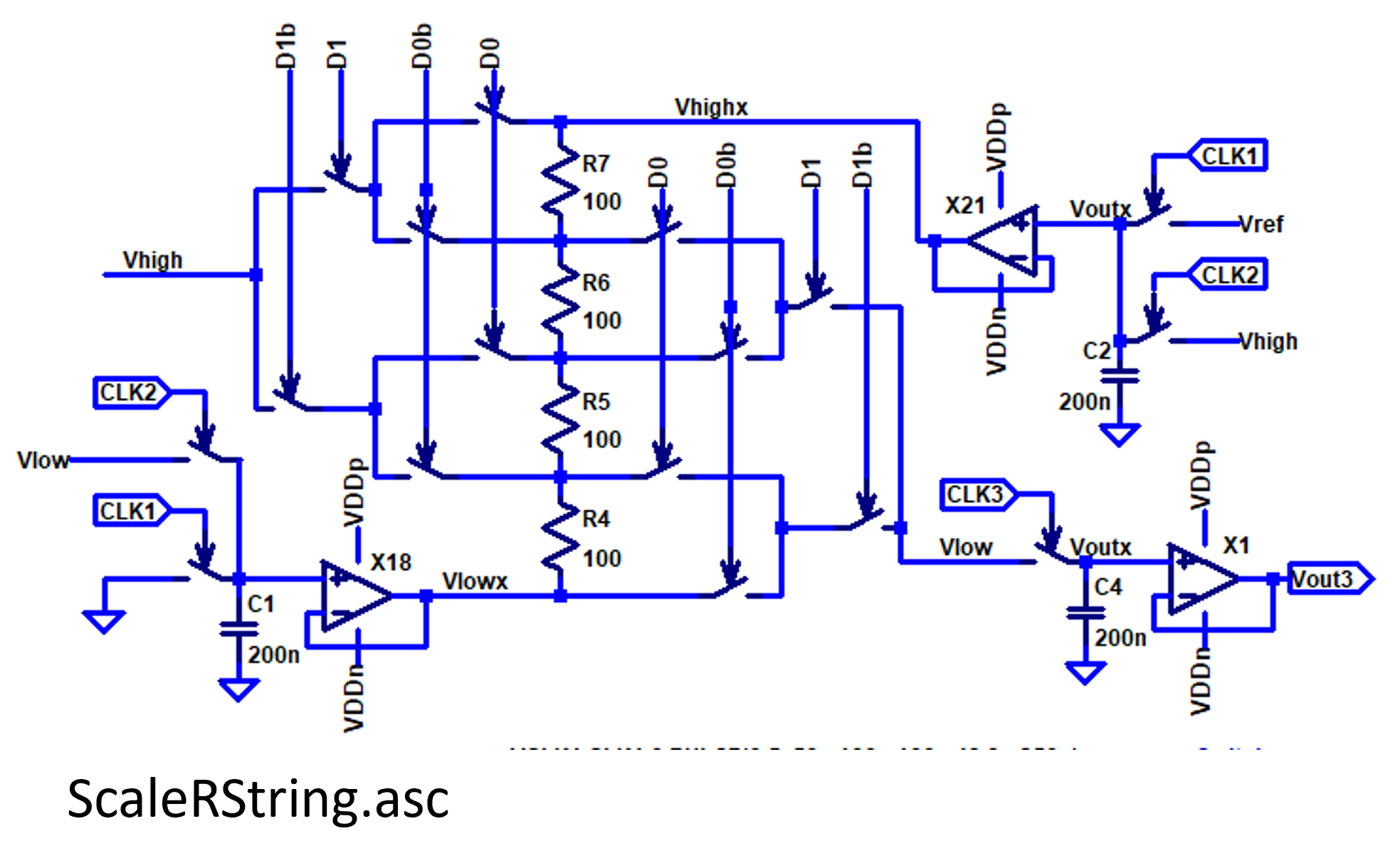
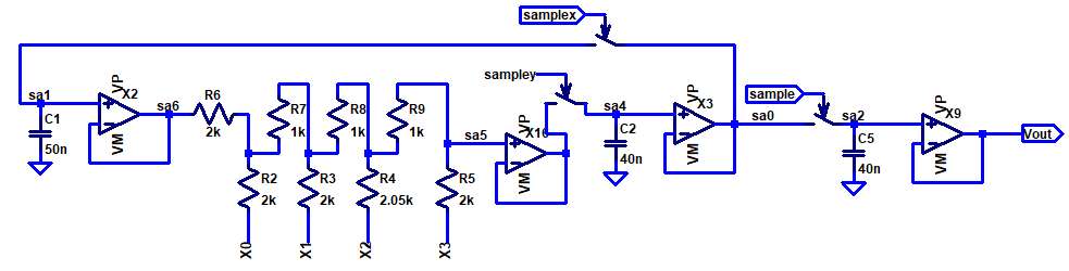
Data Converter Circuits
 |
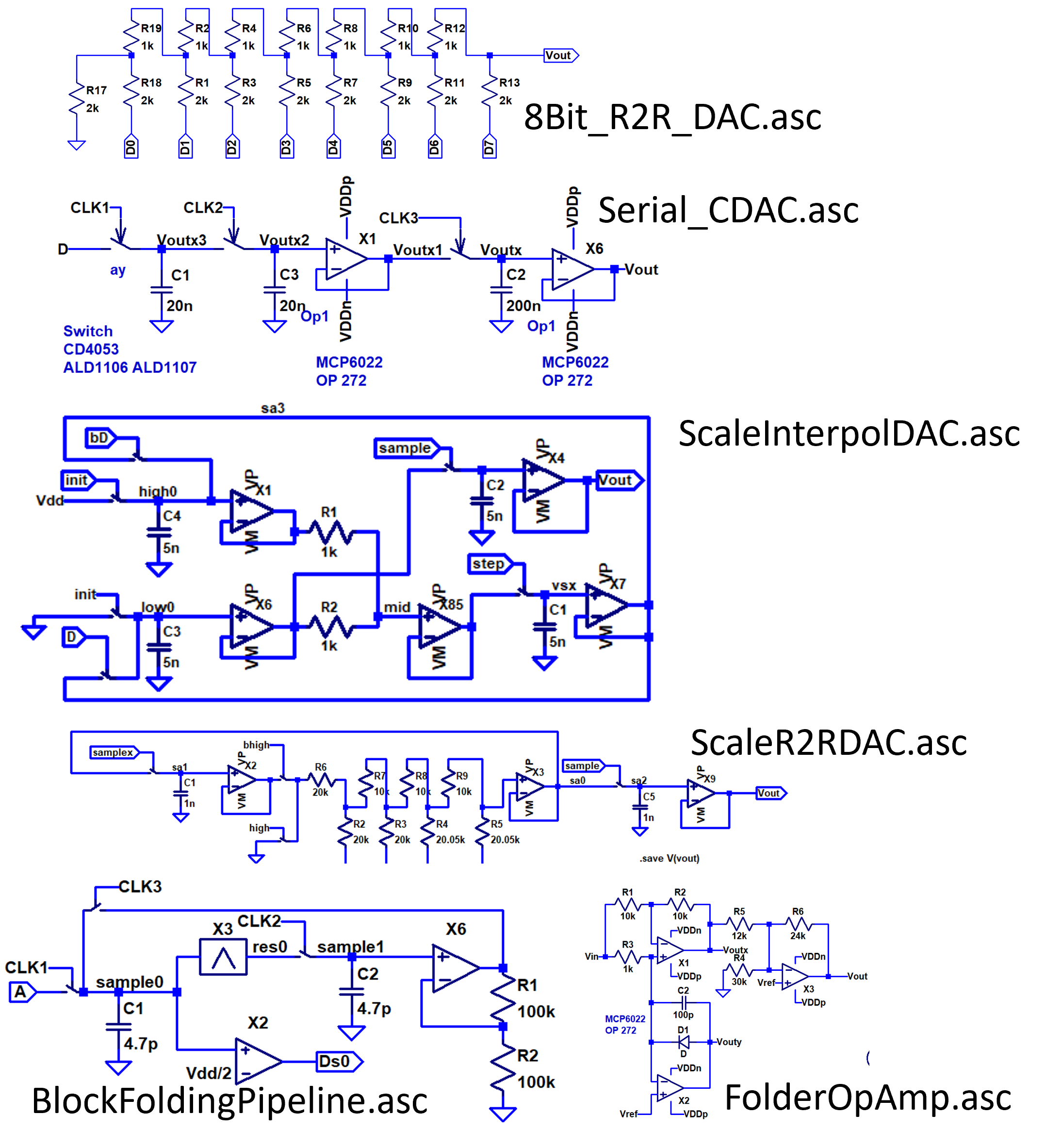 |
- 8-Bit R2R DAC: 8Bit_R2R_DAC.asc
- Scalable C serial DAC: Serial_CDAC.asc
- Scalable R2R DAC: ScaleR2RDAC.asc
- Scalable interpolating DAC: ScaleInterpolDAC.asc
- Scalable interpolating DAC SAR ADC: BlockCserialSARADC_01.asc
- Scalable folding pipeline ADC:
BlockFoldingPipeline.asc,
FolderOpAmp.asc
- 8 Bit mixed DAC: 8Bit_RLR2RMix_DAC2.asc
- Sigma Delta ADC (FPGA)
Cyclic R2R DAC Schematic
|
The schematic shows a cyclic R2R DAC. |
 The resolution NBit can be controlled via software. |
It is easy to scale this architecture via software.
Tradeoff between timing and resolution.
Arduino Schematic
0 D0
1 D1
2 D2
3 D3
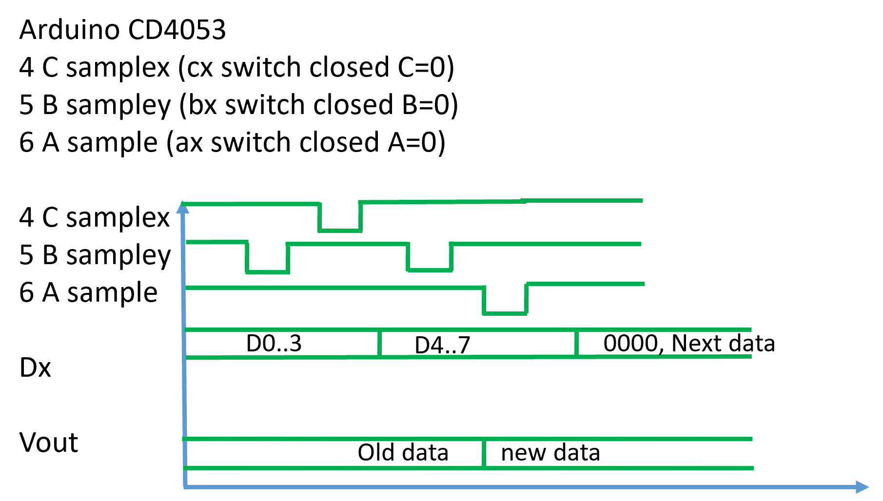
4 C samplex (cx switch closed C=0)
5 B sampley (bx switch closed B=0)
6 A sample (ax switch closed A=0)
Pin 6 CD4053 Inhibit 0 V
Pin 7 CD4053 VEE 0 V
Pin 8 CD4053 VSS 0 V
Pin 16 CD4053 VDD 5 V
Pin 4 MCP6022 GND 0 V
Pin 7 MCP6022 VDD 5 V
90 min from schematic to Breadboard.
At the start once a D = 0000 can be set for intialization.
This is not mandatory.
Compare 8-bit R2R DAC signal with signal after MCP6022 Opamp buffer, after closed switch with MCP6022, and with active sample switch with MCP6022.
What happens at activating only sampling output at the end? Implemented
What happens at different sampling/off times (activeS, offS)?
What happens at lower sampling capacitances (Cx)?
What happens with different R2R resistances (Rx)?
What happens with INL, DNL range of 255 (, 512, 1024, 4096)?
Does OP1A need some gain?
Implement/Use lookup table for 256, 12-bit values
sine8 = lookup8[sine8]; -> sine12x = lookup8[sine8];
Identify capacitances with RC-low pass bode plot using 1MOhm resistance/open.
What about using Ts3a44159 as MUX at 3.3 V?
Tradeoff between timing and resolution.
Arduino Schematic
0 D0
1 D1
2 D2
3 D3
4 C samplex (cx switch closed C=0)
5 B sampley (bx switch closed B=0)
6 A sample (ax switch closed A=0)
Pin 6 CD4053 Inhibit 0 V
Pin 7 CD4053 VEE 0 V
Pin 8 CD4053 VSS 0 V
Pin 16 CD4053 VDD 5 V
Pin 4 MCP6022 GND 0 V
Pin 7 MCP6022 VDD 5 V
90 min from schematic to Breadboard.
At the start once a D = 0000 can be set for intialization.
This is not mandatory.
Compare 8-bit R2R DAC signal with signal after MCP6022 Opamp buffer, after closed switch with MCP6022, and with active sample switch with MCP6022.
What happens at activating only sampling output at the end? Implemented
What happens at different sampling/off times (activeS, offS)?
What happens at lower sampling capacitances (Cx)?
What happens with different R2R resistances (Rx)?
What happens with INL, DNL range of 255 (, 512, 1024, 4096)?
Does OP1A need some gain?
Implement/Use lookup table for 256, 12-bit values
sine8 = lookup8[sine8]; -> sine12x = lookup8[sine8];
Identify capacitances with RC-low pass bode plot using 1MOhm resistance/open.
What about using Ts3a44159 as MUX at 3.3 V?