Hochschule Kempten      
Fakultät Elektrotechnik      
Interface Electronics       Fachgebiet Elektronik, Prof. Vollrath      

Interface Electronics

Laboratory 01

GroupA1,****06, A


Overview

Webpage Installation

Test for 4 Bit ADC and DAC

- A 4 Bit ADC and DAC test is simulated in LTSPICE
- The files are donloaded and LTSPICE are started.

- The output file size can be limited by using .save dialog option.

- Voltage source was added with a ramp from 0-1V with rise time of 655 µs.

- The picture shows a ramp in the voltage and DAC ramp output voltage over
16 steps are observed.

- Using the following .meas (measurement) statement to find the voltage levels.

- 0.0625V is given for the code 000 at time 60 µs.
No error in the voltage level is seen. It is an ideal ADC and DAC.


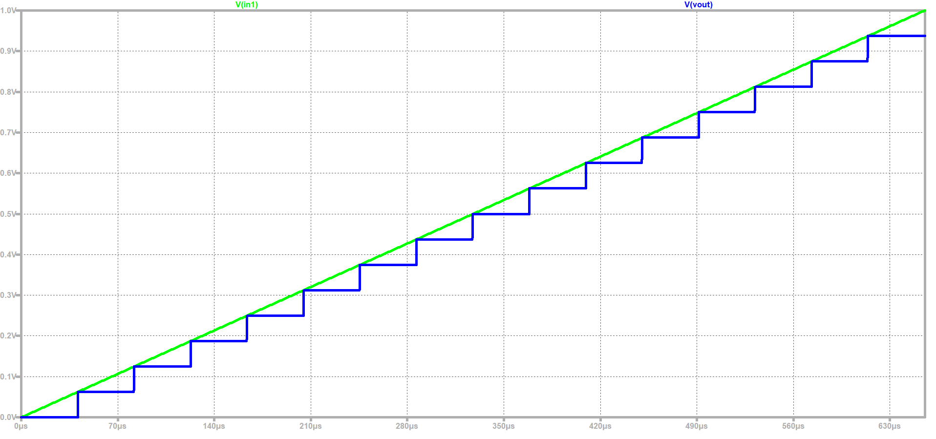
LTSPICE Schematics of 3Bit DAC


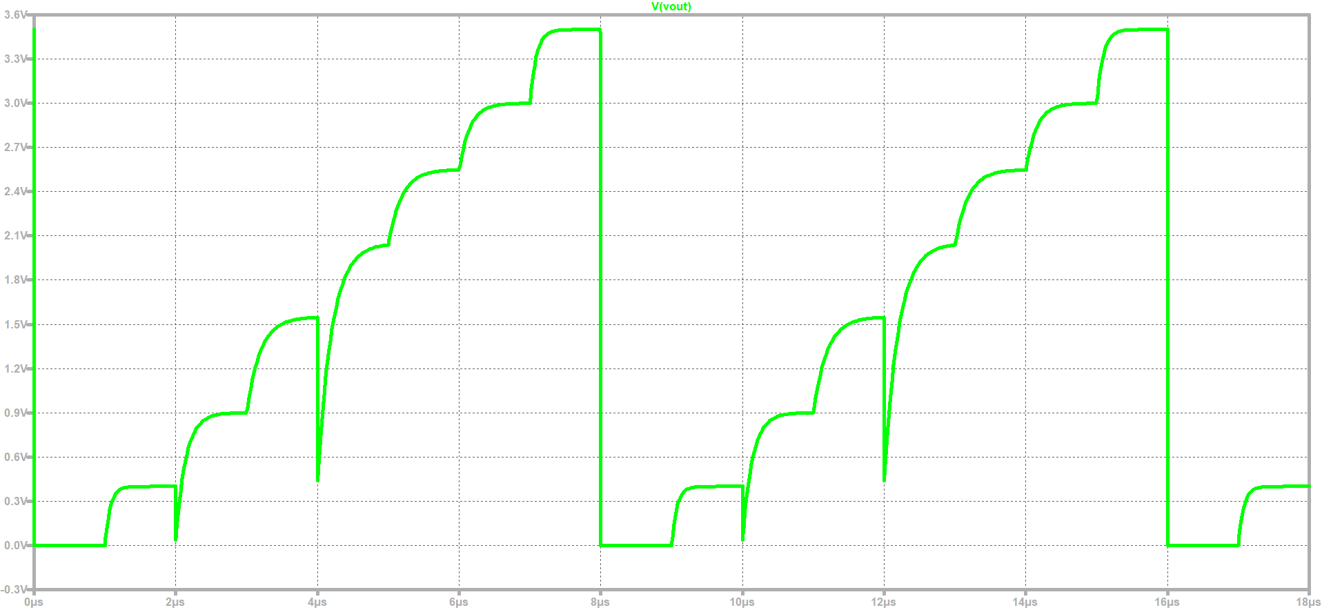
Using the following .meas statement, the voltage levels are measured

.meas tran V0000 FIND V(Vout) AT=0.9µs

Similarly, At 1.95µs the voltage is shown as follows;

V0001: V(Vout)=0.399999V at 1.95e-006

The given 3bitDAC circuit is totaly operated on transitor based switching.

The spikes in the ouptup are becasue of the switching of the transistors .

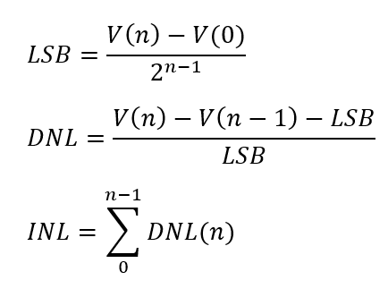
DNL and INL Analysis

  • The DNL and INL values are calculated by using the following formulas

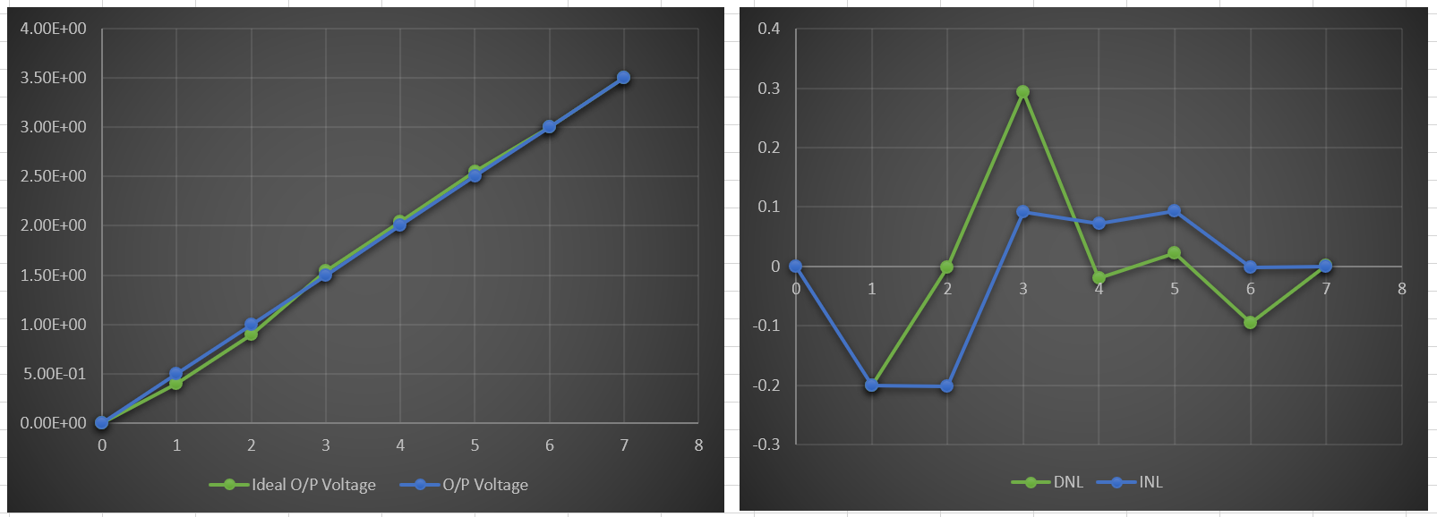
  • The graphs for the DNL, INL and Output voltage and Ideal Output voltage are shown below;

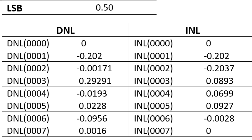
  • and their values are summarized in the following Table

Summary

  • A 4bit DAC and ADC is simulated in LT Spice and its output is analyzed
  • No errors are observed in the ramp output voltage
  • ALso a 3bit DAC is simulated on LTSpice and its output is analyzed
  • Finally the complete lab tasks are reported in a webpage
  • Note++ and Adobe Dreamviewer have been used to develop the webpage

References


[1] Making of a Webreport , Vollrath