Hochschule Kempten      
Fakultät Elektrotechnik      
Interface Electronics       Fachgebiet Elektronik, Prof. Vollrath      

Interface Electronics

Laboratory 03: ADC DAC Analysis

GroupA1,****06, A


Overview

Schematic for ADC & DAC

  • The circuit is downloaded from the internet: Vollrath InEl>LTSPICE>Scalable behavioral 4 But DAC>download files"4Bit_pipe.asc, sample_hold.asc, sample_hold.asy".
  • The 4 Bit ADC is downloaded from the next circuit on the webpage. Downloaded files: "4Bit_ADC_pipe.asc, Switch.asc, Switch.asy".
  • At last the final circuit is downloaded form the same wwebpage: Fiel name "4Bit_ADC_DAC_pipe.asc".
  • The final circuit is opened in LTSPICE for futher simulation and analysis as explained below.

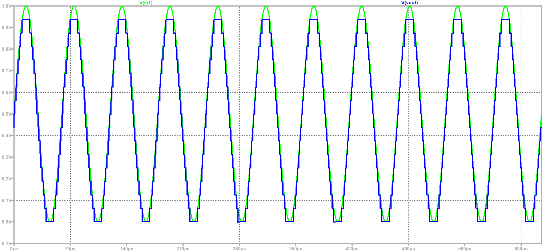
  • 4 Bit ADC and DAC simulation for Sine Wave

    - A 4 bit ADC DAC with ideal components is simulated with sine wave as input signal.

    - THe input analogue signal (green wave) and output digital to analogue coverted signal (blue wave) is shown in the adjacent graph..


    - The ideal plot can be later compared with the real output of the implemented circuit.


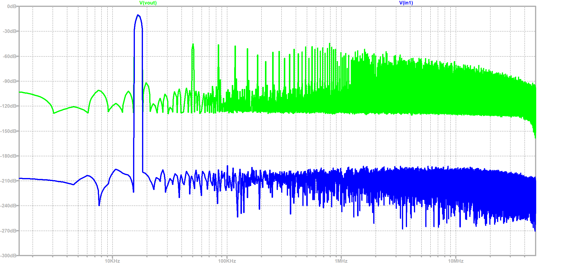
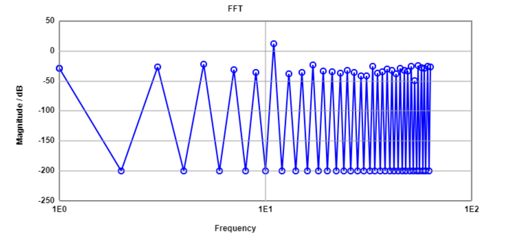
    FFT of 4 Bit ADC and DAC with Sine input

    - A FFT of 4 Bit ADC abd DAC is done by LTSPICE.

    - The number of data points samples are set as 65536..


    - The signal to noise of both the input and output signals and it is observed that input signal has better input to nosise level because we have only 4 bit.


    - Since LTSPICE doesn't provide all the values so we need external data processors.


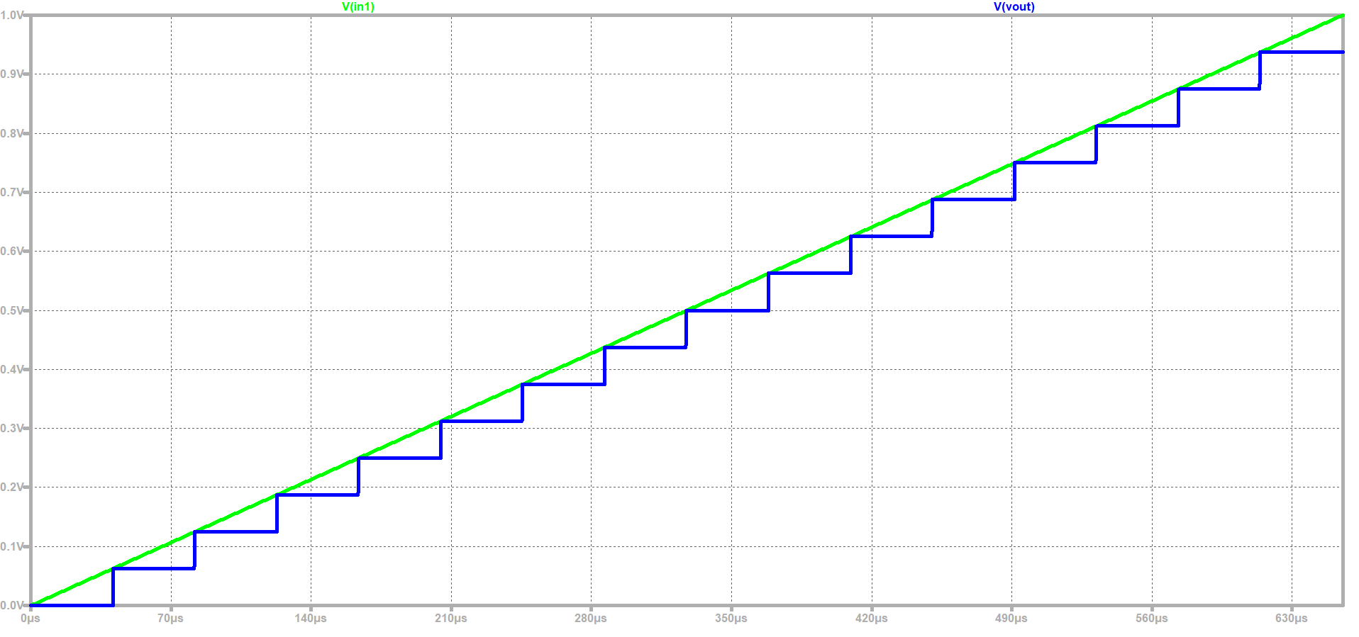
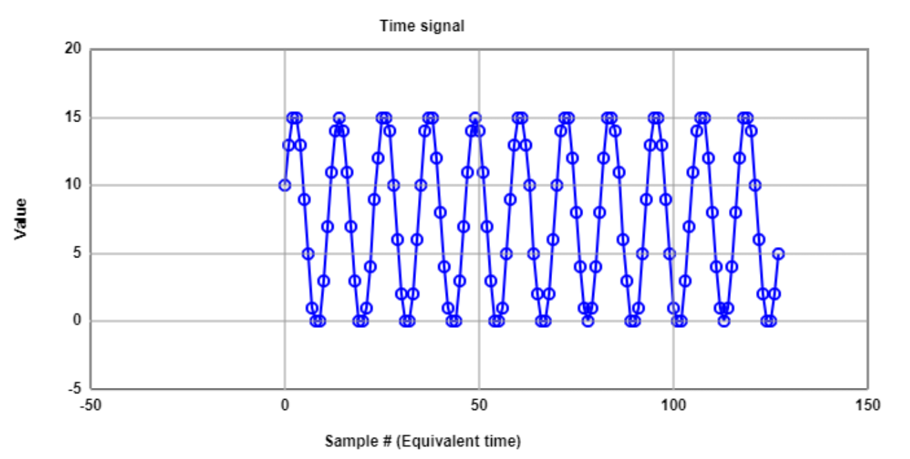
    Ramp Test of DAC ADC

    - Ramp test is performed for FFT to check signal to noise.

    - Another voltage source is required for ramp and that is added by the following command.
    - V1 in1 0 PULSE(0 1 0 655.36u 655.36u 0 1310.72u)


    - Since LTSPICE simulation has varied step size so so to extract data poitns we need external data processors.

    \


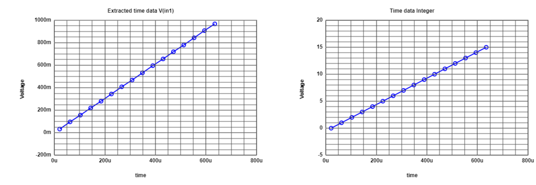
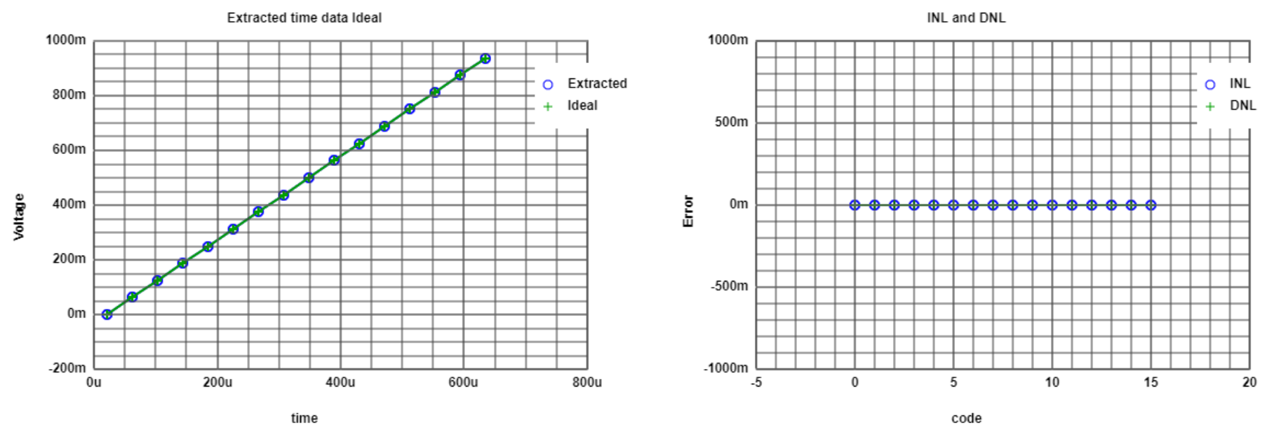
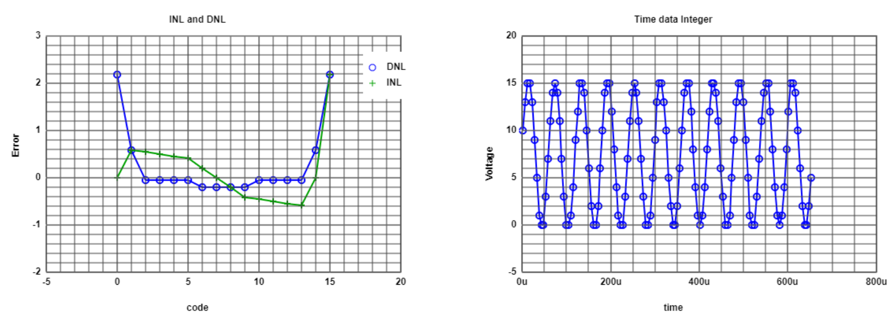
    Data Analysis for Ramp Signal


    - Since the transfer curve generated by LTSPICE has lot of points and we require filter.

    - For filteration I have used an online Javascript tool that can be accessed at InEl-Lab 3 webpage > ADC DAC Analysis > Read Raw File.

    - The start time (0), stop time (655.36u) and the time step (40.96u) is used for the simulation.

    - The javascript tool gives the graph the extracted values in real numbers .

    - The extracted values are mapped to integer (shown in the adjacent image) in the range of 0-15, the integer values are generated in the table that can be further used for the FFT analysis (another javascript tool).

    - The

    - Finally the DNL and INL is performed by the using the same javascript tool as shown in the graph below.

    - For further histogram test, to increase the time steps the step time is changed to 5.12u.

    - The DAC INL, DNL graph is shown is also pasted below. The blue stepped curve corresponds to the extracted values while the green dotted curve shows ideal one.


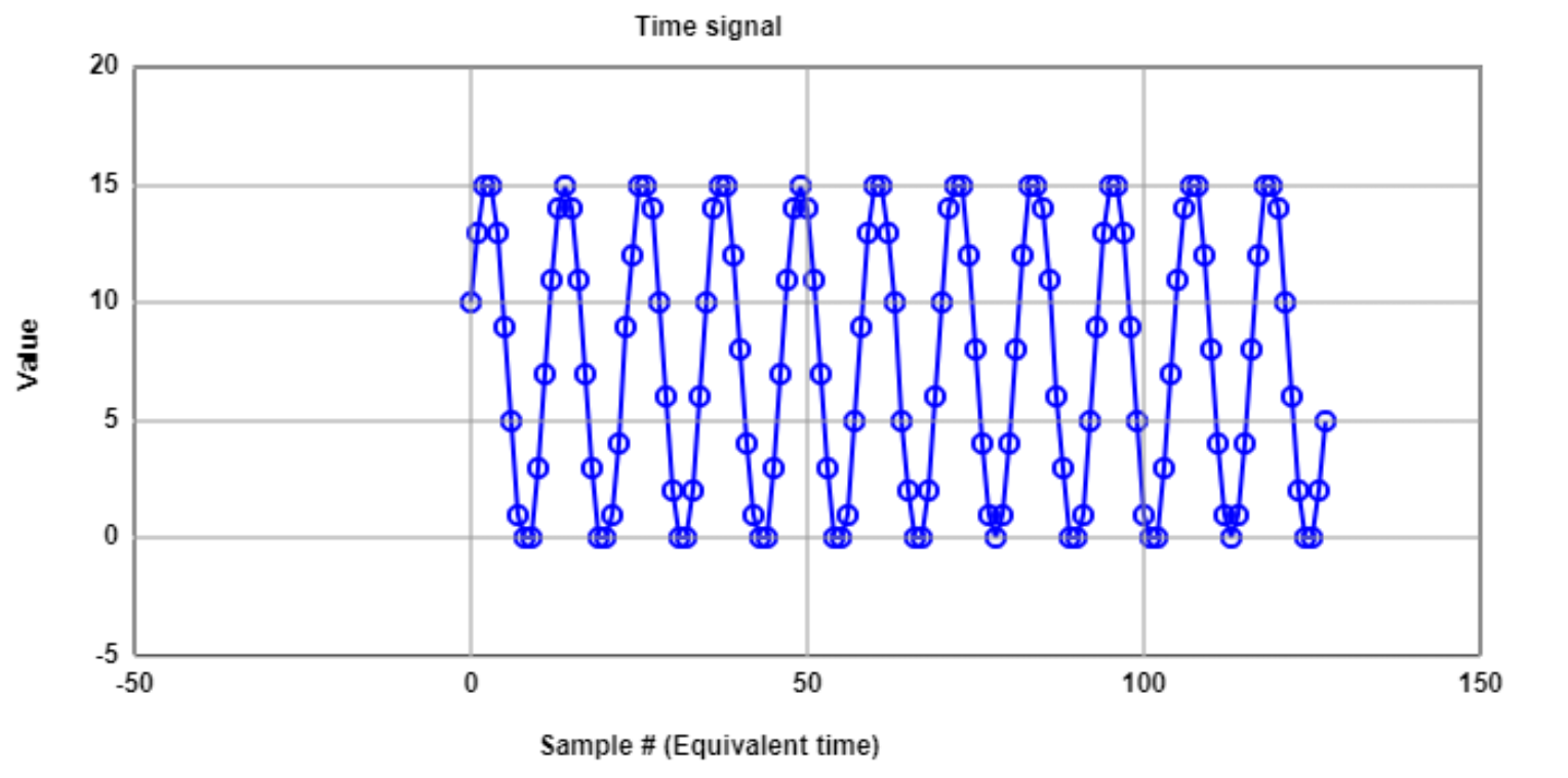
    Data Analysis for Sine Input


    - Now the since input is activated and the ramp is deactivated in the LTSPICE.

    - The updated LTSPICE is again uploaded to InEl online javascript tool.

    - Again the extracted values are mapped to integer in the range of 1-15.

    - The ADC histogram test is shown in the adjacent graph. A typical curve of the since funciton is sobserved and the DNL and INL are calulated by an average value. Although the value is not real but is compared to an average value.

    - Furhter it is mapped to integer to extract the values for the FFT.

    - The values are copied for further FFT analysis. The link to javascript tool is accessed by the provided FFT analysis link belwo the integer values at the end of the webpage.

    - The copied integer values are pasted into the "Input data" section of the "ADC FFT Javascript Spectrum Analysis Tool".

    - After using the "Read positive integer data" the general charts are generated (web button on online tool).

    - The generated FFT graph has missing values when simulated for 10 bits. Therefore, the FFT and INL/DNL graphs are again generated at 4 bits, and the FFT and INLDNL graphs are also pasted below.


    R2R DAC Simulation

    - The adjacent schematic shows the 4-Bit R2R DAC

    - The schematic is used for the ADC DAC simulation for error analysis.


    - To introduce some error the values of the resistors are modified to 1.5k and 1.3k ohm.


    - Finally a sine test is simulated and INL, DNL are calulated usign InEl javascript tool.

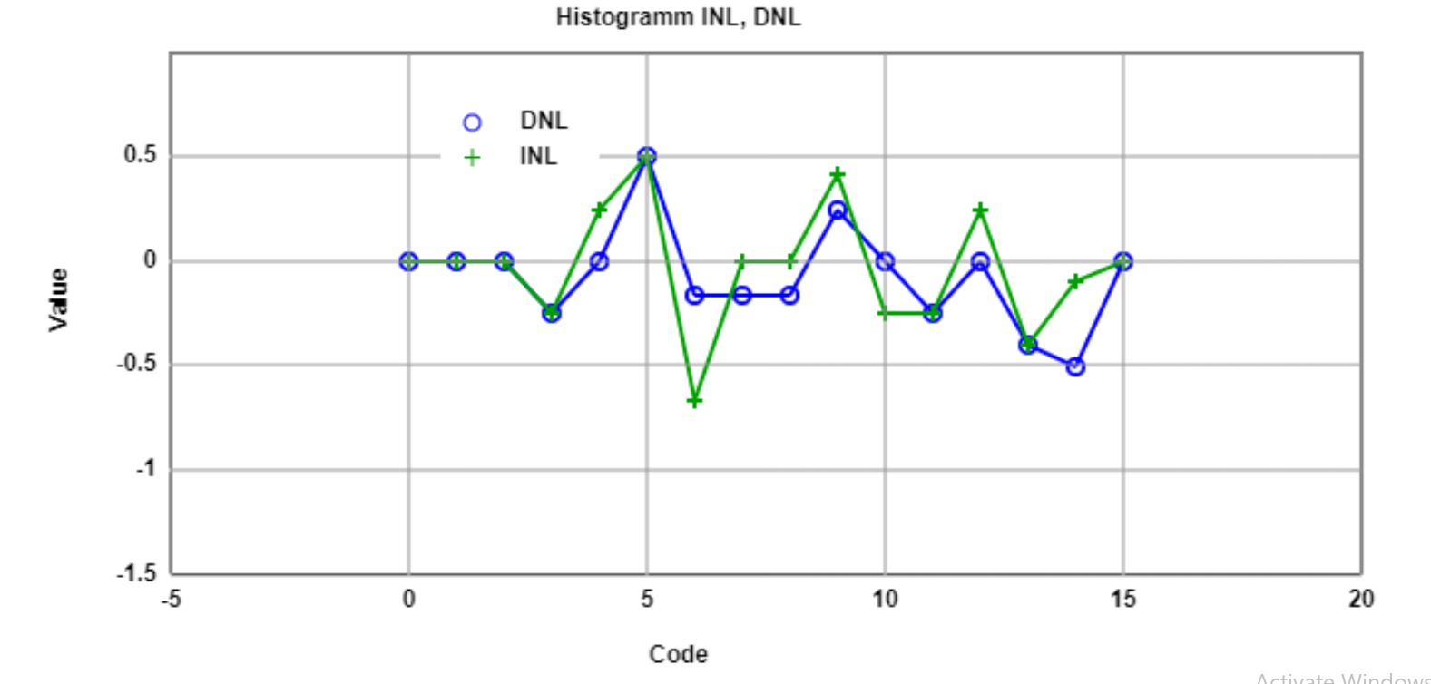
    - The Histogram and INL and DNL values are shown in the following graphs.


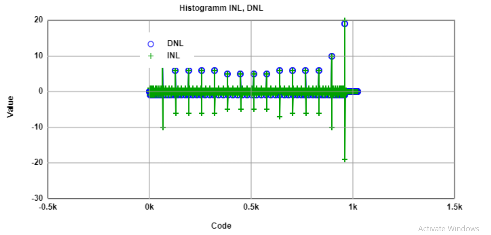
    - Now a ramp test is simulated and INL, DNL are calulated and the Histogram with INL and DNL values are shown in the following graphs.


    Summary

      In this laboratory assignment, I have performed analysis of an ideal ADC and DAC circuit. I have introduced the error via changing the values of resistor to observe the error in the ADC DAC circuit. The sine and ramp analysis are conducted and FFT spectrum, SNR, INL, DNL Histogram are observed. While reporting my findings, I have also learned how to make 2x2 table to better format the graphs and text in an HTML webpage.

    References


    [1] Making of a Webreport , Vollrath