The set up of 4 bit ADC and DAC
If the given set up is analyzed, it consists of 2 parts. First is the Analog to Digital Converter which has analog voltage input
and 4 digital outputs (e.g. D0 and D1). Each output is coded binary (0 and 1). Here the analog signal is sampled and coded with
binary coded at the 16 voltage levels and then transfered to the second part of the set up, Digital to Analog Converter. At this
part, the coded information is converted into back to Analog input signal.
- For the ramp and sine simulation different LTSPICE directives are written.
LTSpice Simulation Results of 4 bit ADC and DAC With Ramp and Sine Input Signal
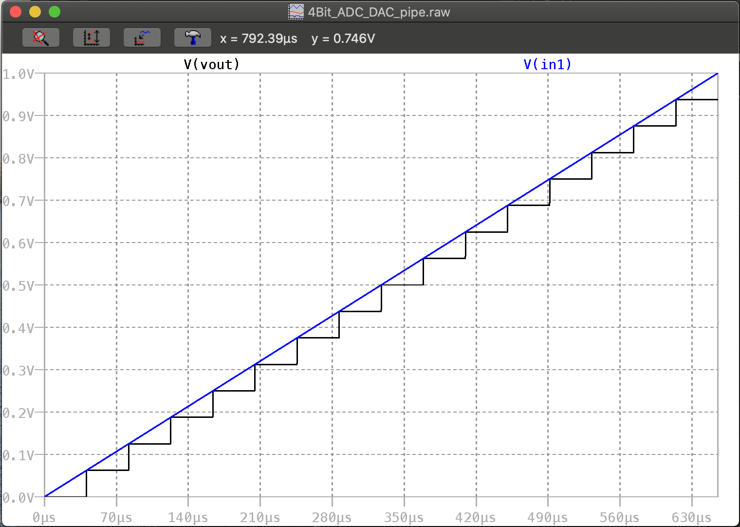
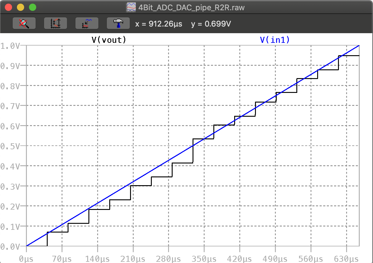
The figure shows a input signal of ramp starting from 0 V to 1V and output signal with steps. The input signal is the blue line
and the digital put signal is shown by black color. Due to it's bits number of 4, 2^4=16 steps are present in the figure.
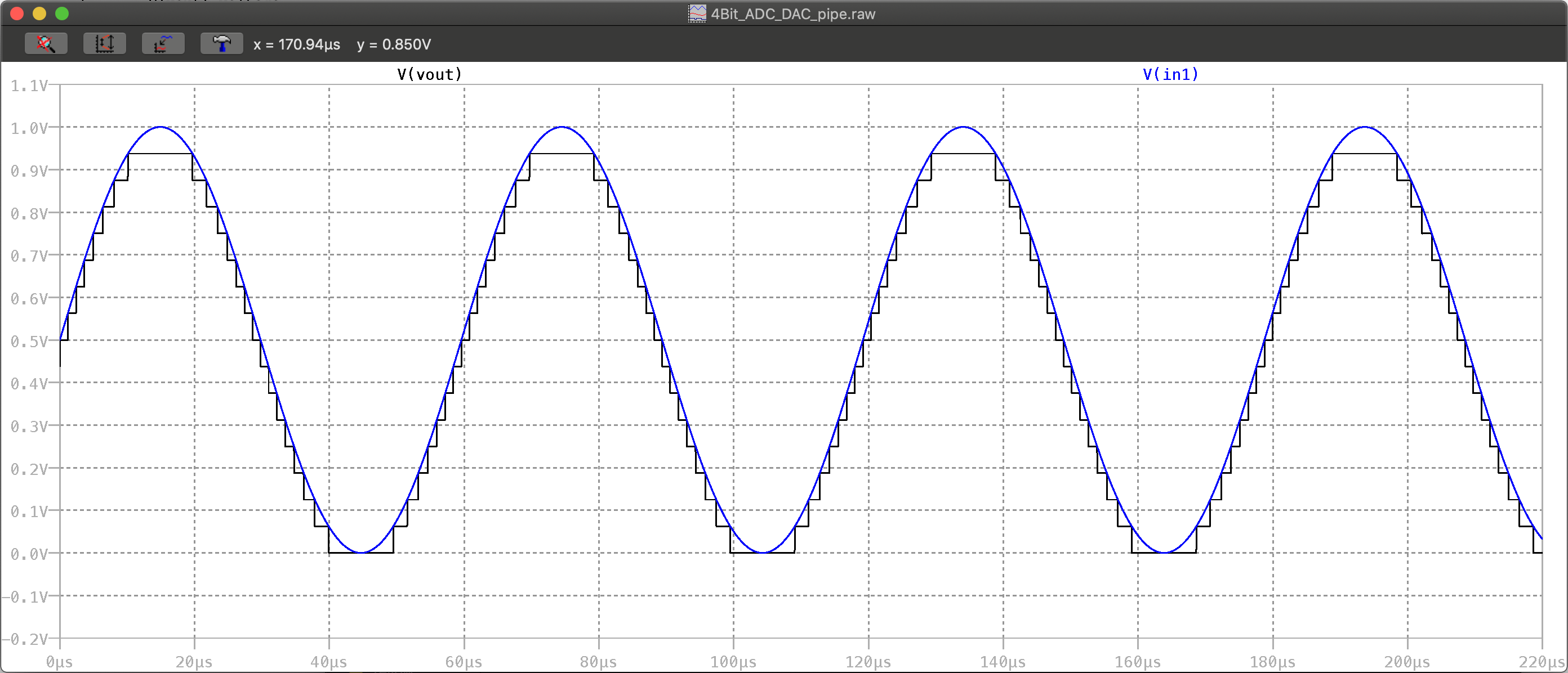
The figure below shows the the sine input and output signals oscillating between peak to peak voltage of 1 V.
Blue indicates the analog sine input signal and the black digitalized and converted back to analog signal
Moreover, the step size of 16 can also be seen.
- Both figures are obtained directly from the LTSpice simulation by using different directives.
Simulation Results of 4 bit ADC and DAC with Ramp Input Signal by Simulator of Read Raw File
|
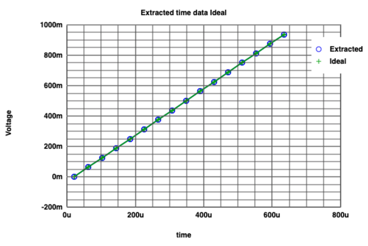
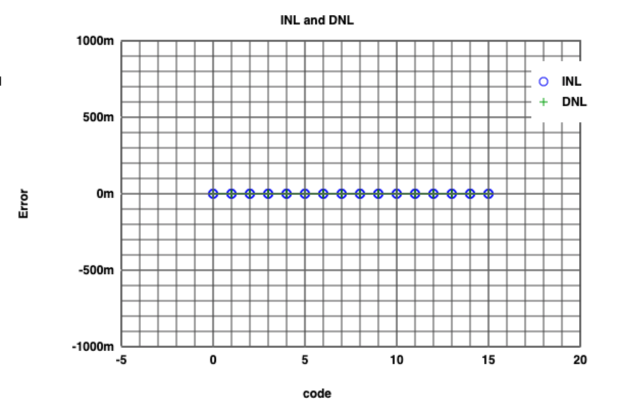
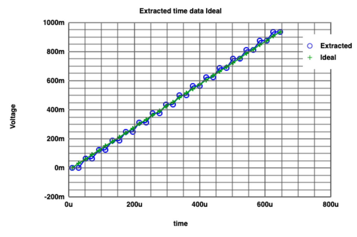
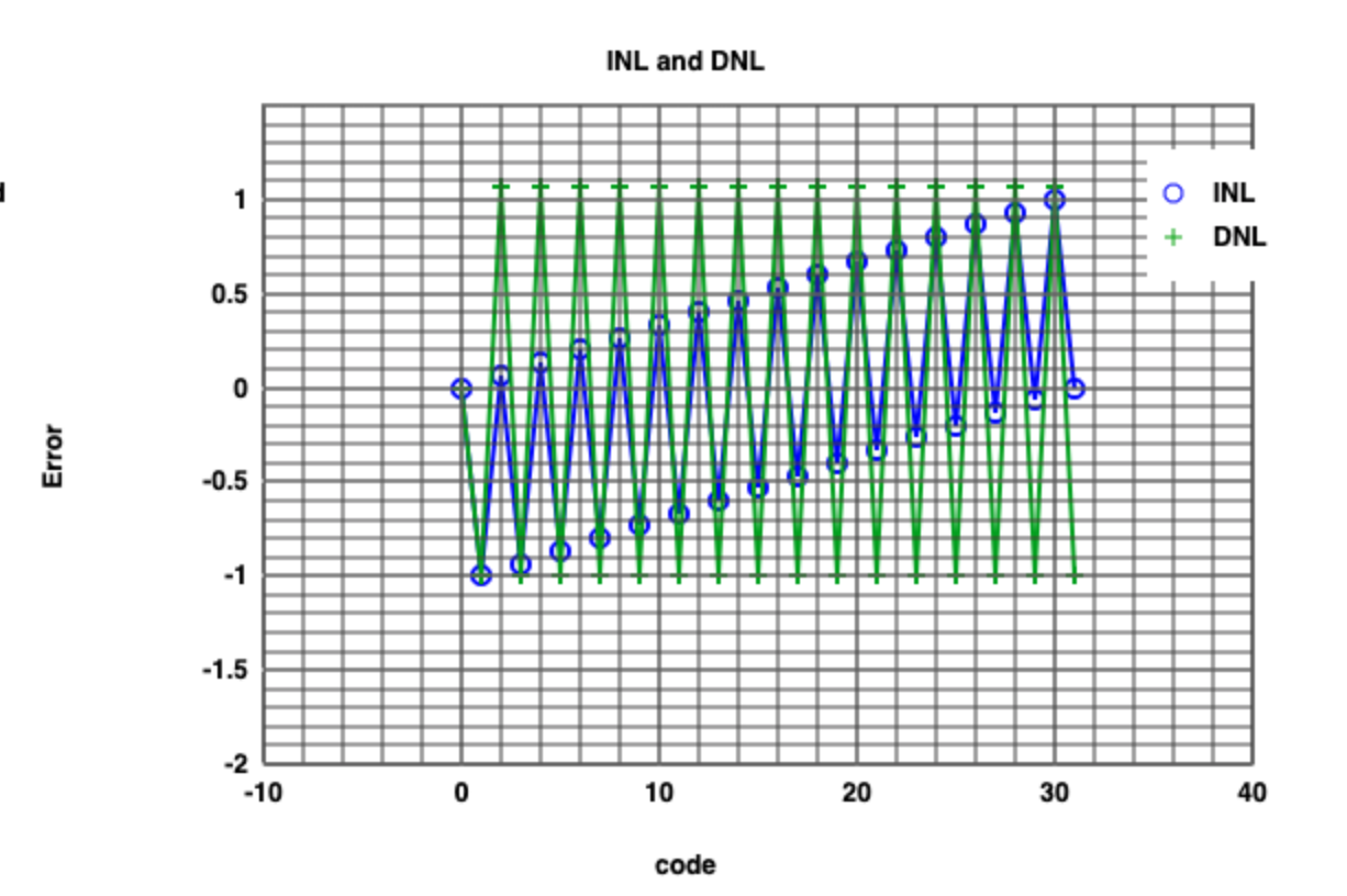
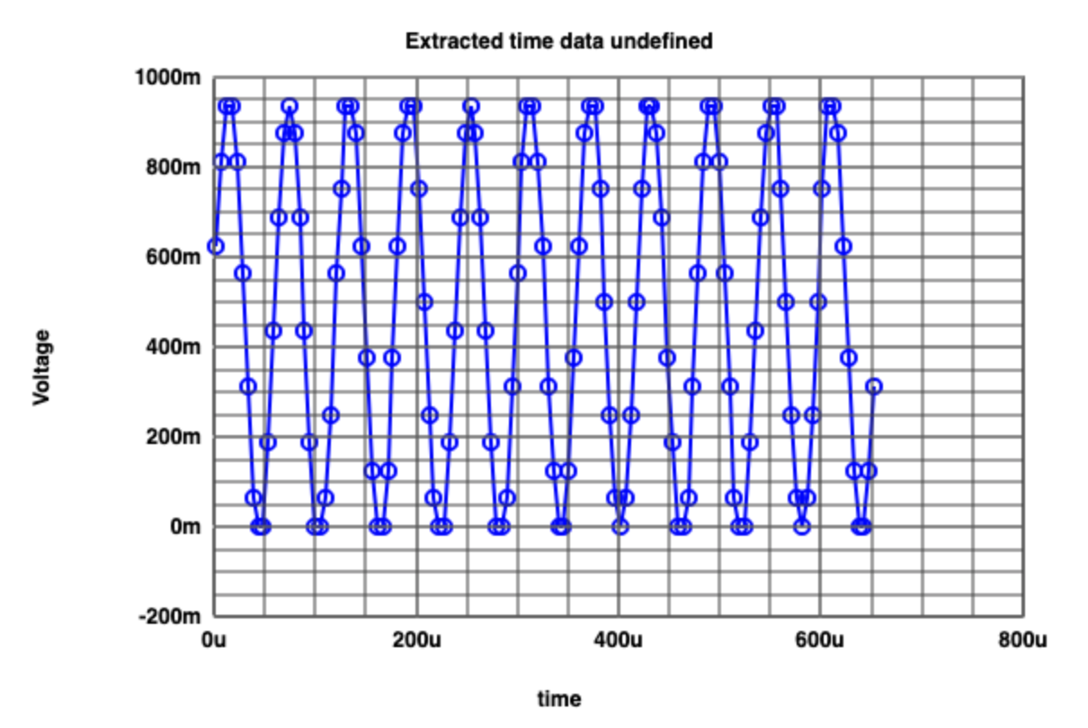
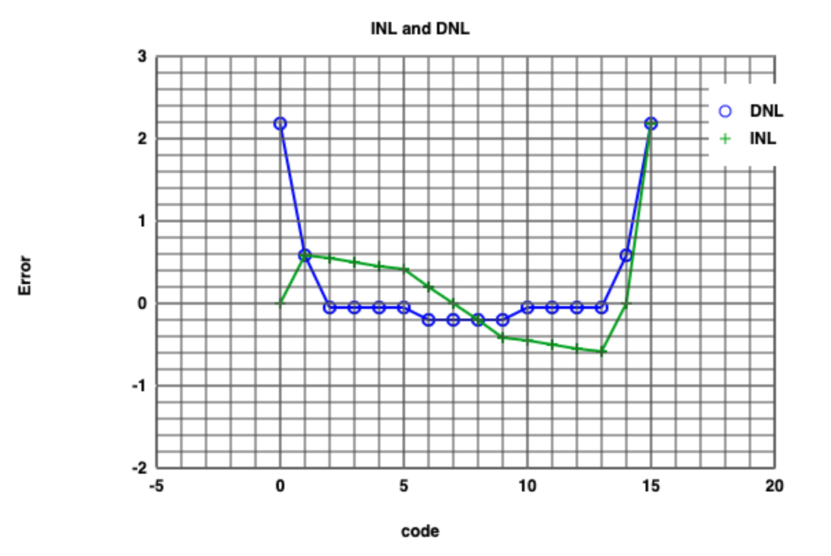
On the upper right side, the simulation result of Read Raw File from 4 bit ADC and DAC. The sampling rate is chosen as 40.96 µs which means it is sampled every 40.96 µs.The blue color is the extracted values at the sample points and the green color for the ideal values. When these two are compared, now difference is visible On the lower right side, the errors of DNL and INL can be seen for every step which is assumed none.
|
  |
Simulation Results of 4 bit ADC and DAC with Ramp Input Signal by Simulator of Read Raw File
|
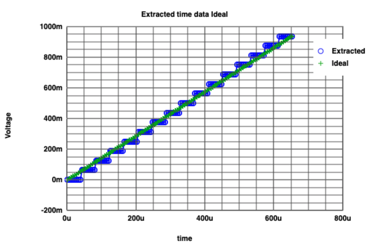
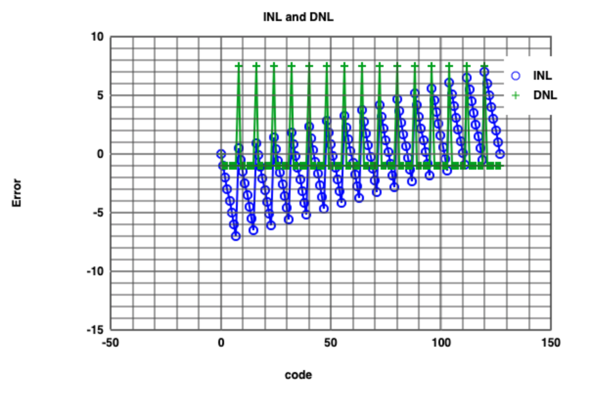
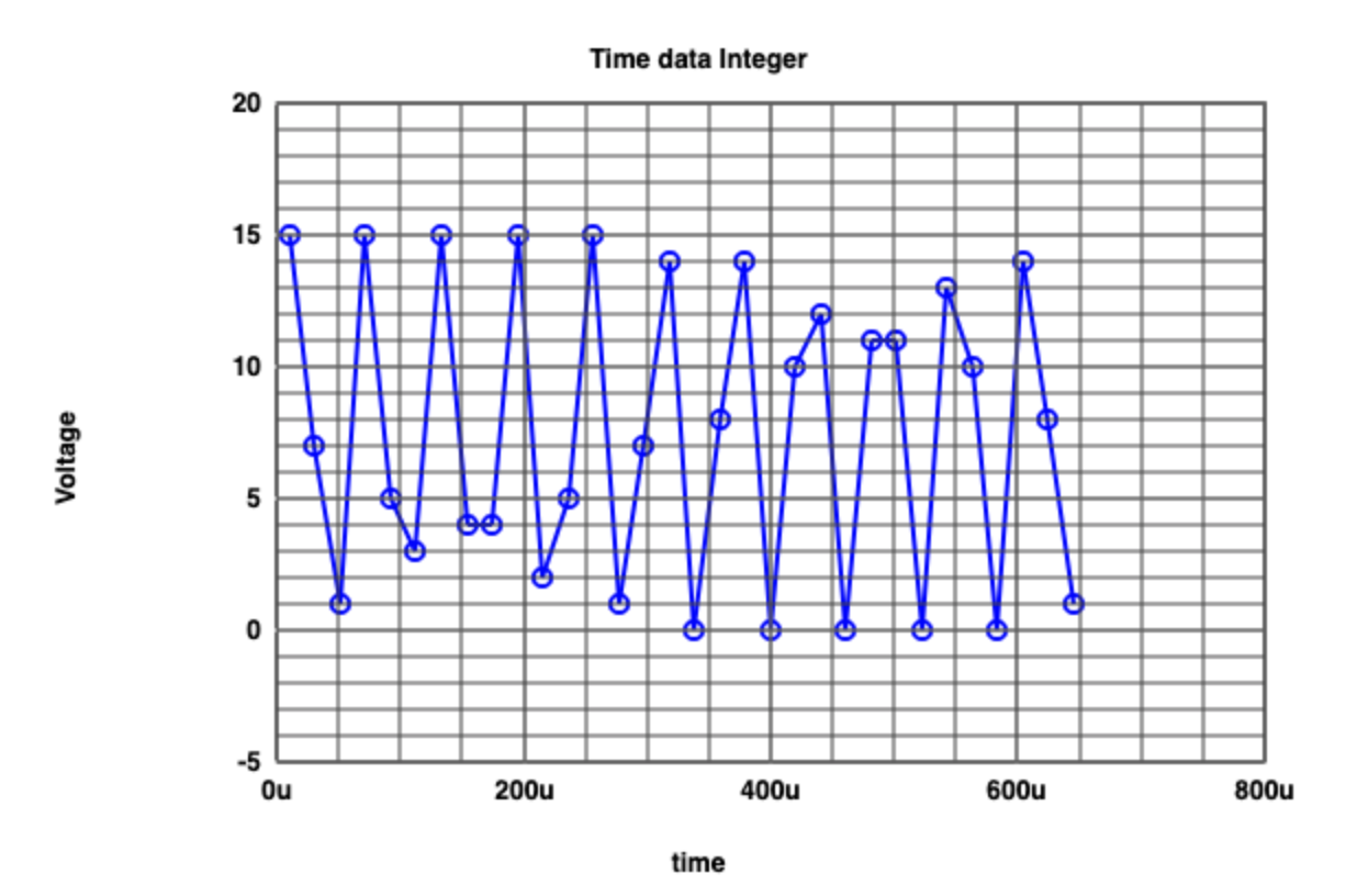
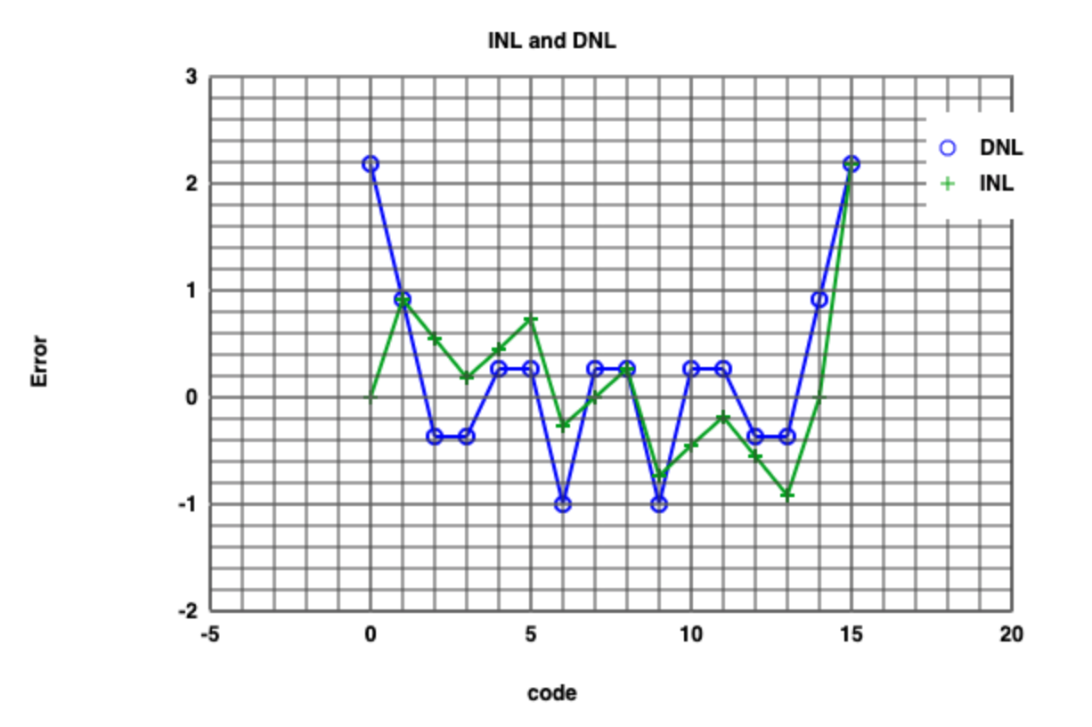
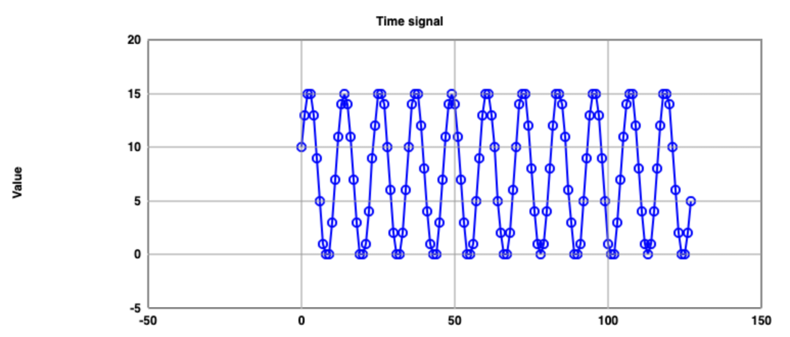
As previously mentioned, on the upper right side is the simulation result of Read Raw File from 4 bit ADC and DAC. However, here, the sampling rate is chosen as 5.12 µs (128 sampling points). Each step has 8 sampling points. Furthermore, it ideal curve is deviated due to offset error. Compared to previous slide, DNL and INL static errors can be obtained. |
  |
  |
Simulation Results of 4 bit ADC and DAC with Sine Input Signal by Simulator of Read Raw File
|
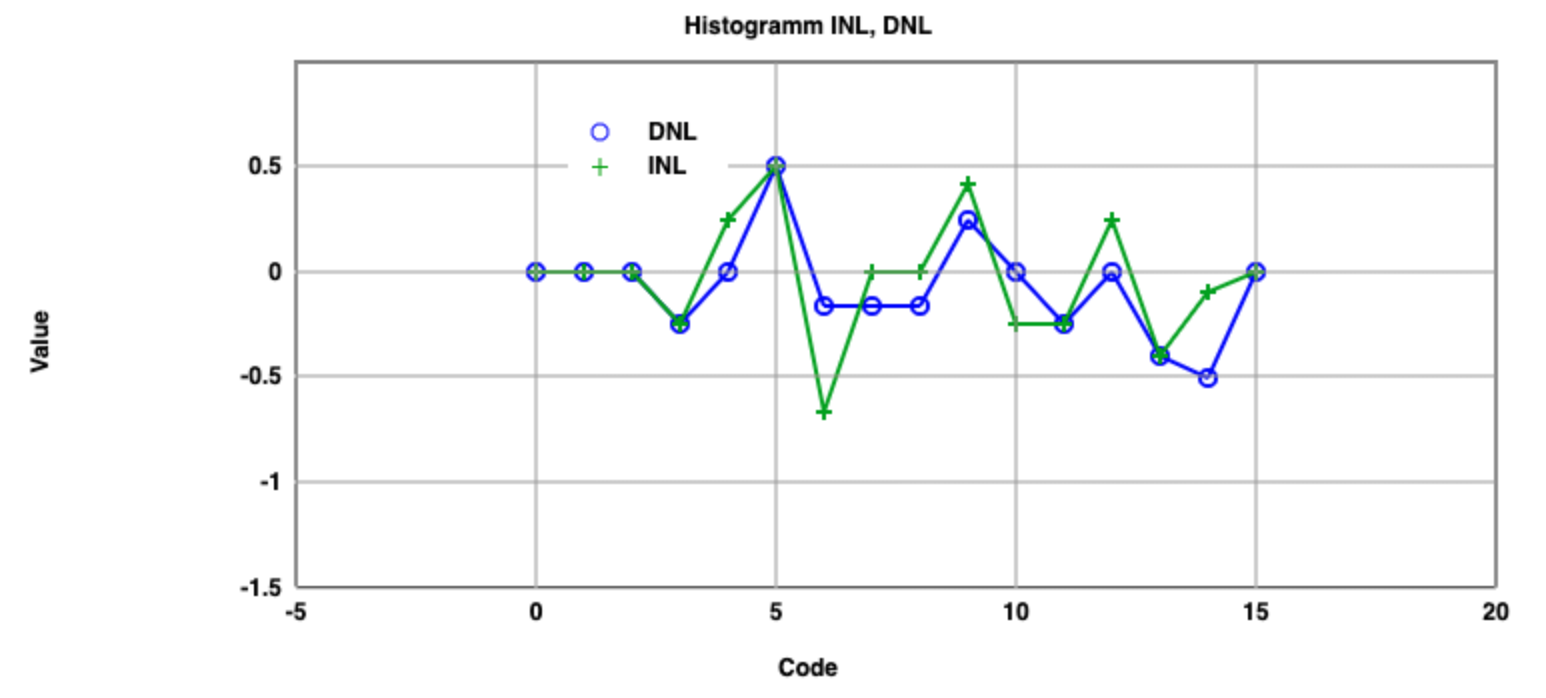
Extracted values of sine signal is sampled with time of 5.12 µs which corresponds to 128 points. On the right side, the extracted values of sine signal is sampled with time of 20.48 µswhich corresponds to 32 points. However, it is assumed that aliasing can occur. In the figure below, Sine histogram test is shown (DNL and INL errors). The typical bath tub shape of sine signal is also seen. |
  |
  |
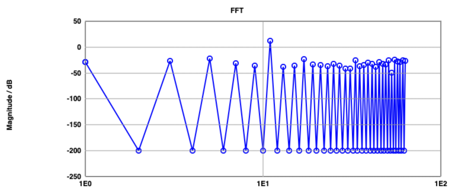
Simulation Results of 4 bit ADC and DAC by Simulator of FFT
|
On the right side, the simulation results of FFT of 4 bit ADC and DAC by using the webpage simulator. From the figure of FFT, frequency components are observable. The noise is also there. Moreover, the INL and DNL for sine signal is present. |
  |
 |
Signal to Noise Ratio form Simulation Results of 4 bit ADC and DAC by Simulator of FFT
- Table for Signal to Ratio
| Frequency | Signal magnitude (dB) | Total noise magnitude (dB) |
| 11 | 11.87 | -13.89 |
| 5 | -21.56 | -14.7 |
| 17 | -23.64 | -15.3 |
| 55 | -24.16 | -15.9 |
| 61 | -25 | -16.47 |
| 51 | -25.62 | -17.04 |
| 33 | -25.67 | -17.68 |
| 63 | -26.33 | -18.31 |
| 3 | -26.86 | -18.96 |
| 57 | -27.66 | -19.59 |
| 1 | -28.4 | -20.21 |
4 bit ADC and DAC with R2R
|
In this part, the old 4 bit ADC and DAC has now R2R which is a collection resistors, connected at the four digital outputs. This can influence the digitalized analog output signal and further errors. For the simulation, the R2 and R8 values are changed from 2k to 1.5k and 1k to 1.3krespectively. |
|
LTSpice Simulation Results of 4 bit ADC and DAC With R2R
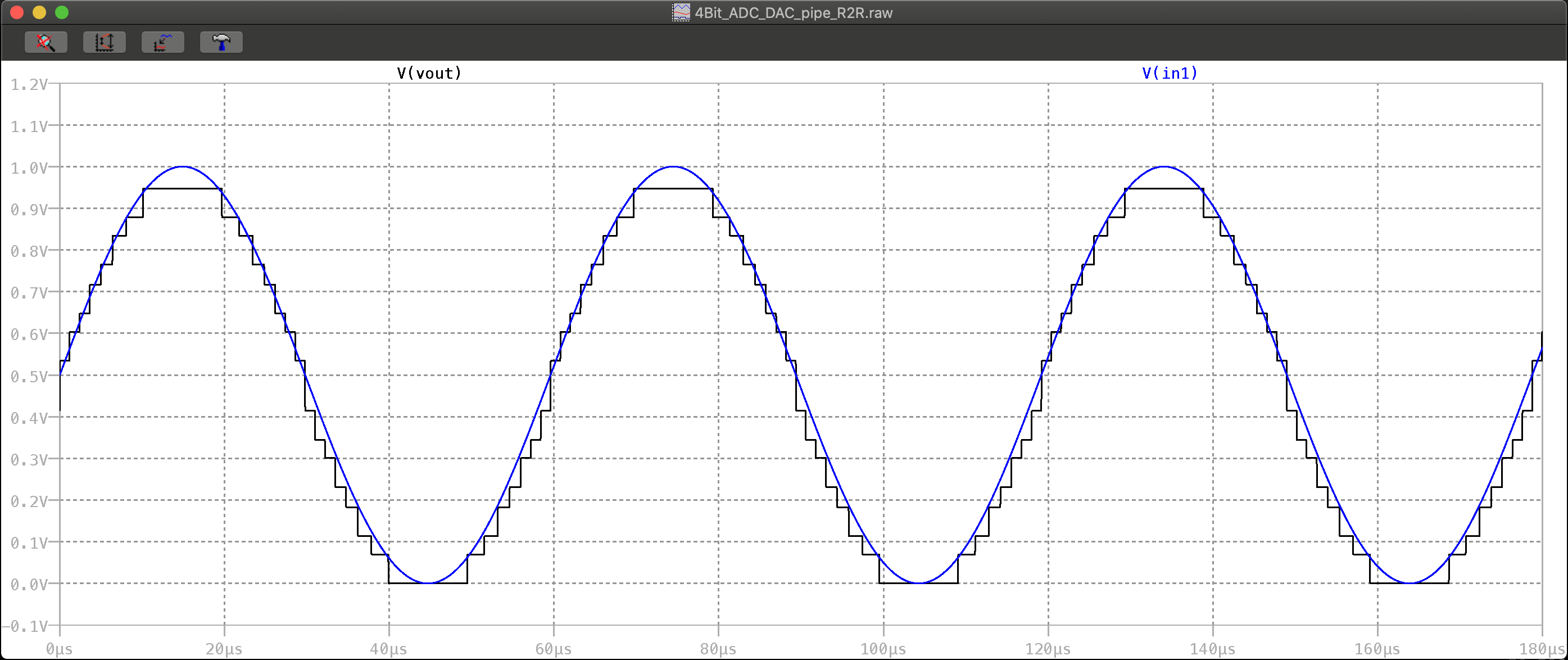
Ramp simulation result of 4 bit ADC and DAC with R2R which does not have fixed resistances. Compared to previuos ramp which
has constant LSBs this case, however, different steps (LSB) can be seen. This will lead to static error.
Even thoughh it has 15 steps, same is observed for the sine signal as well.
Simulation Results of 4 bit ADC and DAC with R2R by Simulator of Read Raw File (Ramp Signal)
|
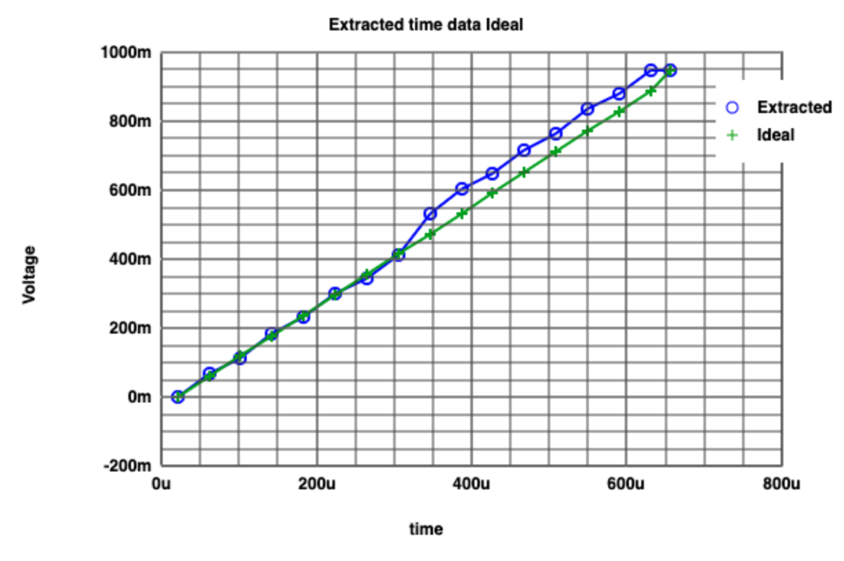
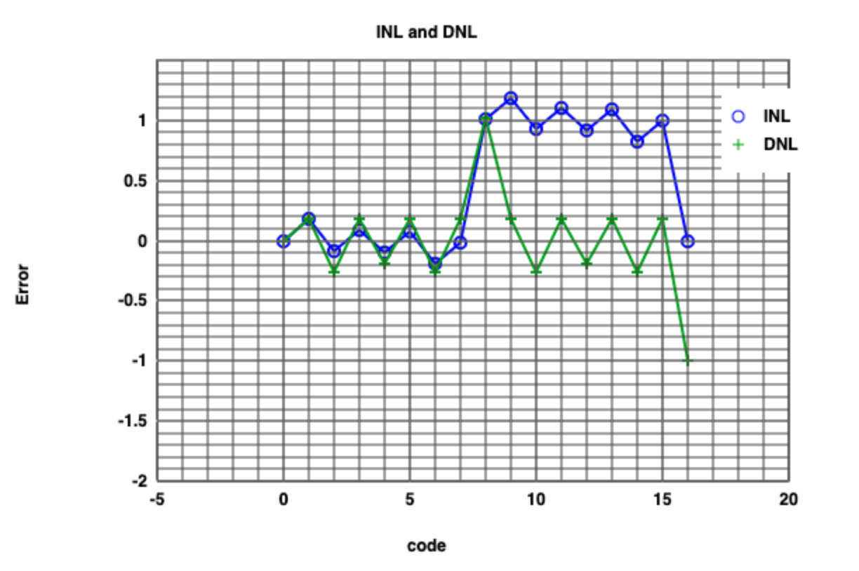
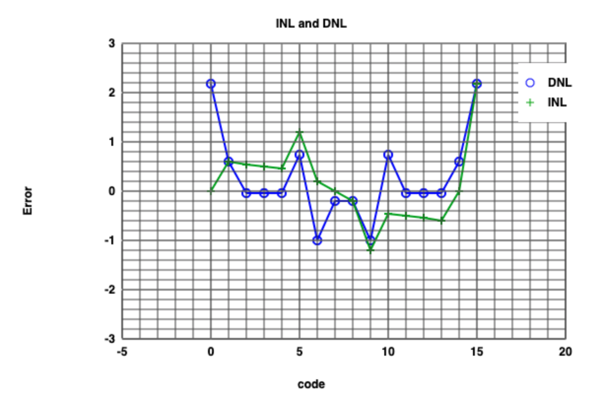
The extracted and ideal ramp signal is below has now noticeable deviation from the ideal ramp compared to simulation results from the converters without R2R. Especially, starting from 8th step. Similarly, the static errors such as INL and DNL are high when it comes to 8th steps. This indicates that R2R circuit connected to DAC causes static errors to happen. |
  |
Simulation Results of 4 bit ADC and DAC with R2R by Simulator of Read Raw File (Sine Signal)
However, due to uneven LSBs, deviations are still present. INL and DNL are changed its bathtub shape (it has deviated), especially code number 6,7, 10 and 11. |
  |