Interface ElectronicsLaboratory 01GroupA06, ***093, ZADC and DAC LTSPICE simulation |
Overview
- Installation webpage template
- Test for 4 Bit ADC and DAC
- Test for 3 Bit DAC
- Calculation of INL and DNL for the 3 Bit DAC
- Summary
- References
Installation of webpage
- Download the template.zip file
- Unzip the file
- Go to directory InEl_P2019
- Copied the directory 2019_GroupX to 2020_Group<xx>_Lastname
- In the directory copy the file: 2017_Group01_V00.html to 2020_Group<xx>_V1<Lastname>
- Edit with Notepad++ or other text editor: 2020_Group<xx>_V1<Lastname>
- Change the header, footer and made slide overview and installation
Test for 4 Bit ADC and DAC
|
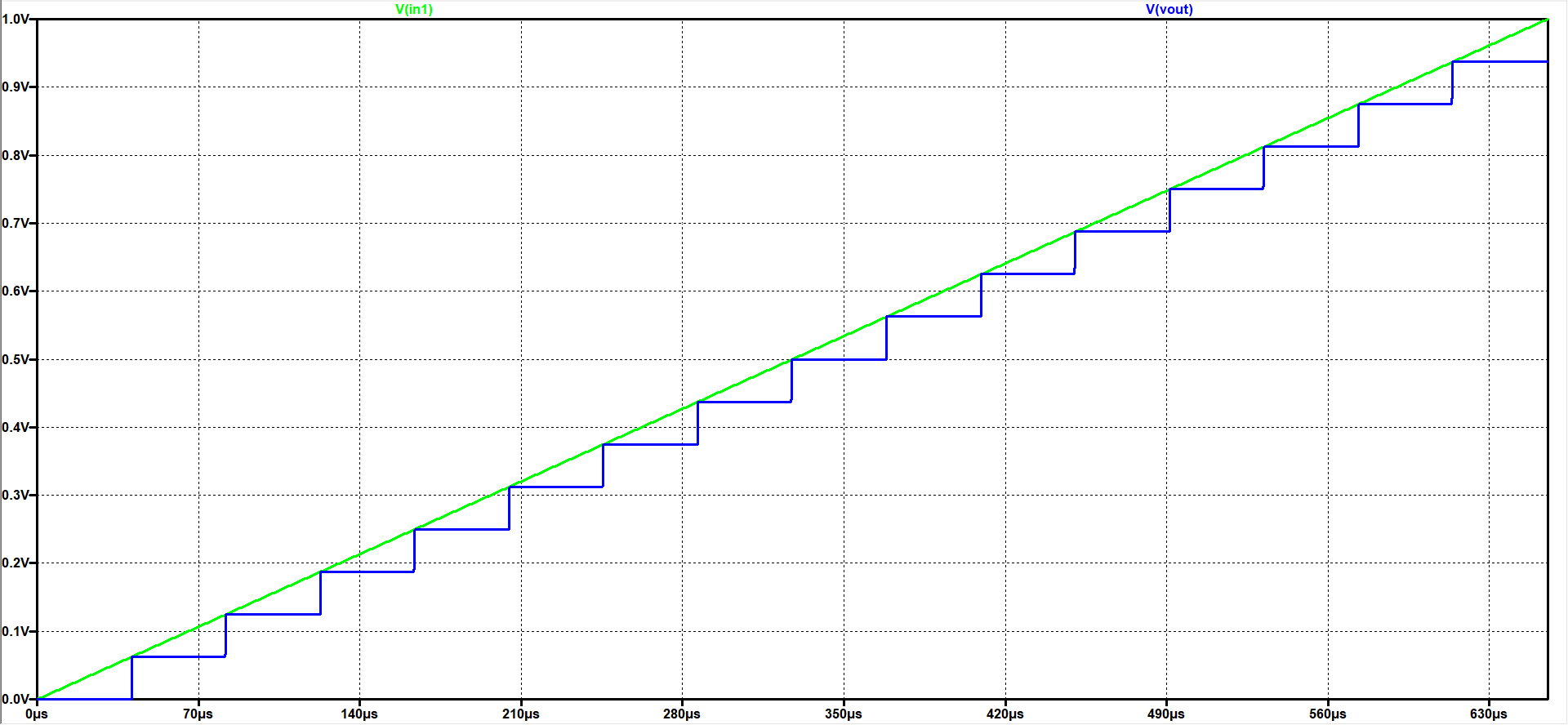
A 4 Bit ADC and DAC test can be simulated in LTSPICE. The files were downloaded and LTSPICE simulation was started. The output file size can be limited by using the .save dialog option. A voltage source was added with a ramp from 0V to 1V with a rise time time of 655µs. The picture shows a ramp inputvoltage and the DAC ramp output voltage over time. 16 steps can be seen. With a measurement statement the voltage levels were extracted. .measure tran V0000 find V(Vout) at=20u At 60µs time the output of 0.0625V is given for the code 0001. V0001: V(Vout)=0.0625 at 6e-005 No error in the voltage level can be seen. It is an ideal ADC and DAC.  |
Test for 3 Bit DAC
|
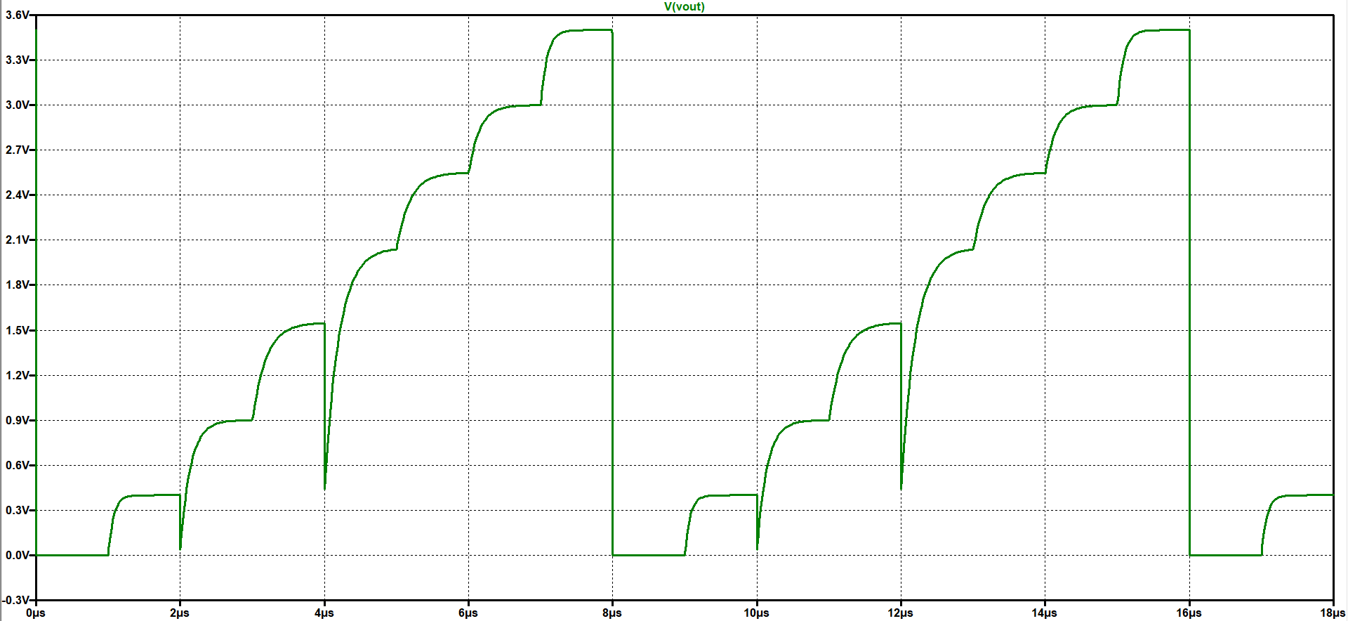
A 3 Bit DAC test can be simulated in LTSPICE. The file were downloaded and LTSPICE simulation was started. The picture shows the DAC ramp output voltage over time. 8 steps can be seen. With a measurement statement the voltage levels were extracted. .measure tran V0000 find V(Vout) at=0.95u At 1.95µs time the output of 0.399999V is given for the code 0001. V0001: V(Vout)=0.399999 at 1.95e-006 Some errors in the voltage level can be seen. So it can be said that it is a real DAC.  |
Calculation of INL and DNL for the 3 Bit DAC
Integral non linearity characterizes the difference between real and ideal transfer characteristics.Differential non linearity characterizes the step size (difference) between 2 successive codes.
|
Step size:
\( LSB = \frac{Vref }{2^{3}-1} = 0.5714V \) The difference between real and ideal output value is normalized with LSB and calculated as INL: \( INL(n) = \frac{ Vreal(n) - Videal(n)}{LSB} \) The step size between 2 successive codes is normalized with LSB and calculated as DNL: \( DNL(n) = \frac{ V(n) - V(n-1) - LSB}{LSB} \) Since the LSB is calculated using the first and last code: \( \sum DNL_i = 0 \) The graphs and the table represent the same data and contain the same information. |
Summary
- With Notepad++ it is possible to edit the HTML code of a website
- Simulation of an ideal ADC and DAC extended the understanding of this components
- Learned how to measure values in LTSpice by using a .meas file
- Due to different resistor values we obtain a real ouput characteristic and INL/DNL values
- By the calculation of INL/DNL the content of the lectures was strengthened
- Basic understanding of HTML code was learned