Interface ElectronicsLaboratory 01GroupB1, ****38, H |
Overview
- install webpage template
- Download LTspice files
- Simulation analysis
- Summary
installation of Webpage
- Download the template.zip.file
- Unzip the file
- Go to the directory InelP_2019
- Copied Directory 2019_GroupX to 2020_Group<XX>_<Lastname>
- in the directory copy the file : 2017_Group01_V00.html to 2020_Group<XX>_V1_<Lastname>
- Edit with notepad++ : 2020_Group<XX>_V1_<Lastname>
- changed the header, changed the footer , made slide overview, installation
Test for 4 Bit ADC and DAC
|
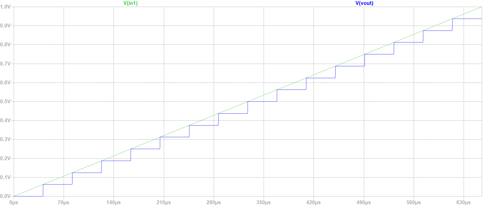
A 4 Bit ADC and DAC test can be simulated in LTSPICE. the file were downloaded and LTSPICE simulation was started. The output file size can be limited by using the .save dialog option. A voltage source was added with a ramp from 0to 1V with a rise time of 655µs. The picture shows a ramp input Voltage and the DAC ramp output voltage over 16 steps can be seen. with amesurments tatement the voltage levels were extracted .Measure TRAN V0000 FIND V(Vout) AT= 20u at 60ustimethe output of 0.0625 V is given for the code 0001. V0001: V(out)=0.0625 at 6e-005 No error in the voltage level can be seen. it is an ideal ADC and DAC. 
|
LTSPICE schematics
|
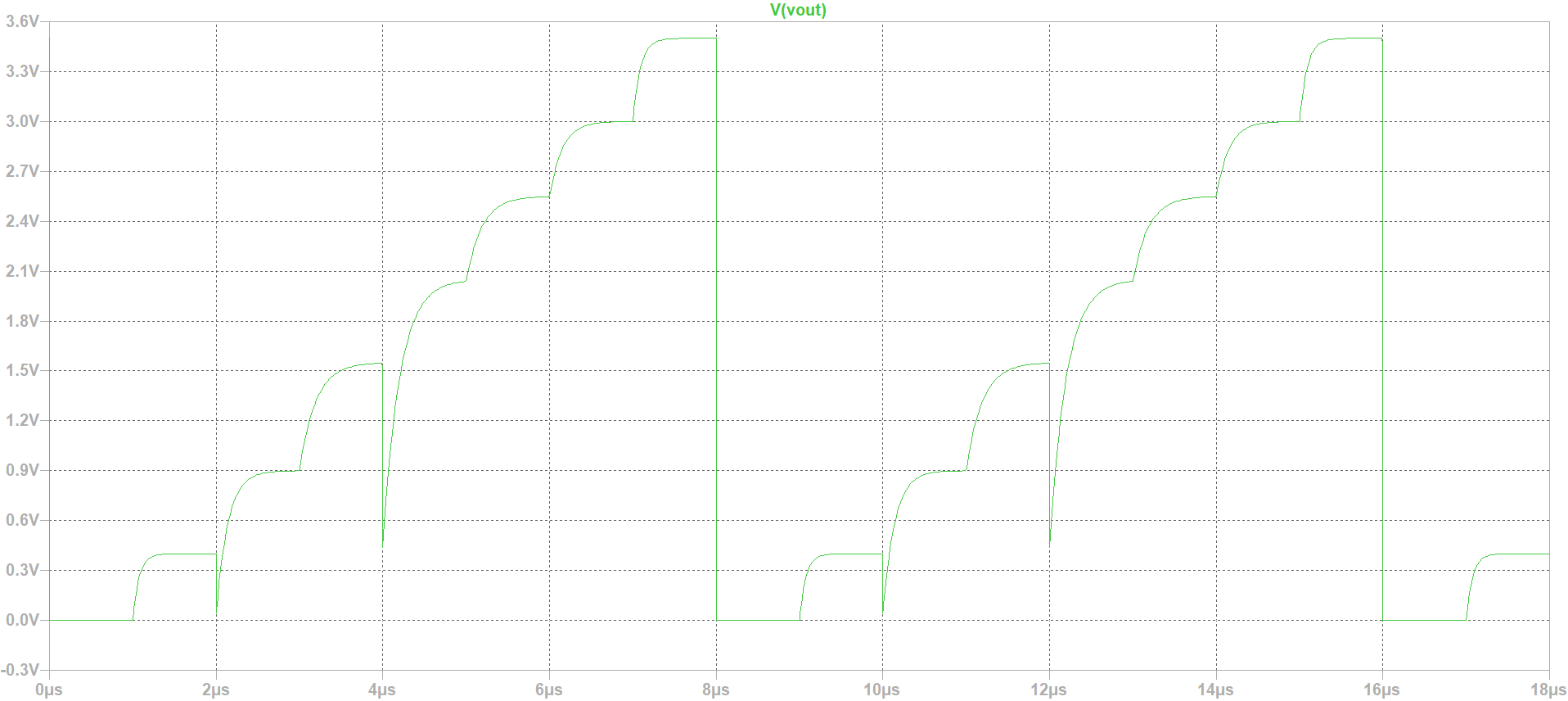
JavaScript module SPICE_HTML_2018_02/LTSPICE.js From the results it is clear that it is a real DAC, since we could see transition inthe voltage (due to transistor's C and R), also the different in R is responsible of inducing errors. Calculating DNL and INL: The first step is to calculate LSB=3.5/7=0.5v INL (011)= (Vreal-Videal)/LSB= -0.4v DNL= (Vn-Vn-1-LSB)/LSB=0.2v 
|
Summary
- This Lab allowed us to get more into HTML and Webpage creation, furthermore it allowed us to simulate different types of DAC. In case of real DAC we were wble to see errors and calculating INL and DNL.
Hochschule für angewandte Wissenschaften Kempten, Jörg Vollrath, Bahnhofstraße 61 · 87435 Kempten
Tel. 0831/25 23-0 · Fax 0831/25 23-104 · E-Mail: joerg.vollrath(at)fh-kempten.de
Impressum